Work Package 5 IC technologies - Leader: M.Campbell Deputy: F.Faccio - CERN Indico
←
→
Page content transcription
If your browser does not render page correctly, please read the page content below
Work Package 5
IC technologies
   Leader: M.Campbell
    Deputy: F.Faccio
Overview of Work Package 5

Ac#vity 1                                             Ac#vity 2
CMOS and assembly Technologies                        Design and IPs

1. CMOS Technologies                                  1. Low-voltage and low-power design
Leader: K.Kloukinas                                   Leader: R. Ballabriga Sune

Radia%on effects                                       Build-up and share experience in ASIC design
 CAD tools with emphasis on:                          Design/characterisa%on of building blocks:
 - reference design workflows                          - Voltage reference generators
 - mixed-signal design of complex chips (SOC)         - Low-noise amplifiers
 - collabora%ve tools                                 - Conversion: ADC, DAC
Enablers (DKit, FrameContract, NDA, training)         - Timing circuits: PLLs, DLLs, TDC
Custom digital logic compilers                        - Line drivers/receivers

                                                       2. Power distribu#on
                                                      Leader: S.Michelis
CMOS-related Assembly Technologies
                                                      High efficiency DCDC converter (Vin >25V)
 Through-Silicon Vias (TSV)                           IP blocks for on-chip power management:
 CMOS wafer stacking                                     converters and regulators
Recent history of CMOS processes used in HEP
#me
2025 28nm CMOS?
22nm FDSOI?
14nm FinFET?
2020
2014
65nm
12 designs (HL-LHC)
2009 130nm
26 designs (HL-LHC)
1998 0.25um
>50 designs (LHC)
End Of Life 2019
size, complexity, radia#on specsActivity 1
CMOS Technologies Environment
Radia#on hardness design prac#ces
Accessibility
Frame contract, NDAs, framework
Selec%on Criteria
for collabora%ve design
Radia#on tolerance CAD Enablers
Easy access Mixed-Signal Design Kit, Reference
Design Workflow
Support from manufacturer
MVP
Long-term availability Elementary macro-blocks
Cost IO pads, ESD structures,
….. Digital Logic Compilers
Training and knowledge build-up
Specialised courses, Blogs and Web
interfaces, Sharing of experience
IP blocks (WP2.1)
Complex macro-blocks characterised
on silicon and ready for use
* I adopt here the defini%on of “MVP” for a technology introduced by M.Garcia Sciveres (LBL) in a presenta%on
about the development of the FEI4 chip for the ATLAS pixel detectorWork-plan for Activity 1 and 2.1
2020 2021 2022 2023 2024 2025
Radia%on tests
Global evalua%on
MVP Commercial/legal framework
Ac#vity 1
Elementary macro blocks
CMOS Technologies
CAD environment
Training
Design & prototype
Ac#vity 2
Qualifica%on
Design and IP blocks
2.1 Low-voltage and low-power design Move to produc%onActivity 2.2: Power distribution
High efficiency DCDC converter (Vin >25V)
Existing today
bPOL2V5/rPOL2V5
optoelectronics
FEAST2/bPOL12V
1.2V
Stage2 analog
48V 12V 2.5V
Stage 0 Stage1 0.8V
Stage2 digital
LinPOL
1.5-3.3V
Linear slow control
>25V 2.5V
Stage 1
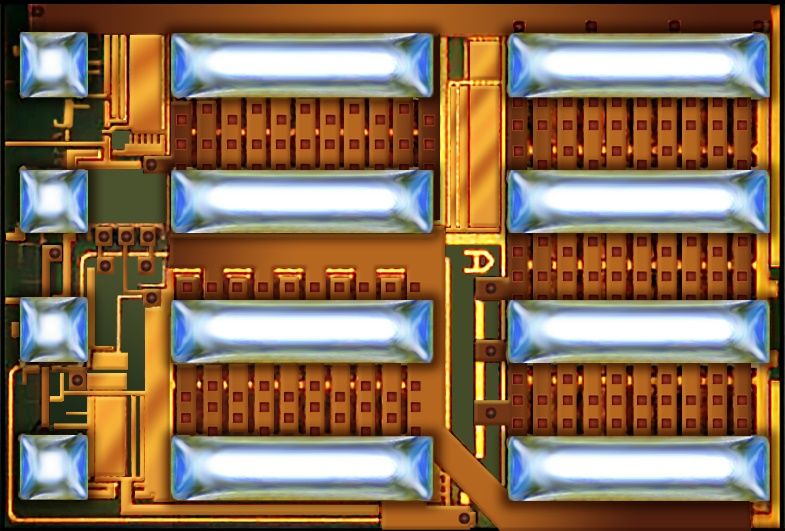
6One very ahrac%ve possibility: Switched Tank Converter (STC) using GaN power transistors
Divide-by-4 STC from 48V input, 50-100W power, efficiency >98%
In HS
In HS
In HS
In LS
In LS
In LS
Control
+boots
ASIC
+boots
+boots
Logic
Logic
Logic
trap
trap
trap
EPC2151 – 80 V, 10 A Integrated DrGaN Half-Bridge
shifter
shifter
shifter
Power Stage - PRELIMINARY
Level
Level
Level
Functional Block Diagram
driver
driver
driver
driver
driver
driver
Vin=48V Vout=12V
driver
driver
driver
driver
driver
driver
New fully GaN product with power
shifter
shifter
shifter
Level
Level
Level
transistors,
Die Photo drivers and level shijer
+boots
+boots
+boots
Logic
Logic
Logic
trap
trap
trap
In HS
In HS
In HS
In LS
In LS
In LS
3.9 mm x 2.6 mm x 0.8 mm
GaN power devices can be used also in other topologies, where they open the path for high-efficiency and
large conversion ra%o buck converters (25V->2.5V, for instance)
Subject to Change without Notice www.epc-co.com COPYRIGHT 2019 Page 6Work-plan for Activity 2.2
2020 2021 2022 2023 2024 2025
Radia%on test of
Ac#vity 2 GaN component
Design and IP blocks
Prototype DCDC
2.2 Power distribu%on
with simple control
Prototype DCDC with
integrated control (ASIC)
Design and qualifica%on
Radia%on test of silicon (CMOS)
of complete prototype(s)
High-V technologies Review
Prototype DCDC with
integrated control (ASIC)Present structure of Work Package 5
Ac#vity 1 Ac#vity 2
CMOS Technologies Design and IPs
1. CMOS Technologies 1. Low-voltage and low-power design
Leader: K.Kloukinas Leader: R. Ballabriga Sune
Radia%on effects Build-up and share experience in ASIC design
CAD tools with emphasis on: Design/characterisa%on of building blocks:
- reference design workflows - Voltage reference generators
- mixed-signal design of complex chips (SOC) - Low-noise amplifiers
- collabora%ve tools - Conversion: ADC, DAC
Enablers (DKit, FrameContract, NDA, training) - Timing circuits: PLLs, DLLs, TDC
Custom digital logic compilers - Line drivers/receivers
2. Power distribu#on
Leader: S.Michelis
High efficiency DCDC converter (Vin >25V)You can also read