ARCADIA INFN CSNV Call Project - IDEA Collaboration Meeting Bologna, June 14th 2019
←
→
Page content transcription
If your browser does not render page correctly, please read the page content below
ARCADIA INFN CSNV Call Project
              IDEA Collaboration Meeting
                 Bologna, June 14th 2019
                             Manuel Da Rocha Rolo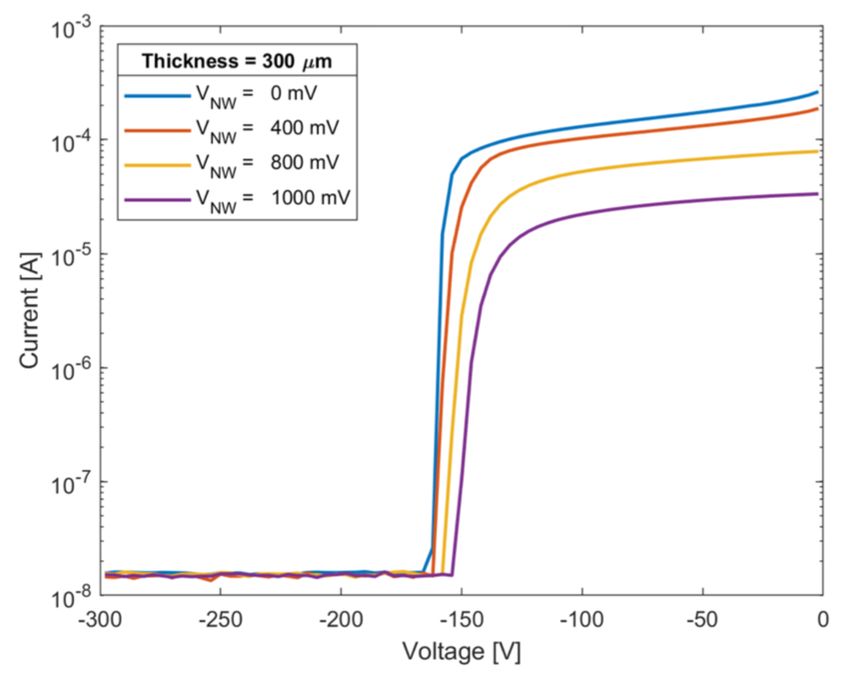
Fully depleted CMOS MAPS at INFN
     Ongoing activity towards a CMOS sensor design and fabrication platform allowing for:

      ✴ Active sensor thickness in the range 50 μm to 500 μm or more;

      ✴ Operation in full depletion with fast charge collection only by drift;

      ✴ Small charge collecting electrode for optimal signal-to-noise ratio;

      ✴ Scalable readout architecture with ultra-low power capability (O(10 mW/cm2));

      ✴ Compatibility with standard CMOS fabrication processes: concept study with
        small-scale test structure (SEED), technology demonstration with large area
        sensors (ARCADIA)

      ✴ Use of a deep sub-micron 110nm CMOS node for higher gate density
!2   Status of the ARCADIA INFN CSNV Call Project                                     Bologna, 2019-06-14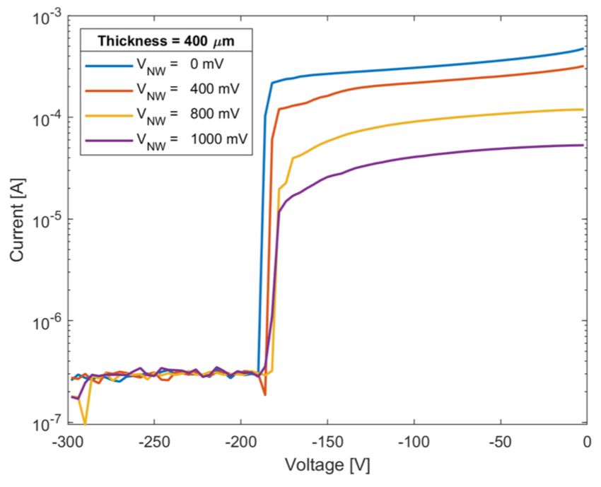
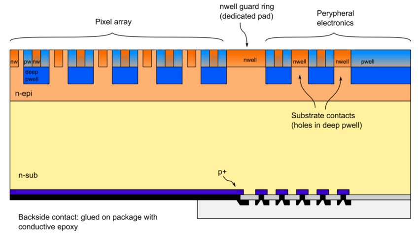
Fully depleted CMOS: the sensor

                                                                                                                              SEED
                                                                                                                              Sensor with

                                                                                                                              Embedded

                                                                                                                              Electronics

                                                                                                                              Development

               • Technology: 110 nm CMOS CIS technology, high-resistivity bulk

               • Custom backside process developed in collaboration with LFoundry*

               • Both NMOS and PMOS transistors

               • Patterned backside, the main diode is surrounded by a guard-ring
                                                    * LFoundry and SMIC have entered into a binding agreement for which 100% of the shares of LFoundry are
                                                      sold to Jiangsu CAS-IGBT Technology Co., Ltd. The formal acquisition is scheduled for the end of June

!3   Status of the ARCADIA INFN CSNV Call Project                                                                                           Bologna, 2019-06-14
Small-scale CMOS MAPS demonstrator

100 V

120 V

140 V

     Map of pixel reset voltage (MATISSE 24x24 pixel matrix, 50um pixel, CDS readout) as a function
     of the back-side voltage applied to the sensor. Depletion starts from the back-side.
!4      Status of the ARCADIA INFN CSNV Call Project                                        Bologna, 2019-06-14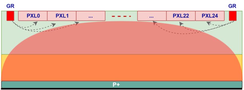
Depletion studies (100-400 µm thickness)

                                                             IV-curve of a 400x400 µm2
                                                             pseudo-matrix test chip (8x8
                                                             50x50µm2 pixels)

                                                             Full depletion studies in
                                                             100-300-400 μm prototypes

     100 µm                                         300 µm           400 µm

!5   Status of the ARCADIA INFN CSNV Call Project                                           Bologna, 2019-06-14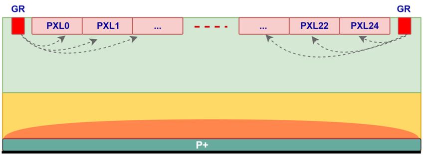
ARCADIA (INFN CSNV Call Project)
     Advanced Readout CMOS Architectures with Depleted Integrated sensor Arrays

       ✦ target pixel size below 25 μm x 25 μm

       ✦ binary readout, ToA VCO on chip periphery (p/ double column)

       ✦ embedded electronics performing sparsified readout

       ✦ matrix of 512 x 512 cells, architecture scalable to 2048 x 2048

       ✦ modular architecture for a straightforward scaling of the design to a reticle-size sensor

       ✦ DRC compliant with 2D stitching assembly, towards wafer-scale silicon

                                      Dedicated mask set: reticle size 2.6 cm x 3.2 cm
                                      Engineering run by mid-2020

!6    Status of the ARCADIA INFN CSNV Call Project                                          Bologna, 2019-06-14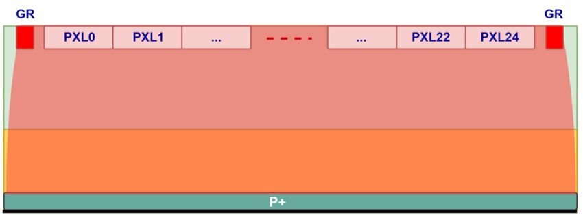
ARCADIA - Demonstrator Chip

       data-driven readout and low-power asynchronous architecture for data and control signal transmission
     ✦ Low-power clockless matrix and zero-suppressed readout, event rate power driven; Hit OR fast
           propagation from pixel to End-of-Column, OR
     ✦ Low-frequency clock propagated through matrix, on-pixel time interpolation (possibly also ToT)
       Counting mode implemented in periphery
       Very low-power mode with “strip-like” functional configuration of the full column

!7   Status of the ARCADIA INFN CSNV Call Project                                                  Bologna, 2019-06-14
Project status and ongoing activities
01/2019 01/2022
TCAD 2D/3D sensor simulation: geometry, p-well spacing, node capacitance, transient
CMOS Analogue IP block design: bandgap, continuous and discrete-time very-front-
ends, prototyping run October 2019
CMOS Digital IP block design:
post-synthesis simulations at pixel and column level (128-pixel region), without SDF
good progress on CAD/EDA tools integration for LF11is iPDK
tentative pixel floorplan placement: below 100um2, constraint-less
Data acquisition: planned short-term development for a “pocket” DAQ for MATISSE
Characterisation: laser and microbeam tests with pseudo-matrices @RBI, Zagreg
!8 Status of the ARCADIA INFN CSNV Call Project Bologna, 2019-06-14Outlook
01/2019 01/2022
ARCADIA will build a design, characterisation and production framework for fully-
depleted MAPS in a CMOS commercial foundry
Future collaborations, funding and resources will allow for the development of
application-specific wafer-scale sensors for frontier detectors, medical, space and
industrial applications
Expressions of interest and opportunities: design of 2D-stitched wafer-scale
demonstrators, scalable DAQs, mechanics and cooling for large systems, ultra-thinned
silicon handling and assembling, integration of system-grade design, space qualification
!9 Status of the ARCADIA INFN CSNV Call Project Bologna, 2019-06-14ARCADIA Advanced Readout CMOS Architectures with Depleted Integrated sensor Arrays INFN - Bologna, Milano, Padova, Perugia, Pavia, TIFPA, Torino A. Gabrielli, D. Falchieri, G. D’Amen, F. Alfonsi, N. Giangiacomi, A. Cervelli, A. Andreazza, M. Caccia, R. Santoro, A. De Angelis, P. Giubilato, J. Wyss, A. Candelori, R. Rando, D. Bastieri, G. Ambrosi, P. Placidi, D. Passeri, T. Croci, L. Servoli, A. Scorzoni, G. Traversi, L. Ratti, , M. Pezzoli, C. Vacchi, L. Gaioni, L. Pancheri, G.-F. Dalla Betta, A. Ficorella, M. Zarghami, M. Favaro, R. Iuppa, S. B. Ricciarini, P. Zuccon, F. Nozzoli, B. Di Ruzza, E. Ricci, M. Da Rocha Rolo, R. Giampaolo, A. Rivetti, S. Beolè, R. Wheadon, F. Tosello, N. Demaria, A. Di Salvo, G. Dellacasa, J. Olave, M. Mandurrino, A. Paternò Manuel Da Rocha Rolo, INFN TORINO Workshop on the Circular Electron-Positron Collider, 15 - 17 April 2019, Oxford, UK
You can also read