URANIA LNF MEETING - 5 Feb 2021 Pads number Readout Example of front-end stages Conclusions & to do list
←
→
Page content transcription
If your browser does not render page correctly, please read the page content below
URANIA LNF MEETING – 5 Feb 2021
• Pads number
• Readout
• Example of front-end stages
• Conclusions & to do list
8 CHANNELS ARE BETTER THAN 9 …

 CONSTRAINTS
 • Gain ≃ 500
 • Primary electrons ≃ 20.000 electrons
 • Charge ≃ 1.6 pC à 0,5 pC (gas gain fluctuation/geometry)
 • Pad Capacitance(3x3 cm^2) ≃ 240 pF (er kapton =3)
 • N. Channels: 9
 • Analog outputs for external waveform digitizing

CONSTRAINTS
• Gain ≃ 500
• Primary electrons ≃ 20.000 electrons
• Charge ≃ 1.6 pC à 0,5 pC
• Pad Capacitance(2.5x5 cm^2) ≃ 330 pF (er kapton =3)
• N. Channels: 8
• Analog outputs for external waveform digitizing

G. Felici                               URANIA - 5 Feb 2021   2
READOUT ASSEMBLING EXAMPLE
Only 8 channels --> discrete readout can be used
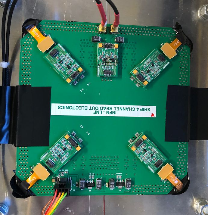
• Mother Board
• Front-End Daughter Boards (4 or 8 channels)
• More expensive but more flexible FRONT-END
DAUGHTER BOARD
INTERCONNECTION READOUT MB ACTIVE AREA
ANALOG OUTPUT
(MCX)
FRONT END
DAUGHTHER BOARDS FARADAY CAGE DETECTOR PCB
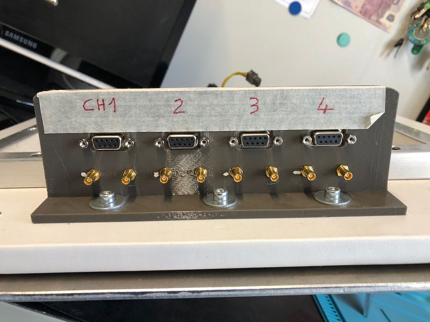
EXAMPLE: FC INTERCONNECTION PANEL
EXAMPLE: 15x15 cm2
scintillator tile readout
SERVICE CONNECTORS
MOTHER BOARD SIGNAL CONNECTORS
SCINTILLATOR TILE (BELOW)
MOTHER BOARD CAN HOST
HV CONNECTIONS
G. Felici URANIA - 5 Feb 2021 3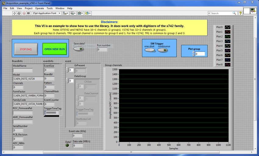
DIGITIZING DETECTOR SIGNAL IS BETTER TO UNDESTAND DETECTOR BEHAVIOUR
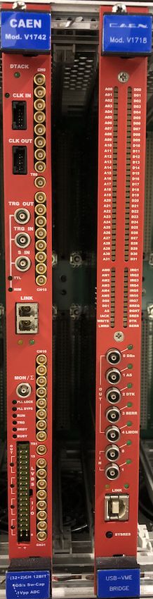
EXAMPLE: DIGITIZING CHAIN USED FOR BTF SHADOW TEST BEAM (ALESSANDRO CALCATERRA)
CAEN FADC
• V1742
CAEN
• 32 + 2 chs
Crate
• 12 bits
Controller
• DRS4 BASED (1024 cells) LABVIEW DAQ
• 750MS/s - 5GS/s
+
ROOT MACRO
Self-trigger, combinations of channels over-
threshold in logic OR; common to couples of groups
TO BE INVESTIGATED
G. Felici URANIA - 5 Feb 2021 4READOUT: example 1 (no noise simulation - ideal component)
PREAMPLIFIER SHAPER AMPLIFIER COMPARATOR
SINGLE PAD
100 fC
SHAPING DO NOT MATCH THE V1742 TIME WINDOW SPAN
G. Felici URANIA - 5 Feb 2021 5Gain and input impedance. As can be seen from the small signal model, the equivalent input
impedance of the preamplifier
READOUT: is equal
Solving (2.1)to:
examplefor vo2(having
(no noise calculation
disabled - ideal component)
in1 ) one obtains:
1
rin = 1/gm1 . vo (s) = ii RL , (2.2) (2.3)
(1 + st)
The input impedance ofwhere t = Cd rindepends
the amplifier . As onedirectly
can see,on thethe transconductance
response ofpole.
has only one the transistor
In order M .
to 1obtain a response
equivalent to a CR (RC) n , the shaper is implemented as n stages of low pass filter with the time
By stabilizing the current in the transistor, one can obtain constant impedance, which is suitable as
constant t. Its
a termination of the transmission transfer function is given by:
line.
1
H(s) = . (2.4)
(1 + st)n
SINGLE PAD
Consequently, the vo f can be written as:
–5–
1
vo f (s) = ii RL . (2.5)
(1 + st)n+1
The circuit response in the time domain to the delta current pulse (1.1) can be calculated as:
Qi RL 1 ⇣ t ⌘n t
100 fC
vo f (t) = e t.
100 fC(2.6)
t G(n + 1) t
The maximum amplitude of the response is given by:
HIGHER BANDWIDTH (AND HIGHER Qi RL NOISE)
1 ⇣ n ⌘n
vo f max = . (2.7)
t G(n + 1) e
t1=t2=tm
The signal gain of a common gate amplifier directly depends on the load resistor RL and the pa-
(formatura triangolare)
rameters of the filter following the preamp.
Noise contribution from M1 . To calculate the equivalent input noise contributed by M1 we as-
sume that the noise generator in1 is turned on while the ii is off. Consequently, by solving (2.1) and
G. Felici URANIA - 5 Feb 2021 6
(2.4), we can write:
stCONCLUSIONS
• 8 pads (2.5 x 5 cm^2)
• Compact readout (no interconnection wires used in sensitive area)
• Mother Board and Daughter Board readout assembling (different FE stages can be easily tested)
• If using V1742 digitized the maximum acquisition time window is about 1.6 us
• A faraday cage should be used to minimize external pickup
NEXT STEPS
• Design/Simulation/Test/Optimization preamp configuration
• Mother board - detector assembling system ASSUMING FC
• HV connections
DEADLINES ???????
G. Felici URANIA - 5 Feb 2021 7You can also read