PFH500 Series Instruction Manual - TDK Product Center
←
→
Page content transcription
If your browser does not render page correctly, please read the page content below
TDK-Lambda
PFH500-SERIES
INSTRUCTION MANUAL
PFH500 Series
Instruction Manual
BEFORE USING THE POWER SUPPLY UNIT
Be sure to read and understand this instruction manual thoroughly before using this product. Pay attention to all cautions and
warnings before using this product. Incorrect usage could lead to an electrical shock, damage to the unit or a fire hazard.
DANGER
Never use this product in locations where flammable gas or ignitable substances are present. There are potential risks of igniting
these substances caused by arcing.
WARNING
Do not touch this product or its internal components while circuit is live, or shortly after shut down. There may be high voltage or
high temperature present and you may receive an electric shock or burn.
While this product is operating, keep your hands and face away from it as you may be injured by an unexpected situation.
Do not make unauthorized changes to this product, otherwise you may receive an electric shock. It will also void the product
warranty.
Do not drop or insert anything into the product. It might lead to a failure, fire or electric shock.
Do not use this product if abnormal conditions such as emission of smoke and/or abnormal smell, etc… are present. It might lead
to fire and/or electric shock. In such cases, please contact TDK-Lambda. Do not attempt to repair by yourself, as it is dangerous
for the user.
Do not operate these products in the presence of condensation. It might lead to fire or electric shock.
CAUTION
This power supply is designed and manufactured for use within an end product such that it is accessible only to trained SERVICE
ENGINEERS.
Confirm that the connections to input/output terminals, and signal terminals are correct as specified in this instruction manual
before turning on the power.
Input voltage, Output current, Output power, ambient temperature, case temperature, and ambient humidity should be kept within
the specifications, otherwise the product may be damaged.
Do not operate or store this product in an environment where condensation can occur. Waterproof treatment or special storage
and handling is necessary.
The equipment has been evaluated for use in a Pollution Degree 2 environment.
Do not use this product in environment with a strong electromagnetic field, corrosive gas or conductive substances.
For applications, which require very high reliability, such as nuclear related equipment, medical equipment, traffic control
equipment, etc., it is necessary to provide a fail-safe mechanism in the end equipment.
Do not inject abnormal voltages into the output terminals or signal terminals of this product. The injection of reverse voltage or
over voltage exceeding nominal output voltage into these terminals can damage the internal components of the product.
Never operate the product under over-current or short circuit conditions. Failure or other damage may occur.
The output voltage of this power supply unit is considered to be a hazardous energy level (The voltage is 2 V or more and the
electric power is 240 W or more). It must not be made accessible to users. Protection must be provided for Service Engineers
against indirect contact with the output terminals and/or to prevent tools being dropped across them. While working on this product,
the AC input power must be switched off, and the input, output, +VBus, and -VBus terminal voltages should be at a safe level.
The application circuits and their parameters are for reference only. Be sure to verify effectiveness of these circuits and their
parameters before finalizing the circuit design.
Use a Fast-Blow external fuse to each module to ensure safe operation and compliance with the safety standards to which it is
approved. The recommended input fuse rating within the instructions is as follows: 10A, 250V fast acting fuse. The breaking
capacity and voltage rating of this fuse may be subject to the end use application.
REV 3.0 (January 6, 2021) 1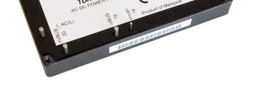
TDK-Lambda
PFH500-SERIES
INSTRUCTION MANUAL
CAUTION
This information in this document is subject to change without prior notice. Please refer to the latest version of the data sheet,
etc., for the most up-to date specifications of the product.
No part of this document may be copied or reproduced in any form without prior written consent TDK-Lambda.
REV 3.0 (January 6, 2021) 2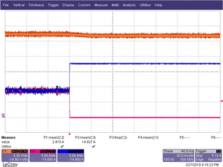
TDK-Lambda
PFH500-SERIES
INSTRUCTION MANUAL
Contents
BEFORE USING THE POWER SUPPLY UNIT ................................................................................................. 1
1 Model Name Identification Scheme.............................................................................................................. 5
1.1 Ordering Table 5
2 Module Pinout (Pin Side-Up)........................................................................................................................ 6
3 Circuit Block Diagram .................................................................................................................................. 7
4 Sequence Timing Diagram .......................................................................................................................... 8
5 Terminal Connecting Method ....................................................................................................................... 9
5.1 F1 External Input Fuse 10
5.2 C1 (1 µF); C4 (1 µF); C5 (2.2 µF) Film Capacitor or Class X Safety Capacitor 10
5.3 L1 (6.3 mH); L2 (6.3 mH) Common Mode Choke 11
5.4 C2 (3300 pF); C3 (3300 pF) Ceramic Capacitor or Class Y Capacitor 11
5.5 R1 (470 k, 2 W); R3 (470 k, 2 W); R4 (470 k, 2 W) 11
5.6 C6 (470 pF); C7 (470 pF) Ceramic Capacitor or Class Y Capacitor 11
5.7 Electrolytic Bulk Capacitors: C9 (470 µF); C10 (470 µF) 11
5.8 C11 (470 pF); C12 (470 pF) 12
5.9 C13 (0.1 µF, 50 V~100 V Ceramic Capacitor) 12
5.10 C14 (40µF, 50 V~100 V or (4) 10 µF Ceramic capacitors in parallel) 12
5.11 C15; C16 – Output Electrolytic Capacitors 13
5.12 R2 14
5.13 RL Inrush Relay (12 V Coil, 10 A / 277 Vac; 16 A / 125 Vac) 15
6 Explanation of Functions and Precautions ................................................................................................. 15
6.1 Input Voltage Range 15
6.2 Output Voltage Adjustment Range 15
6.3 Inrush Current 18
6.4 Output Over Voltage Protection (OVP) 18
6.5 Boost (or VBUS) Over Voltage and Under Voltage Protection (BOVP/BUVP) 18
6.6 Over Current Protection (OCP) 18
6.7 Over Temperature Protection (OTP) 19
6.8 Remote Sensing 19
6.9 ON-OFF Control 20
6.10 Power Good Signal (PGood) 20
6.11 Auxiliary Bias Power 21
6.12 OPTIONAL Droop Load Share (Parallel Operation) 21
REV 3.0 (January 6, 2021) 3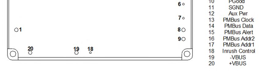
TDK-Lambda
                                                                                                                                      PFH500-SERIES
                                                                                                                                INSTRUCTION MANUAL

      6.13 PMBus Communication                                                                                                                                 22
      6.14 Ripple and Noise                                                                                                                                    23
      6.15 Series Operation                                                                                                                                    24
      6.16 Isolation Resistance                                                                                                                                25
      6.17 Withstand Voltage Test (Hipot Test)                                                                                                                 25
 7    Thermal Considerations and Mounting Method .......................................................................................... 27
      7.1     Thermal Consideration                                                                                                                            27
      7.2     Output Current / Case Temperature Thermal Derating                                                                                               28
      7.3     Recommended Soldering Condition                                                                                                                  29
      7.4     Recommended Washing Condition                                                                                                                    29
 8    Troubleshooting Guide............................................................................................................................... 30
 9    Warranty Period ......................................................................................................................................... 31
 10 Appendix.................................................................................................................................................... 32
      10.1 EMI Conducted Emissions CISPR 32:2015 Class B Recommended Values                                                                                    32

REV 3.0 (January 6, 2021)                                                                                                                                             4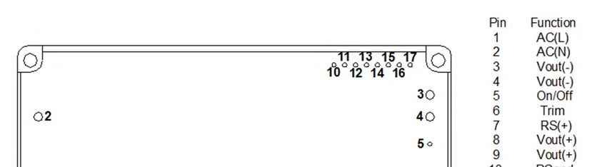
TDK-Lambda
                                                                                                                                 PFH500-SERIES
                                                                                                                           INSTRUCTION MANUAL

 1      Model Name Identification Scheme

                   PFH 500X – YZ – UVW - R
                                                                                      ROHS
                                                                                      Option Code
                                                                                      Rated Output Voltage
                                                                                      Feature Set
                                                                                      Output Power
                                                                                      Series Name

      1.1      Ordering Table

                     X                   YZ               U                  V                                         W
                                                       Case               Parallel           OVP            OCP              OTP            Pin
                Feature Set            Output
                                                      Mounting           Operation         (Default)      (Default)        (Default)       Length

          F: Full Features           12: 12 Vdc      0: Thru-Hole     0: No Load Share      Latching    Non-Latching     Non-Latching       0.240”
          A: 400 Hz Compatible*      28: 28 Vdc      1: Threaded      D: Droop Load
                                     48: 48 Vdc                          Share

                                     -UVW (OPTION CODE EXAMPLES)
                                         -000                          No Load Share
                                                      Thru-Hole
                                                                         Droop Load
                                        -0D0                               Share
                                                                                            Latching    Non-Latching     Non-Latching       0.240”
                                         -100                          No Load Share
                                                       Threaded
                                                                         Droop Load
                                        -1D0                               Share
        *400 Hz input line frequency operation currently supported in 28 V output module. Consult factory on availability of other output voltages.

REV 3.0 (January 6, 2021)                                                                                                                             5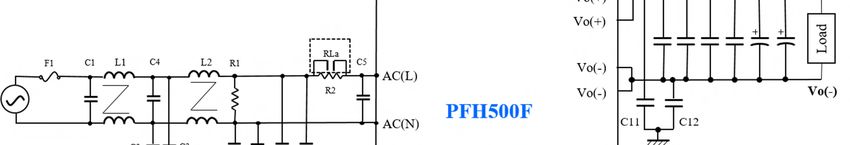
TDK-Lambda
PFH500-SERIES
INSTRUCTION MANUAL
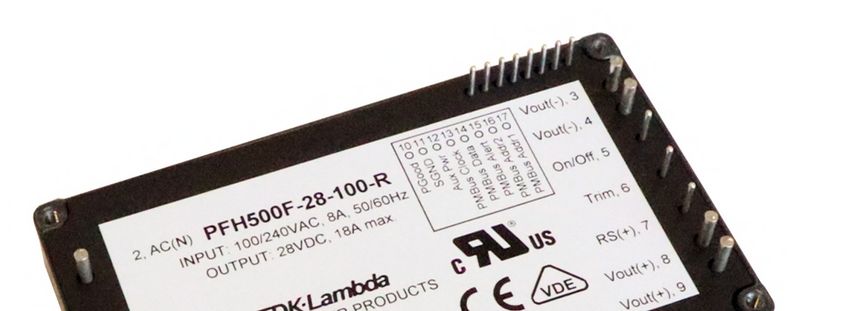
2 Module Pinout (Pin Side-Up)
PIN # PIN DESIGNATION FUNCTION PIN # PIN DESIGNATION FUNCTION
1 AC (L) AC Input - Live Line 11 SGND Secondary Signal Ground
2 AC (N) AC Input - Neutral Line 12 Aux Pwr Auxiliary Supply Output
3 Vout(-) -Output Voltage (Return) 13 PMBus Clock i2C Clock
4 Vout(-) -Output Voltage (Return) 14 PMBus Data i2C Data
5 On/Off Output On/Off Pin 15 PMBus Alert Alert Line
6 Trim Output Voltage Adjust 16 PMBus Address 2 Address Lines
7 RS(+) +Remote Sense Line 17 PMBus Address 1 Address Lines
8 Vout(+) +Output Voltage 18 Inrush Control Inrush Control pin
9 Vout(+) +Output Voltage 19 -Vbus -Boost Voltage
10 PGood Power Good 20 +Vbus +Boost Voltage
NOTE: - Module case can be connected to Frame Ground through M3 mounting hole(s).
- Spacing/clearance requirement between mounting screw and pin 20 (≥ 1 mm slot).
- Note that +VBUS and –VBUS terminals are primary voltage with high voltage rating (405 Vdc).
- Do not connect any load(s) across +VBUS and -VBUS terminals. Otherwise, it may damage the module.
REV 3.0 (January 6, 2021) 6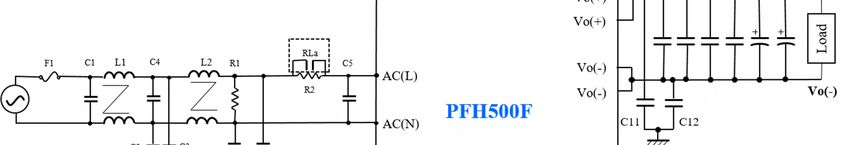
TDK-Lambda
                                                                                                                                                  PFH500-SERIES
                                                                                                                                            INSTRUCTION MANUAL

 3      Circuit Block Diagram

                                                                  PFC Circuit                  Vbus                  DC-DC Circuit

                                              Vac

                                                                                                                                            Output Filter
                                Surge Prot.

                                                                                        Bulk Caps
                   EMI Filter

                                                    Inrush                                            DC-DC
                                                                         Bridgeless                                          Synchro.
           Fuse                                     Circuit                                           Bridge                                                       Vo
                                                                         PFC Conv.                                           Rectifiers
                                                                                                      Converter
                                                                 Relay

                                                                                                                  Ipeak
                                                    Vin Detect                                                    Sense        DC-DC
                                                                         PFC                                                                            Vo_sns
                                                    UVP/OVP                                                                    Digital
                                                                         Digital
                                                                         Controller                                            Controller
                                                                                                                                                            ON/OFF
                                                                                                              Digital          (OVP/UVP)                    Trim
                                                    Iin Detect                                                Isolators
                                                    OCP1                        URT                                                                         Rs
                                                                                                                               URT
                                                                                                                                                            PG
                                                                                      Vbus
                                                       OTP1                           OVP1
                                                                                                                                                 PMBus
                                                                                      UVP2                    Bias
                                                                                                            Supplies
                                                                                                                                                            Vaux

                                                                                                                             OTP2                  Io SNS

                                   NOTE: The blocks with red font are the external components required for the operation of PFH module.

                  SWITCHING FREQUENCY

                  PFC Converter (Fixed)                                                         145 kHz

                  DC-DC Converter (Fixed)
                                     Vo = 12 Vdc                                      135 kHz (Primary)                   270 kHz (Secondary Ripple)
                                     Vo = 28 Vdc                                      145 kHz (Primary)                   290 kHz (Secondary Ripple)
                                     Vo = 48 Vdc                                      165 kHz (Primary)                   330 kHz (Secondary Ripple)

                  BIAS Converter                                                                135 kHz

REV 3.0 (January 6, 2021)                                                                                                                                                   7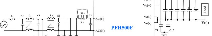
TDK-Lambda
                                                                                                                  PFH500-SERIES
                                                                                                            INSTRUCTION MANUAL

 4      Sequence Timing Diagram

                        NOTE: PFH Series product has a remote ON/OFF pin (PIN# 5) that is referenced to output return.

REV 3.0 (January 6, 2021)                                                                                                    8
TDK-Lambda
PFH500-SERIES
INSTRUCTION MANUAL
5 Terminal Connecting Method
In order to use the PFH500 series, this module must be connected with external components according to Figure 5-1. Pay
attention to the wiring details. If the PFH module is wired incorrectly, the power module may be damaged.
The PFH Series module is designed for both convection and conduction cooling applications. Use a heat sink and fan(s) to
remove the heat generated by operation at heavy loads. For selection of heat sink(s) and the heat sink heat transfer method,
refer to the Power Module Application Note.
PMBus_Clock
PMBus_Add2
PMBus_Add1
PMBus_Alert
PMBus_Data
L=50 mm
RLa
PMBus Interface
RS (+)
L1 L2 C15
Vo (+)
F1 C13
Vo (+)
Vac(L) AC (L)
R2 Vo (+)
C1 C4 R1
Input
C5 Output
Vac(N) AC (N) Vo (-)
C2 C3 Vo (-) C14 C16
PFH500F Vo (-)
C11 C12
Case
C6 C7 Trim
Earth GND
PG
ON/OFF
Input EMI Filter Aux Power
CISPR 32:2015 Class A SGND
for Class B, see Appendix
Inrush
Control -VBUS + VBUS
C9
RLb
C10
R3 R4
Fig. 5-1 Basic Connection
REV 3.0 (January 6, 2021) 9
TDK-Lambda
PFH500-SERIES
INSTRUCTION MANUAL
5.1 F1 External Input Fuse
PFH500 series module has no internal fuse. Use an external fuse to meet Safety Agency requirements.
PFH500 series modules were tested for safety agency certifications (UL, cUL, VDE, etc.) using 10A, 250 Vac, Fast-Acting
line fuse. One Fast-Acting type fuse must be used for each PFH module.
When selecting a fuse, be aware the line inrush surge current will flow through the PFH module during initial line power
application (or line power switch in). Check the I2t rating of the external power switch (or circuit breaker), and the external line
fuse to make sure that the fuse will not blow, and/or the circuit breaker will not trip.
Recommended External Fuse:10 A, 250 V (Fast Acting)
Note: Select fuse based on rated voltage, rated current and surge current capability.
(1) Voltage Ratings
100 Vac line: AC125V
200 Vac line: AC250V
(2) Current Ratings
Rated current is determined by the maximum input current based on operating conditions and can be calculated by the
following formula:
Pout
Iin (max) (Arms) (Formula 5-1)
Vin (min) η PF
Iin (max) : Maximum Input Current
Pout : Maximum Output Power
Vin (min) : Minimum Input Voltage
: Efficiency
PF : Power Factor
For Efficiency and Power Factor values, refer to separate document “PFH500F Series Evaluation Data”.
5.2 C1 (1 µF); C4 (1 µF); C5 (2.2 µF) Film Capacitor or Class X Safety Capacitor
These capacitors are connected across the lines to reduce differential mode interference. Since the X cap is connected across
the line and neutral, the current flowing through the cap can be high. When selecting X capacitor, be sure to check the
allowable maximum ripple current rating of this capacitor.
TDK-Lambda Americas recommends the customers to verify the actual ripple current flowing through each X capacitor by
measuring the current flow.
Connect C5 as close to the input terminals of PFH500 series power module [i.e. AC(L) and AC(N)] as possible.
Recommended Voltage Rating of X - Capacitors: 250 Vac or greater
REV 3.0 (January 6, 2021) 10TDK-Lambda
PFH500-SERIES
INSTRUCTION MANUAL
5.3 L1 (6.3 mH); L2 (6.3 mH) Common Mode Choke
Add recommend common mode chokes to reduce EMI noise. When using multiple PFH500 series modules in parallel, it is
important to provide EMI filtering (including X caps, Y caps, and common mode chokes) for each PFH500 module.
5.4 C2 (3300 pF); C3 (3300 pF) Ceramic Capacitor or Class Y Capacitor
Y-capacitors are used to protect against common mode noise. Be sure to consider leakage current requirement of your
equipment or instrument when selecting these capacitors.
5.5 R1 (470 k, 2 W); R3 (470 k, 2 W); R4 (470 k, 2 W)
Connect bleeder resistor, R1, across the AC input terminals and connect R3 and R4 in series across C9 and C10 as shown
in Fig. 5-1.
5.6 C6 (470 pF); C7 (470 pF) Ceramic Capacitor or Class Y Capacitor
Add these Y capacitors as an EMI common-mode noise countermeasure. Be sure to consider leakage current of your
equipment when selecting these capacitors.
Connect C6 as close as possible to AC(L) terminal. Connect C7 as close as possible to AC(N) terminal.
5.7 Electrolytic Bulk Capacitors: C9 (470 µF); C10 (470 µF)
Recommended Voltage Rating: 450 Vdc (105 ºC rated capacitor)
Recommended Capacitance: 2 x 470 µF
Notes:
1. Connecting capacitors with a higher capacitance value than mentioned could result in the PFH Series power module
being damaged. Consult TDK-Lambda for higher bulk capacitance requirement.
2. When using the PFH power modules below -20 °C ambient temperature, both AC ripple of VBUS and output ripple
voltage might be affected by ESR characteristics of the bulk capacitors. Therefore, be sure to verify characteristics by
actual evaluation.
3. Bleeder resistors, R3 & R4 (470 kΩ / 2 W), are required to be connected across C9 or C10 to discharge the bulk capacitor
voltage to a safe level after power off. Refer to Figure 5-1.
4. Do not connect any external load to the Bulk Capacitors or the module may be damaged.
REV 3.0 (January 6, 2021) 11TDK-Lambda
PFH500-SERIES
INSTRUCTION MANUAL
Selection Method of External Bulk Capacitor for VBUS
C9 & C10 capacitor values are determined by
intermediate bus voltage ripple, ripple current, and 2000
hold-up time. Select a capacitor value such that VBUS
Ripple Current (mA rms)
voltage ripple does not exceed 15 Vp-p. 1600
115 Vac
Note: When the ambient temperature is ≤ -20 ºC, the
ripple voltage of C9 & C10 will increase due to ESR 1200
characteristics. Therefore, verify above characteristics
by actual evaluation in the circuit. 800 230 Vac
For output hold-up time, refer to separate document
“PFH500 Series Evaluation Data”, and use appropriate 400
capacitor. It is recommended that actual verification
testing is performed.
0
For allowable capacitor ripple current value, refer to 0 100 200 300 400 500
Fig. 5-2. Use of a capacitor with higher ripple current Output Power (W)
rating is highly recommended.
The bulk capacitor value affects the module’s output Fig. 5-2 Allowable Ripple Current Value
hold-up time, dynamic line transient response, and
dynamic load transient response characteristics
5.8 C11 (470 pF); C12 (470 pF)
Connect Y class ceramic or film capacitors as EMI noise countermeasure to reduce high frequency noise.
Capacitors with high voltage rating are typically required since high test voltages are often applied across these capacitors
(between the output terminals and the module metal case) during Hipot testing. The metal case is connected to earth ground
or equipment frame ground (application dependent). Connect C11 as close to Vo(+) terminal as possible, and C12 as close
to Vo(-) terminal as possible.
5.9 C13 (0.1 µF, 50 V~100 V Ceramic Capacitor)
Add this output ceramic capacitor approximately 50 mm away from the PFH Series module output terminals to help reduce
high frequency output noise.
5.10 C14 (40µF, 50 V~100 V or (4) 10 µF Ceramic capacitors in parallel)
Add this output ceramic capacitor approximately 50 mm away from the PFH Series module output terminals to help reduce
the high frequency output ripple noise, and to improve the load transient response.
REV 3.0 (January 6, 2021) 12TDK-Lambda
PFH500-SERIES
INSTRUCTION MANUAL
5.11 C15; C16 – Output Electrolytic Capacitors
Connect C15 and C16 approximately 50mm from the output terminals Vo(+) and Vo(-) of the PFH Series power module to
stabilize the module operation. Note that the output noise ripple and the characteristics of the power module during input
line turn off might be affected by the ESR and ESL values of the selected electrolytic capacitors. Also, note that output
ripple voltage may vary depending on layout of the printed circuit board.
Changes in output voltage due to sudden load change or sudden input line voltage change can be reduced by increasing
external output capacitance value.
Table 5-1 Minimum External Output Capacitance for C15, C16
Module Output Voltage C15 C16
28 V 220 µF, 50 V 220 µF, 50 V
48 V 220 µF, 100 V 220 µF, 100 V
12 V 1500 µF, 25 V 1500 µF, 25 V
Note:
(1) Panasonic capacitors (EEUFC##### Series) were used during the testing process.
(2) Use low-impedance electrolytic capacitors with excellent temperature characteristics (Panasonic, Nippon Chemi-Con
LXY Series or Nichicon PM Series or equivalent rated at least 105 ºC).
(3) For module operation at ambient temperature below -20 ºC, the output ripple voltage will be affected by ESR
characteristics of the electrolytic capacitors. Therefore, output capacitance and ESR must be maintained at lower
operating temperatures.
(4) Take note of the maximum allowable ripple current of the electrolytic capacitor used. Considering sudden load current
changes, verify actual ripple current and make sure that allowable maximum ripple current of the external capacitor is
not being exceeded.
(5) If large output load steps are performed on the PFH module, it is recommended that the output capacitance be
increased, but not to exceed the maximum capacitance value. Refer to the Data Sheet.
REV 3.0 (January 6, 2021) 13TDK-Lambda
PFH500-SERIES
INSTRUCTION MANUAL
5.12 R2
By inserting a ceramic wire wound, thermal fused inrush resistor between the line filter and the input terminal, AC(L) as
shown in Fig. 5-1, the inrush current can be limited to a pre-determined level. Proper inrush control is required during turn-
on to avoid the external line fuse from being blown, the input circuit breaker from being tripped, the bulk capacitors and/or
PFH Series module internal parts from being damaged, and to prevent oscillation between the input inductor and the bulk
capacitors.
For 50 / 60 Hz operation, the maximum allowable resistance value is limited by the bulk capacitor bank charging time, and
VBUS ramp-up time. The resistance value for R2 is between 20 Ω minimum and 30 Ω maximum. A 22 Ω / 1.6 W ceramic
wire wound, thermal fused inrush resistor is typically recommended.
For 400 Hz operation, the maximum allowable resistance value is limited by the bulk capacitor bank charging time, and
VBUS ramp-up time. The resistance value for R2 is between 9.4 Ω minimum and 10Ω maximum. Two 4.7 Ω / 5 W wire
wound, fusible inrush resistor connected in series is typically recommended.
Note:
(1) PFH500 series module will not operate if this external inrush resistor is not present.
(2) For 50 / 60 Hz operations 22 Ω / 1.6 W is typically used (UCHIHASHI, Part #: A5MC-220J)
(3) For 400 Hz operations, two 4.7 Ω / 5 W resistors in series is typically used (TT ELECTRONICS,
Part #: ULW5-4R7JT075)
(4) For 400 Hz operations, R2 could be damaged if the applied input voltage exceeds maximum
input voltage rating of 135 Vac.
Selection Method of External Resistor
(1) Calculating Resistance Value for R2:
Resistance can be calculated by the formula below.
Vin _ pk
R2 (Ω ) (Formula 5-2)
Irush
R2 : Minimum Resistance Value Required for External Thermal Resistor, R2
Vin_pk : Maximum Input Voltage Peak Value = Maximum Input Voltage (rms) x 2
Irush : Allowed Input Inrush Current Peak Value during Initial Power Switch ON
(2) Required Surge Current Rating:
Sufficient surge current withstanding capability is required for external R2 thermal resistor. The required Surge Current
Rating of R2 can be determined by I2t. (Current squared multiplied by time)
Cb (Vin _ pk ) 2 2
I t
2
( A s) (Formula 5-3)
2 R2
I2t : Thermal Resistor current-squared multiplied by time rating
Cb : Maximum Boost Output Bulk Capacitance
Vin_pk : Maximum Input Voltage Peak Value = Input Voltage (rms) x 2
R2 : Resistance Value for External Thermal Resistor, R2, Chosen
REV 3.0 (January 6, 2021) 14TDK-Lambda
PFH500-SERIES
INSTRUCTION MANUAL
(3) R2 Maximum Value Limitation:
The maximum value of R2 is limited by R-C charging time. The higher the R2 value is, the lower the inrush current, but
the longer the start-up time will be (see section 6-3 discussion). PFH Series modules do not have a second inrush
event. When the ac line is switched on, the ac power source charges the bulk capacitor bank via the inrush resistor.
Once the Boost converter output voltage (or bulk capacitor voltage) reaches about 70 V, the internal bias circuitry starts
to work. After a short delay, the PFC controller starts to enable the PFC converter, which charges the bulk capacitor
bank to a regulated voltage level, about 385 V. The value of the thermal resistor, R2, limits the PFC converter ramp –
up time, especially when operating near low line.
5.13 RL Inrush Relay (12 V Coil, 10 A / 277 Vac; 16 A / 125 Vac)
An inrush relay is connected in parallel with R2 resistor. As soon as VBUS reaches the pre-set value (close to the peak of
the maximum ac line voltage), the inrush control pin will energize the relay. This method mitigates or even eliminates the
second inrush current event during the relay closing. It is very important to make sure that the relay contacts are
opened before applying AC power. Otherwise, an inrush current surge will damage the PFH Series module.
The inrush relay chosen must have a maximum switching voltage ≥ 265 Vac. A relay with minimum of 10 A / 277 Vac,
16 A / 125 Vac rating, and 12 V / (15 to 20 mA) nominal coil operating voltage and current is recommended.
Note:
(1) Panasonic relay (JVN1A-12V-F) was used during the testing process.
6 Explanation of Functions and Precautions
6.1 Input Voltage Range
PFH500F Series
Input AC voltage source should be within the ranged from 85 – 265 Vac (47-63 Hz). Connecting the PFH Series module
to any power source outside of this specified range will prevent the module from starting.
PFH500F series power module is certified by various safety agencies with a certified label indicating: 100-240 Vac, 50-
60 Hz, 8 A.
PFH500A Series
Input AC voltage source must be within the range from 85 – 135 Vac (375-420 Hz). Connecting the PFH Series module
to any power source outside of the recommended range may prevent the module from starting.
6.2 Output Voltage Adjustment Range
The output voltage of the PFH Series module can be adjusted up and down by connecting a trim resistor between Trim pin
and RS(+) pin or Vout(-) pin. Care must be taken to prevent the trim up voltage from exceeding 20% of the nominal voltage.
Otherwise, it may activate the module’s OVP protection function.
Output Voltage Adjustment Range: ±20% of the nominal output voltage setting
When trimming up the output voltage, the output current needs to be reduced to keep the maximum output power to 504 W
or less. Operating beyond the specified ratings can cause permanent damage to the power module.
The trim-up and the trim-down connections using external resistor are shown in Fig. 6-2, and Figure 6-4. If the remote sensing
feature is NOT used, the RS(+) pin needs to be connected to Vout(+) for local sensing. For details on Remote Sensing
function, refer to Sec 6.8, Remote Sensing.
REV 3.0 (January 6, 2021) 15TDK-Lambda
PFH500-SERIES
INSTRUCTION MANUAL
NOTE: Due to noisy environments, it is strongly recommended that an external 0.1 µF capacitor (Min) be placed from the
Trim pin to SGND.
Output Voltage Adjustment using external Fixed Trim Resistor
Trim Up: With a trim resistor connected between the Trim pin and Vout (+) pin, the output voltage is adjusted up. To adjust
the output voltage up a percentage of Vout (%) from Vo,nom, the trim resistor (in k) should be chosen according to the
following equation:
V0,nom (100 %) 100
Rtrim _ up 5.11 ( 2) (Formula 5-4)
Vref % %
% = 100(Vo,nom - Vdesired) / Vo_nom
Vref = 1.22 V
The trim-up resistor (Rt_up) values from +5% to +20%1, can be found in Tables 6-1. The trim-up circuit connection is shown
in Figure 6-2. Trim resistors should have +/-1% or better tolerance.
Table 6-1 External Trim-Up Resistor Value for
PFH500F – 12 – xxx PFH500F – 28 – xxx PFH500F – 48 – xxx1
% Trim-Up of Trim-Up Calculated Trim-Up Calculated Trim-Up Calculated
Vo_nom Resistance Vout Resistance Vout Resistance Vout
(Vo) (Ω) (V) (Ω) (V) (Ω) (V)
+ 5% 1034 k 12.6 V 2391.4 k 29.4 V 4092 k 50.4 V
+ 10% 540.9 k 13.2 V 1250.3 k 30.8 V 2141 k 52.8 V
+ 15% 376.7 k 13.8 V 869.8 k 32.2 V
+ 20% 294.6 k 14.4 V 679.6 k 33.6 V
NOTE1: PFH500F-48-xxx can only trim up +10%
50000
Trim Resistance in (kW)
5000
500
0 2 4 6 8 10 12 14 16 18 20
% Increase in Output Voltage, D(%)
Fig. 6-1 Trim-Up Resistance vs. Percentage Voltage Trim- Fig. 6-2 External Trim-Up Circuit Connection.
Up.
REV 3.0 (January 6, 2021) 16TDK-Lambda
PFH500-SERIES
INSTRUCTION MANUAL
Trim Down: With a resistor connected between the Trim pin and Vout (-) pin, the output voltage can be adjusted down. To
adjust the output voltage down a percentage of Vout (%) from Vo,nom, the trim resistor should be chosen according to the
following equation (in k).
100
Rtrim _ down 5.11 ( 2) (Formula 5-5)
%
The trim-down resistor (Rt_down) values for the trim-down voltage range from -5% to -20% can be found in Tables 6-2.
The trim down connection diagram is shown in Figure 6-4.
Table 6-2 External Trim-Down Resistor Value
PFH500F – 12 – xxx PFH500F – 28 – xxx PFH500F – 48 – xxx
% Trim-Down Trim-Down
Calculated Vout Calculated Vout Calculated Vout
of Vo_nom Resistance
(V) (V) (V)
(Vo) (Ω)
- 5% 92.0 k 11.4 V 26.6 V 45.6 V
- 10% 40.9 k 10.8 V 25.2 V 43.2 V
- 15% 23.9 k 10.2 V 23.8 V 40.8 V
- 20% 15.3 k 9.6 V 22.4 V 38.4 V
10000
Trim Resistance (k W )
1000
100
10
0 2 4 6 8 10 12 14 16 18 20
% Decrease in Output Voltage, (%)
Fig. 6-3 Trim-Down Resistance vs. Percentage Voltage Trim- Fig. 6-4 External Trim-Down Circuit Connection.
Down.
REV 3.0 (January 6, 2021) 17TDK-Lambda
PFH500-SERIES
INSTRUCTION MANUAL
6.3 Inrush Current
Input inrush or surge current changes with thermal fuse resistor (R2) value and the external boost converter bulk capacitance
value (C9 and C10). It is recommended that actual evaluation testing be performed to confirm the inrush current value.
The inrush current peak values shown in the specification or data sheet are measured at nominal lines (115 Vac and 230
Vac), at 25 ºC using the basic connection as shown in Figure 5-1.
The external line fuse should be chosen to handle the measured inrush peak current and based on the PFH product label. If
used in conjunction with the line fuse, circuit breakers should be selected using the same criteria.
6.4 Output Over Voltage Protection (OVP)
PFH Series modules are equipped with an OVP protection function. The OVP function activates when output voltage is greater
than the OVP trip-point. When the OVP triggers, the module output will shut down either with latch or auto-recovery depending
upon the option code specified. The standard option for PFH Series modules is a latching over voltage protection.
When the OVP function activates, cut off the input ac line power. Afterwards, verify VBUS voltage has dropped below 10 V.
Check for any abnormal conditions. Then, attempt to recover output voltage by cycling input voltage back on.
In addition, the OVP latch can also be reset by turning the module off and then on using either the On/Off pin or via PMBus
command.
The OVP set-point can be changed via PMBus. The OVP setting can only be lowered by via PMBus. The maximum allowed
output voltage is limited by the pre-defined VBUS voltage settings.
Care must be taken to avoid applying higher voltage externally to the output terminals of PFH Series module. Otherwise, it
may cause permanent damage to the module.
6.5 Boost (or VBUS) Over Voltage and Under Voltage Protection (BOVP/BUVP)
PFH Series modules monitor the VBUS voltage to protect it from both over-voltage and under-voltage operation. If a module
reaches these pre-defined protection levels, the module’s output will shut down and VBUS will also shutdown. The module
will attempt to auto-restart after the shutdown. The inhibiting time before restart depends on the value of the bulk caps and
bleeder resistor values used.
6.6 Over Current Protection (OCP)
PFH Series modules are equipped with various OCP protection functions including input PFC over-current protection, DC-
DC primary side peak cycle-by-cycle over-current protection, module over-load protection, and short circuit protection. In
normal operating conditions as specified by the specification and derating curves, the OCP protection will not be activated.
The module OCP function triggers when the output current typically exceeds 105% to 140% of maximum rated DC output
current in the specification. To reduce variation, the OCP set-point is temperature compensated, and is calibrated during the
manufacturing test process.
The module’s output will automatically recover when the over-load condition or the short circuit is removed.
For modules with non-latching OCP, the module will enter a 2-second hiccup retry sequence once an OCP condition is
detected. The module will try to re-start up to 6 times at 2-second hiccup rate. If the over-load condition remains after the
module tries to re-start up to 6 times, then it will enter a 6-minute hiccup retry sequence. Once the module enters the 6-minute
hiccup mode, it will stay there until the over-load condition is removed, and the module can operate for at least 7 minutes
without any alarms. After the 7-minute counter has cleared, the module will revert to the standard 2-second hiccup timer if a
future OCP event is detected.
REV 3.0 (January 6, 2021) 18TDK-Lambda
PFH500-SERIES
INSTRUCTION MANUAL
When the PFH Series module is operated outside the specified input voltage range, the input OCP function may be activated
to protect the module from drawing excessive input current to help guard against damage to the module.
The PFH Series OCP set-point is set to a fixed value, however it can be reduced via PMBus.
NOTE:
(1.) Certain Electronic Loads may have excessive current overshoot which can cause the PFH overcurrent protection
to engage.
(2.) Continuous short circuit or overload conditions are not recommended and might result in power supply over-heating
or damage.
6.7 Over Temperature Protection (OTP)
PFH Series modules are equipped with internal OTP protection function. There are multiple thermal sensors located in the
hotspot of the PFH module. The digital controller reads back the temperature sensed and disables the operation based on
the pre-set OTP settings. Refer to Sections 7.1 and 7.2 for the external thermal measurement location of the PFH module
and for the module’s safe operating range.
When any one of these sensors hit their temperature trigger point, the OTP protection will be activated, and the module will
shut down. The module will re-start after the internal temperature drops below the re-start point, usually 20 ºC below the trip
point. Non-latching, auto-restart OTP protection is a standard feature for PFH modules.
Note: When a module recovers from an OTP fault, the module might trip OCP during the start-up and cause a long hiccup
delay (6 Minutes). Therefore it is recommend to reduce the module’s load current to 80% of its output current rating prior to
OTP recovery.
6.8 Remote Sensing
PFH Series modules have one remote sensing terminal, RS(+), to compensate for the line drop from the output terminals to
the output load. When the remote sensing is not required, i.e. using local sensing, be sure to short RS(+) pin to the Vout(+)
pins. Note, the output line drop (the voltage drop due to long cable impedance) and voltage compensation range must fall
within the typical (50 mV) output remote sense range. At any conditions, the maximum output power of PFH module should
not be exceeded.
When using the remote sensing feature, do adequate evaluation to make sure the module does not have excessive noise or
oscillation at the load terminals. Should a noise filter inductor be inserted between Vo(+) pin(s) and the load terminal, the
RS(+) sense must be connected on the module’s side of the inductor. Some precaution in the layout may be needed. Contact
TDK-Lambda Technical Support for assistance if needed.
Voltage Stable at Load Terminals Voltage Stable at Module Output Terminals
PMBus Interface
RS (+) PMBus Interface
RS (+)
Vo(+) +
AC(L) Vo(+) +
AC(L)
Vo(+) Vout Vo(+) Vout
Load
Load
Vo(-) C15 C16
AC(N) Vo(-) C15 C16
- AC(N) -
Vo(-) Vo(-)
PFH500F PFH500F
Case Case
Trim Trim
PG PG
ON/OFF ON/OFF
Aux Power Aux Power
SGND SGND
Inrush Inrush
Control -VBUS + VBUS Control -VBUS + VBUS
Fig. 6-5 Remote Sensing is USED. Fig. 6-6 Remote Sensing is NOT USED (Local Sensing).
REV 3.0 (January 6, 2021) 19TDK-Lambda
PFH500-SERIES
INSTRUCTION MANUAL
6.9 ON-OFF Control
PFH Series modules have an ON-OFF control pin, which is used to enable (turn on) or disable (turn off) the module. When
this pin is low, the PFH module is enabled. Internally, this pin is connected to a 10 k pull-up resistor that is in series with
3.3 V source. Due to noisy environments, it is strongly recommended that an external 0.1 µF capacitor (Min) be placed from
the ON-OFF pin to SGND.
Maximum sink current of ON-OFF pin : 300 µA
Maximum low voltage for ON-OFF pin : 1V
Maximum high voltage of ON-OFF pin : 3.3 V
ON-OFF pin references to Vout(-) Signal Ground.
The digital controller inside the module will remember the ON-OFF control sequence. If the module is enabled by ON-OFF
pin, then it must be turned off by ON-OFF pin. Trying to turn off the module by PMBus will be ignored. If the module is
enabled by PMBus control, then it must be turned Off through PMBus control, the ON-OFF pin control function will be
ignored.
Various ON-OFF pin connection schemes are shown below:
PMBus Interface
RS (+)
Vo(+) +
AC(L)
Vo(+) Vout
Load
Vo(-) C15 C16
AC(N)
-
Vo(-)
PFH500F
Case
Trim
PG
ON/OFF
Aux Power
SGND
Inrush
Control -VBUS + VBUS
Fig. 6-7a ON-OFF Pin Tied Active. Fig. 6-7b ON-OFF Control Using Switch.
NOTE: Module is always On NOTE: S1 should be located next to the module
6.10 Power Good Signal (PGood)
PFH Series modules have an Open-Drain Power Good pin. The PGood pin can be used to either turn on or off load(s), or to
communicate with external controllers and signal the system regarding the status of PFH module. An external pull-up
resistor is required to limit sink current.
When the output voltage of PFH module is within the specified output voltage regulation band, the Power Good signal is
activated. An active “Low level” indicates Power Good.
Maximum sink current of Power Good pin : 150 mA
Maximum voltage of Power Good Pin : 50 V
VOUT_LOW (Max) : 1 V @ 150 mA
Some filtering (hardware and/or software) of the Power Good pin may be required for applications with large noise levels.
REV 3.0 (January 6, 2021) 20TDK-Lambda
PFH500-SERIES
INSTRUCTION MANUAL
6.11 Auxiliary Bias Power
PFH Series modules have an Auxiliary Bias Supply pin, referenced to Vout(-). This auxiliary bias is internally over-current
protected. It is capable of providing a loosely regulated 12 V bias (10 – 14 V, with 200 mA maximum current).
6.12 OPTIONAL Droop Load Share (Parallel Operation)
Droop load sharing scheme is available. The droop load share scheme senses the module’s output load current, and then
intentionally lowers the output voltage reference, which then in turns reduces the regulated output voltage as shown in Figure
6-8b.
Use of OR-ing diodes (Schottky diodes or Or-ing FETs) with same forward voltage drops and same temperature rise
characteristics is required. The use of the OR-ing diodes is to prevent any negative current from flowing back into the PFH
module(s).
In steady state and near ideal sharing, each PFH Series module will provide close to 50% of the total load current. Figure 6-
8c depicts two PFH units running at 18 A load, and then one of the units is turned off.
The load share accuracy is a function of the module’s initial output voltage setting accuracy, load current sensing accuracy,
output wiring impedance differences, and the forward voltage drop difference of the external OR-ing diodes (or OR-ing FETs).
Dual-Packaged Schottky diodes with the same forward voltage drop and temperature characteristics will help improve the
load share accuracy.
When using droop current sharing, the RS (+) needs to be connected for local sense mode, i.e. to Vo (+) pins.
Since PFH Series modules feature hiccup OCP protection scheme, in a multiple module parallel system, start-up load
current must be the same or less than one PFH module’s maximum rated current to avoid start-up problems.
It is recommended that the load is enabled after the output voltage has been established (e.g. use the Power Good feature
to enable the load). Derate load by 10% when operating in parallel.
NOTE: The Auxiliary Bias Power cannot be connected in parallel.
D1 D2
Io1 Io2
PFH500F-28-1Dx PFH500F-28-1Dx
Vo1 Vo_Load Vo2
Unit #1 Io_tot Unit #2
Load
Fig. 6-8a Droop Load Share Configuration (with OR-ing Diodes)
REV 3.0 (January 6, 2021) 21TDK-Lambda
PFH500-SERIES
INSTRUCTION MANUAL
Vo Controlled Linear Droop
Vo_nom
Vo_nom
Vo1
Vo2
0 Io1 Io2 Io_tot Io
50% of (Io_tot)
Fig. 6-8b Two PFH Modules in Droop Load Share Mode (with Fig. 6-8c Two PFH Modules running 18 A Load and then
OR-ing Diodes). one (1) PFH module turned Off.
6.13 PMBus Communication
The PFH Series module supports PMBus. This allows the host computer to communicate with the PFH module controller to
either read out, command, or set the module(s) operating parameters.
PFH Series module operating status and telemetry can be monitored over the PMBus. PMBus can also be used to modify
some of the operation parameters and/or limit settings, etc. For details, please refer to TDK-Lambda “PFH PMBus
Specification and Application Note”.
NOTE: If the PMBus feature set is utilized then an external 2200 pF capacitor should be placed from the PMBus_Add1 pin to
SGND and PMBus_Add2 pin to SGND.
Fig 6-9 PMBus Addressing Configuration
REV 3.0 (January 6, 2021) 22TDK-Lambda
PFH500-SERIES
INSTRUCTION MANUAL
6.14 Ripple and Noise
The output ripple and noise is measured in accordance with industry practices.
The output noise measurement connection can be found in the diagram shown in Figure 6-9 below.
A 0.1 µF ceramic capacitor, C13, and four (4) 10 µF ceramic capacitors, C14, are connected across the PFH module’s output
bus at a location 50 mm from the module output terminals. A 20 MHz bandwidth oscilloscope is recommended to be used to
measure peak-peak and RMS values.
Note that the measured high frequency noise spikes may vary depending on the wiring pattern of the printed circuit board,
and the contact impedance of the scope coaxial cable connection.
In general, the module’s output ripple spikes can be reduced by increasing external ceramic capacitor quantity and value.
NOTE: Noise is an RF frequency measurement that requires RF measurement techniques. Do not use flying ground leads
on oscilloscope probes. An RF connector is required for accurate measurements.
+V +
Load
-V -
50 mm RF Connector Oscilloscope
Frequency
Bandwidth
20 MHz
Fig 6-10 Output Noise or Ripple (including Spike Noise) Measurement Method.
REV 3.0 (January 6, 2021) 23TDK-Lambda
PFH500-SERIES
INSTRUCTION MANUAL
6.15 Series Operation
To increase the output voltage of a PFH Series module, it is possible to connect two or more PFH500 Series modules in
series. For two modules connected in series configuration, the connection diagrams are shown in Figure 6-10a and Figure 6-
10b. The output voltage from each module can be set (or trimmed) to different levels to form various combination of the total
output voltages. The RS(+) pin needs to be connected at local sense mode, i.e. to Vo(+) pin(s). Care must be taken when
using the ON-OFF feature in this configuration. Optocouplers or other isolated devices are needed. Contact TDK-Lambda
Customer Support for assistance.
Vout _ tot Vout1 Vout 2 (Formula 5-6)
RS (+) RS (+)
Vo(+) + Vo(+) +
PFH500F PFH500F
Vo(+) Vo(+)
Vout_1 Load #1
Vout_1
Unit #1 Unit #1
Vo(-) Vo(-)
-
Vo(-) Vo(-)
Load
Vout_tot
RS (+) RS (+)
Vo(+) Vo(+) +
PFH500F Vo(+)
PFH500F Vo(+)
Vout_2 Vout_2 Load #2
Unit #2 Unit #2
Vo(-) Vo(-)
- -
Vo(-) Vo(-)
Fig. 6-11a Series Operation #1 (Higher Output Voltage). Fig. 6-11b Series Connection #2 (Different Load with Different
Output Voltage).
REV 3.0 (January 6, 2021) 24TDK-Lambda
PFH500-SERIES
INSTRUCTION MANUAL
6.16 Isolation Resistance
The isolation resistance between the PFH Output and the module’s case typically will be 100 M with 500 Vdc applied.
PMBus Interface RS (+)
Vo(+)
Vo(+)
Vo(-)
Insulation Resistance Tester
Vo(-)
AC(L) Trim
PFH500F PG
AC(N) ON/OFF
Aux Power
SGND
Case
Inrush
Control -VBUS + VBUS
Fig 6-12 Isolation Resistance Test Method
6.17 Withstand Voltage Test (Hipot Test)
PFH Series modules are designed to withstand 2.5 kVac between input and module case, 3.0 kVac (reinforced voltage)
between input and output, and 1.5 kVdc between output and case, each for 1-minute dwell. When testing withstand voltage
(or Hipot test), set the leakage current limit of the withstand voltage tester (or Hipot tester) to 20 mA.
Be sure to apply only DC Hipot test voltages between output and case. AC test voltages between output and case may
damage PFH modules.
The applied voltage must be gradually ramped from zero-volts to preset testing level, and then gradually decreased back to
zero-volts. The ramp rate must not exceed 300 Vrms/sec and the dwell time should be 1 sec in mass production or 60 seconds
during the safety qualification test. Connect each terminal of PFH module according to the circuit diagrams as shown in Figure
6-12a, Figure 6-12b, and Figure 6-12c.
REV 3.0 (January 6, 2021) 25TDK-Lambda
PFH500-SERIES
INSTRUCTION MANUAL
PMBus Interface RS (+) PMBus Interface RS (+)
Vo(+) Vo(+)
Vo(+) Vo(+)
Vo(-) Vo(-)
Vo(-) Vo(-)
AC(L) Trim AC(L) Trim
PFH500F PG PFH500F PG
AC(N) ON/OFF AC(N) ON/OFF
Aux Power Aux Power Hipot Tester
SGND SGND
Case Case
Inrush Hipot Tester Inrush
Control -VBUS + VBUS Control -VBUS + VBUS
Fig. 6-13a Input to Case Hipot Test Method. Fig. 6-13b Input to Output Hipot Test Method.
PMBus Interface RS (+)
Vo(+)
Vo(+)
Vo( -)
DC Hipot Tester
Vo( -)
AC(L) Trim
PFH500F PG
AC(N) ON/OFF
Aux Power
SGND
Case
Inrush
Control -VBUS + VBUS
Fig. 6-13c Output to Case Hipot Test Method.
Withstand Voltage Testing with External Supporting Circuitry
The aforementioned Withstand Voltage Testing (or Hipot testing) only applies to PFH Series power module as a stand-alone unit. If
the Withstand Voltage Testing is to be performed in a system level with the supporting circuitry such as shown in Fig. 5-1, care must
be taken to check and verify the voltage rating of the selected external capacitors (and/or MOVs, and spark gaps for line surge
protection) between the Input terminals and Case, and Output terminals and Case.
Capacitor: Input terminals to Case (or Frame GND) : C2, C3, C6, C7
Capacitor: Output terminals to Case (or Frame GND) : C11, C12
REV 3.0 (January 6, 2021) 26TDK-Lambda
PFH500-SERIES
INSTRUCTION MANUAL
7 Thermal Considerations and Mounting Method
7.1 Thermal Consideration
The PFH Series module is designed for both convection and conduction cooling applications.
This product can be mounted in any orientation, but for forced convection applications, be sure to provide adequate airflow
around the power supply to avoid heat accumulation. Consider layout of surrounding components and orient the PFH such
that air flow across module is optimized.
It is recommended that this product operate when case temperature is maintained at or below the derating curves as shown
in Figure 7-2. The maximum case temperature should be 100 °C or less regardless of the input operating line voltage and/or
frequency. For any technical issues related to thermal derating, thermal test set-up, mounting, the heat sink attachment, and
use of the thermal interface material, please contact TDK-Lambda Americas for technical support.
Case temperature thermal measurement location is shown in Fig. 7-1.
Thermal Measurement
Location
Fig. 7-1 Baseplate Temperature Measuring Point.
To achieve a more rugged physical design and minimize common mode noise, the PFH Series module is constructed without
an Insulated Metal Substrate (IMS) board. Instead the PFH construction comprises of a multi-layer, heavy Cu PCB enclosed
within a 5-sided insulated case.
REV 3.0 (January 6, 2021) 27TDK-Lambda
PFH500-SERIES
INSTRUCTION MANUAL
7.2 Output Current / Case Temperature Thermal Derating
PFH500F module is derated according to Figure 7-2. Derating varies based on AC input voltage and desired case
temperature/output current.
Fig. 7-2a PFH500F-12-xxx Derating Curves.
Fig. 7-2b PFH500F-28-xxx Derating Curves.
REV 3.0 (January 6, 2021) 28TDK-Lambda
PFH500-SERIES
INSTRUCTION MANUAL
Fig. 7-2c PFH500F-48-xxx Derating Curves.
7.3 Recommended Soldering Condition
Recommended soldering temperature is as follows:
Soldering Dip : 260 ± 5 ºC, within 10 seconds
Preheat : 130 ºC
7.4 Recommended Washing Condition
After soldering, the following washing condition is recommended.
For other washing conditions, consult TDK-Lambda Americas Technical Support.
(1) Recommended washing solution
IPA (Isopropyl Alcohol)
(2) Washing method
In order to avoid penetration inside the power module, washing should be done with brush. Then, dry up thoroughly
after washing.
REV 3.0 (January 6, 2021) 29TDK-Lambda
PFH500-SERIES
INSTRUCTION MANUAL
8 Troubleshooting Guide
To ensure proper operation of the PFH module, the recommended test setup, required external components, connections and
specified test limits as described in this Instruction Manual should always be followed.
In the unlikely event that the PFH module encounters the abnormal performance behavior described below, the troubleshooting
guide maybe able to help rule out any external factors outside of the module that may be causing the abnormality.
(1) No output voltage
a. Is specified input voltage applied to the module’s input pins (Pin #1 & Pin#2)?
b. Is the Remote ON/OFF (Pin #5) pulled low or tied to SGND (Pin #11)?
c. During output voltage adjustment, is the correct fixed resistor used?
d. Is the power module attempting to re-start (hiccup mode, Refer to section 6.6)?
e. Is the output load within the range of the module under test?
f. Is the case temperature (Refer to section 7) within the specified operating temperature range of this module?
g. Does the output load current overshoot and exceed the modules current rating at startup?
h. Disconnect AC input voltage, wait 60 seconds, re-apply AC Input Voltage, then enable module?
(2) Output voltage is too high
a. Is the remote sensing terminal RS(+) correctly connected?
b. Is the measurement done at the sensing points?
c. During output voltage adjustment, is the fixed resistor used correct?
(3) Output voltage is too low
a. Is the remote sensing terminal RS(+) correctly connected?
b. Is the measurement done at the sensing points?
c. During output voltage adjustment, is the fixed resistor used correct?
d. Is there an abnormality with the output load?
(4) Load regulation or line regulation is out of specification
a. Is specified input voltage applied?
b. Are the input or output terminals firmly connected?
c. Is the measurement done at the sensing points?
d. Are the Input and Output cables properly sized?
e. Is the output capacitance within the range per Table 5-1?
(5) Large output ripple
a. Is the measurement done according to methods described in the Instruction Manual (Section 6.14)?
b. Is the recommended ceramic capacitance used?
c. Is the measuring probe contact resistance too large (dirty or greasy)?
REV 3.0 (January 6, 2021) 30TDK-Lambda
PFH500-SERIES
INSTRUCTION MANUAL
9 Warranty Period
Standard warranty is 3 years or whatever is specified on the purchasing agreement.
The following cases are not covered by warranty:
(1) Improper use like dropping products, applying excessive shock, spilling fluids on the module, etc.
(2) Operating the PFH Series module outside the specification or not following this Instruction Manual.
(3) Defects resulting from natural disaster (fire, flood, earthquake, tornado, hurricane, etc…).
(4) Unauthorized modifications or repair by the buyers/customers.
REV 3.0 (January 6, 2021) 31TDK-Lambda
PFH500-SERIES
INSTRUCTION MANUAL
10 Appendix
10.1 EMI Conducted Emissions CISPR 32:2015 Class B Recommended Values
Figure 10.1 PFH500F-12-xxx-R
C13, C14, C15,
C1, C4 1 µF Film Capacitor 10 µF Ceramic Capacitor
C16
C2, C3 3300 pF Ceramic Capacitor C17, C18 1500 µF Electrolytic Capacitor
C5 2.2 µF Film Capacitor F1 10 A, 250 V, Fast Blow
C6, C7 330 pF Ceramic Capacitor L1, L2 6.3 mH
C6A, C7A 68 pF Ceramic Capacitor R1, R3, R4 470 kΩ, 2 W
C9, C10 470 µF Electrolytic Capacitor R2 22 ohms
1 Form A relay with 10 A, 277
Vac, power rating: 12 Vdc,
C11, C12 470 pF Ceramic Capacitor RL
16.7 mA, 200 mW, High
Sensitivity
REV 3.0 (January 6, 2021) 32TDK-Lambda
PFH500-SERIES
INSTRUCTION MANUAL
Figure 10.2 PFH500F-28-xxx-R
C1, C4 1 µF Film Capacitor C17, C18 470 µF Electrolytic Capacitor
C2, C3 3300 pF Ceramic Capacitor F1 10 A, 250 V, Fast Blow
C5 2.2 µF Film Capacitor L1, L2 6.3 mH
C6, C7, C11, C12 470 pF Ceramic Capacitor R1, R3, R4 470 kΩ, 2 W
C9, C10 470 µF Electrolytic Capacitor R2 22 ohms
1 Form A relay with 10 A, 277
C13, C14, C15, Vac, power rating: 12 Vdc,
10 µF Ceramic Capacitor RL
C16 16.7 mA, 200 mW, High
Sensitivity
REV 3.0 (January 6, 2021) 33TDK-Lambda
PFH500-SERIES
INSTRUCTION MANUAL
Figure 10.3 PFH500F-48-xxx-R
C13, C14, C15,
C1, C4 1 µF Film Capacitor 10 µF Ceramic Capacitor
C16
C2, C3 3300 pF Ceramic Capacitor C17, C18 470 µF Electrolytic Capacitor
C5 2.2 µF Film Capacitor F1 10 A, 250 V, Fast Blow
C6, C7 470 pF Ceramic Capacitor L1, L2 6.3 mH
C6A, C7A 330 pF Ceramic Capacitor R1, R3, R4 470 kΩ, 2 W
C9, C10 470 µF Electrolytic Capacitor R2 22 ohms
1 Form A relay with 10 A, 277
Vac, power rating: 12VDC,
C11, C12 2200 pF Ceramic Capacitor RL
16.7 mA, 200 mW, High
Sensitivity
REV 3.0 (January 6, 2021) 34TDK-Lambda
PFH500-SERIES
INSTRUCTION MANUAL
Information furnished by TDK-Lambda is believed to be accurate and reliable. However, TDK-Lambda assumes no responsibility for
its use, nor for any infringement of patents or other rights of third parties, which may result from its use. No license is granted by
implication or otherwise under any patent or patent rights of TDK-Lambda. TDK components are not designed to be used in
applications, such as life support systems, wherein failure or malfunction could result in injury or death. All sales are subject to TDK-
Lambda’s Terms and Conditions of Sale, which are available upon request. Specifications are subject to change without notice.
REV 3.0 (January 6, 2021) 35TDK-Lambda France SAS TDK-Lambda Americas
Tel: +33 1 60 12 71 65 Tel: +1 800-LAMBDA-4 or 1-800-526-2324
france@fr.tdk-lambda.com powersolutions@us.tdk-lambda.com
www.emea.lambda.tdk.com/fr www.us.lambda.tdk.com
Italy Sales Office
Tel: +39 02 61 29 38 63
info.italia@it.tdk-lambda.com TDK Electronics do Brasil Ltda
www.emea.lambda.tdk.com/it
Tel: +55 11 3289-9599
sales.br@tdk-electronics.tdk.com
Netherlands
www.tdk-electronics.tdk.com/en
info@nl.tdk-lambda.com
www.emea.lambda.tdk.com/nl
TDK-Lambda Germany GmbH TDK-Lambda Corporation
Tel: +49 7841 666 0 Tel: +81-3-6778-1113
info.germany@de.tdk-lambda.com www.jp.lambda.tdk.com
www.emea.lambda.tdk.com/de
TDK-Lambda (China) Electronics Co. Ltd.
Tel: +86 21 6485-0777
powersolutions@cn.tdk-lambda.com
www.lambda.tdk.com.cn
TDK-Lambda Singapore Pte Ltd.
Tel: +65 6251 7211
Austria Sales Office tls.mkt@sg.tdk-lambda.com
Tel: +43 2256 655 84 www.sg.lambda.tdk.com
info@at.tdk-lambda.com
www.emea.lambda.tdk.com/at
TDK India Private Limited, Power Supply Division
Switzerland Sales Office Tel: +91 80 4039-0660
Tel: +41 44 850 53 53 mathew.philip@in.tdk-lambda.com
www.sg.lambda.tdk.com
info@ch.tdk-lambda.com
www.emea.lambda.tdk.com/ch
Nordic Sales Office
Tel: +45 8853 8086
info@dk.tdk-lambda.com
www.emea.lambda.tdk.com/dk
TDK-Lambda UK Ltd.
Tel: +44 (0) 12 71 85 66 66
powersolutions@uk.tdk-lambda.com
www.emea.lambda.tdk.com/uk
TDK-Lambda Ltd.
Tel: +9 723 902 4333
info@tdk-lambda.co.il
www.emea.lambda.tdk.com/il
C.I.S.
Commercial Support:
Tel: +7 (495) 665 2627
Technical Support:
Tel: +7 (812) 658 0463
info@tdk-lambda.ru
www.emea.lambda.tdk.com/ru
For Additional Information, please visit
https://product.tdk.com/en/power/You can also read