In situ twistable bilayer graphene - Nature
←
→
Page content transcription
If your browser does not render page correctly, please read the page content below
www.nature.com/scientificreports
OPEN In‑situ twistable bilayer graphene
Cheng Hu1, Tongyao Wu1, Xinyue Huang1, Yulong Dong1, Jiajun Chen1, Zhichun Zhang1,
Bosai Lyu1, Saiqun Ma1, Kenji Watanabe2, Takashi Taniguchi3, Guibai Xie4, Xiaojun Li4,
Qi Liang1 & Zhiwen Shi1*
The electrical and optical properties of twisted bilayer graphene (tBLG) depend sensitively on the
twist angle. To study the angle dependent properties of the tBLG, currently it is required fabrication
of a large number of samples with systematically varied twist angles. Here, we demonstrate
the construction of in-situ twistable bilayer graphene, in which the twist angle of the two
graphene monolayers can be in-situ tuned continuously in a large range with high precision. The
controlled tuning of the twist angle is confirmed by a combination of real-space and spectroscopic
characterizations, including atomic force microscopy (AFM) identification of crystal lattice orientation,
scanning near-field optical microscopy (SNOM) imaging of superlattice domain walls, and resonant
Raman spectroscopy of the largely enhanced G-mode. The developed in-situ twistable homostructure
devices enable systematic investigation of the twist angle effects in a single device, thus could largely
advance the research of twistronics.
Two-dimensional (2D) materials and the effects of their interlayer van der Waals (vdW) interaction are topics
that attracted unprecedented attentions. With the development of the transfer technique, these atomically thin
materials can be stacked layer by layer like the Lego blocks1. Due to the subtle shift of atom position and the
delicate reconstruction of the band structure, a slight variation in the twist angle of stacking may even result in
an astonishing change in the electrical and optical properties2–9. For example, electrically, only at the magic angle
(~ 1.1°), the twisted bilayer graphene (tBLG) experiences flat electronic bands and exhibits strong correlation
phenomena, such as Mott insulator10, superconductivity11, topological Chern insulator12 and f erromagnetism13.
Optically, the resonant R aman14,15 and resonant absorption16,17 of the tBLG require the energy difference of the
two van Hove singularities in the valence and conduction bands to match the excitation photon energy, thus
can only occur for specific twist angle.
The most commonly used method to fabricate a twist device is the “tear-and-stack” t echnique18,19. The short-
coming of this method is that the twist angle of devices achieved this way are not tunable any more after the
device fabrication. As a result, when studying twist angle dependent properties, one has to collect data from a
series of devices with different twist angles. However, when comparing data measured in different devices, it is
generally hard to rule out irrelevant factors and look into the pure twist angle effect. Therefore, an in-situ dynami-
cally rotatable device is highly desirable. In light of this, some rotatable-device-fabrication methods have been
developed. One is the thermal rotation m ethod20,21, where a monolayer material on the atomically flat surface can
drift and rotate to a steady state in a high-temperature annealing process. However, the thermal rotation is of less
control. This issue can be solved by a scanning tunneling microscope (STM) folding t echnique22, where a precisely
controlled STM tip is used to pick up a graphene edge and then fold it to form tBLG. Unfortunately, the rather
small sample size (of only ~ 100 nm) obtained this technique is disadvantageous for further optical or electrical
measurements. This problem was resolved by using an atomic force microscopy (AFM) manipulation technique,
where an AFM tip is used to push a micrometer-sized thick hBN gear wheel on top of a graphene monolayer to
construct twistable graphene/hBN heterostructures23,24. The success in building such large-sized heterostructures
is beneficial from two key factors. First, the thick hBN is quite rigid, which allows the manipulation of the whole
structure by using a tiny AFM tip. Second, the graphene-hBN interface is superlubricity, therefore it is feasible
to overcome the interfacial f riction25,26. However, this method can not be directly migrated to construct in-situ
tunable tBLG due to the difficulties in manipulating a large-area flexible graphene sheet with a tiny AFM tip.
Up to now, in-situ manipulation of the rotational angle in large area tBLG homostructure is still not available.
Here, we report a technique for constructing twistable homostructure devices, and show an example that the
twist angle of a bilayer graphene device can be in-situ manipulated continuously. The device contains a large piece
1
Key Laboratory of Artificial Structures and Quantum Control (Ministry of Education), Shenyang National
Laboratory for Materials Science, School of Physics and Astronomy, Shanghai Jiao Tong University,
Shanghai 200240, China. 2Research Center for Functional Materials, National Institute for Materials Science, 1‑1
Namiki, Tsukuba 305‑0044, Japan. 3International Center for Materials Nanoarchitectonics, National Institute for
Materials Science, 1‑1 Namiki, Tsukuba 305‑0044, Japan. 4National Key Laboratory of Science and Technology on
Space Microwave, China Academy of Space Technology (Xi’an), Xi’an, China. *email: zwshi@sjtu.edu.cn
Scientific Reports | (2022) 12:204 | https://doi.org/10.1038/s41598-021-04030-z 1
Vol.:(0123456789)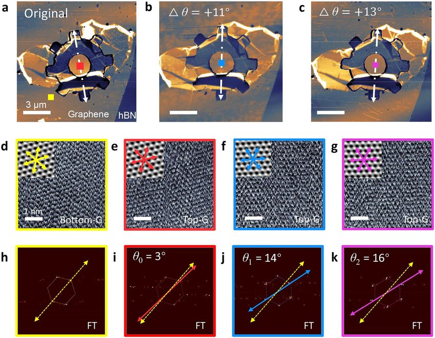
www.nature.com/scientificreports/
Figure 1. A twistable bilayer graphene device. (a) Schematic diagram of the structure of an angle-tunable
twisted bilayer graphene (tBLG) device. It consists of the two graphene monolayers separated by a hBN gear on
another hBN substrate. Moiré superlattice of period d is formed in the overlapping area in the gear center. (b)
The relation between the twist angle θ and the Moiré period d. (c) The topography of a twistable device. (d) The
tip deflection versus tip moving distance during the pushing processes of the hBN gear.
of bottom-layer graphene, a relatively smaller piece of top-layer graphene and an hBN hollow gear in between. In
the central hollow area of the gear, the top-layer graphene gets in touch with the bottom-layer graphene, forming
a region of tBLG. The gear together with the top-layer graphene can be in-situ rotated by an AFM tip, thus the
twist angle of the central region of tBLG can change accordingly. The change of the twist angle is revealed by
both the AFM identification of crystal lattice direction and the scanning near-field optical microscopy (SNOM)
imaging of the superlattice domain wall. Raman spectrum are also carried out to in-situ measure the twist angle
dependence of the device. The constructed bilayer graphene devices with in-situ dynamical tunability offer
opportunities to investigate the twist angle effects in a single device.
Results
Structure of the twistable bilayer graphene device. Figure 1a shows the schematic of our device
structure. The device consists of a large-piece of bottom-layer graphene, a small-piece of top-layer graphene,
and a preshaped hBN gear in between. The whole device is supported by another large piece of hBN flake on the
SiO2/Si substrate (see more details in Methods Section and Supplementary Information). The bottom hBN flake
is aimed at offering an atomically flat platform to avoid the surface fluctuation of the SiO2/Si substrate which
could hinder the movement of the hBN gear. The central hole of the hBN gear is designed to provide an overlap
area of two graphene monolayers to form the tBLG area. Because of the superlubricity effect between the inter-
layers of vdW materials, the friction between the hBN gear and the bottom graphene layer is low enough so that
the hBN gear is rotatable through AFM tip pushing27. The top-layer graphene, with its main part sitting on the
hBN gear, will follow the motion of the hBN gear. In this way, the twist angle θ of the central bilayer graphene
region can be controlled by rotating the hollow hBN gear with an AFM tip. Different twist angle θ leads to moiré
patterns of different periods d, as:
a
d=
2sin(θ/2) (1)
where a = 0.246 nm is the lattice constant of graphene. This relation at near zero-twist angle is explicitly shown
in Fig. 1b. The moiré superlattice period is divergent as the twist angle θ reduces to zero. This is very different
from a typical twisted heterostructure consisting of different crystals, where the maximum period is typically
finite. For instance, the maximum superlattice period of a graphene/hBN heterostructure is around 15 nm28.
This feature gives homostructure a capability of band control in a larger range.
Figure 1c shows the topography of a device scanned by tapping-mode AFM. The bright area indicates the
shape of an hBN gear with thickness ~ 140 nm, ensuring its rigidity. On the contrary, the graphene monolayer is
only 0.34 nm, and therefore is hard to see from the topography image. Thanks to the strong infrared response of
Scientific Reports | (2022) 12:204 | https://doi.org/10.1038/s41598-021-04030-z 2
Vol:.(1234567890)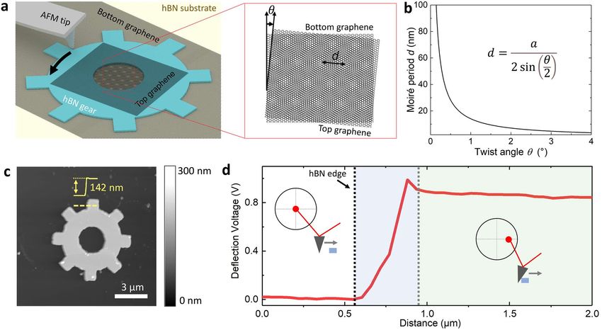
www.nature.com/scientificreports/

                                 Figure 2.  Manipulation of the twist angle. (a–c) Near-field infrared imaging of the same device at different
                                 twist angles. Δθ indicate the angle change of the hBN gear relative to its original orientation. Scale bar: 3 μm.
                                 The dashed line arrows indicate a representative direction of the hBN gear. (d) High-resolution AFM image
                                 of the bottom layer graphene. Scale bar: 1 nm. The arrows indicate the zigzag direction of the graphene lattice.
                                 (e–g) High-resolution AFM images of the top layer graphene in the colored square regions in (a–c). (h–k) The
                                 2D Fourier transform of figures (d–g). The twist angle θ between the bottom (yellow) and the top (others) layer
                                 graphene are 3°, 14°, 16°, respectively.

                                 the Dirac electrons in graphene, an infrared SNOM system with a laser beam at 10.6 μm can easily identify the
                                 graphene layers in our device (Fig. 2a–c).

                                 Procedure of AFM‑tip manipulation of the twist angle. We now introduce how to rotate the top-
                                 layer graphene using an AFM tip. The AFM tip is to exert a planar force on the hBN gear’s protrusions to rotate
                                 the hBN gear and the top-layer graphene. To ensure this works, two conditions need to be fulfilled. First, the
                                 hBN gear can move and rotate relative to the underneath bottom-layer graphene. This is achievable due to the
                                 ultra-low friction between the hBN and graphene. Note that the bottom layer graphene should be large enough
                                 so that it can stick to the bottom hBN substrate and not rotate together with the hBN gear. Second, the top layer
                                 graphene should rotate together with the hBN gear. This can be achieved by considering two aspects: (1) increase
                                 the top-surface roughness of the hBN gear. Luckily, after the lithography and etching process (over etched), the
                                 surface of the hBN gear is quite rough, which favors the top graphene to follow exactly the movement of hBN
                                 gear. (2) Choose a small size top-layer graphene sheet to reduce the graphene-graphene contact area outside the
                                 hBN gear.
                                     We use the lift-mode of the AFM to realize the rotation, where the tip first line-scans the protrusion and then
                                 pushes the protrusion by rescanning the line. During the second scan, the tip lifts down by ~ 1 μm to ensure the
                                 tip keeps contacting with the hBN gear throughout the pushing process. The AFM tip deflection signal in this
                                 process is recorded in Fig. 1d. Three different regimes of the pushing are identified: (1) As the tip lifts down and
                                 drags along the bottom graphene surface, tip-substrate friction results in a small and steady-state tip deflection.
                                 We refer to this as the substrate friction regime. (2) When the tip encounters the edge of a gear protrusion, sudden
                                 increase of mechanical resistance induces a torque to the AFM tip as well as an increase of tip deflection signal.
                                 If the tip pushing force is smaller than the maximum static friction force, the hBN gear will keep standing still.
                                 We refer to this stage as static friction regime. (3) Once the hBN gear starts to move, the friction force between
                                 the top structure and bottom graphene layer reduces from the maximum static friction to the kinetic friction,
                                 which causes the tip deflection to relax down slightly. We refer to this stage as kinetic friction regime. The dis-
                                 tance that the AFM tip moves in the kinetic friction regime corresponds to the exact motion of the hBN gear.
                                     To confirm the rotation of the hBN gear and the top-layer graphene, we carried out SNOM and high-reso-
                                 lution AFM measurements before and after each pushing process. Near-field infrared images of three states of
                                 the hBN gear is shown in Fig. 2a–c. The dashed line arrows indicate a representative direction of the hBN gear,

Scientific Reports |   (2022) 12:204 |                https://doi.org/10.1038/s41598-021-04030-z                                                     3

                                                                                                                                              Vol.:(0123456789)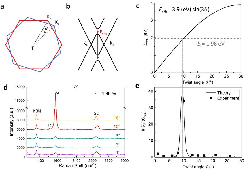
www.nature.com/scientificreports/

                                           Figure 3.  Large-range tuning of the twist angle to find the critical angle for resonant Raman. (a) The first
                                           Brillouin zone (BZ) of twisted bilayer graphene misoriented by θ. (b) Electronic bands in the vicinities of two
                                           Dirac cones. Van Hove singularities (vHs) are induced by band overlap. (c) Energy difference of the two vHs
                                           versus the twist angle θ. The gray dashed line indicates the excitation laser energy EL = 1.96 eV in our Raman
                                           measurement, corresponding to a twist angle of ~ 10°. (d) Raman spectra of a twistable bilayer graphene devices
                                           at a few representative twist angles. At θ = 10°, the graphene G-peak is largely enhanced. (e) The normalized
                                           graphene G-peak intensity as a function of the twist angle θ. Large enhancement at θ = 10° corresponds to the
                                           predicted resonant Raman.

                                           from which one can clearly see the rotation of the hBN gear relative to the stationary bottom-layer graphene.
                                           The rotation angles Δθ of the hBN gear are measured to be 11° and 13°, respectively.
                                               Furthermore, we are able to obtain the lattice orientation of both the bottom- and the top-layer graphene
                                           through high-resolution lateral force AFM, from which the twist angle can be directly obtained. We first scan
                                           the lattice orientation of the bottom-layer graphene. The scanning position is marked with a yellow square in
                                           Fig. 2a, and the scanned lattice image is shown in Fig. 2d. To see the lattice orientation more clearly, we performed
                                           Fourier transformation (FT) of the lattice image, as shown in Fig. 2h, in which the yellow arrow indicates one of
                                           the zigzag directions in the reciprocal space. The FT filtered clean lattice is displayed as an inset of Fig. 2d, and
                                           the three yellow arrows indicate the zigzag directions of the bottom layer graphene. The lattice images of the
                                           top-layer graphene in the center of the gear and their FTs are shown in Fig. 2e–g, i–k. Thus, the twist angle θ for
                                           the three states are extracted to be 3°, 14°, 16°, respectively, from Fig. 2i–k.
                                               The changes of twist angle are 11° and 13° respectively, after the two pushing manipulations, matching exactly
                                           the rotation angle of the hBN gear, in the high-resolution AFM image. The perfect match between the gear
                                           rotation angles and the change of twist angle reflects that the rotation of the top-layer graphene follows exactly
                                           the rotation of the hBN gear. This is crucial to the twist angle control and beneficial to its further applications.
                                           In the following two experiments, we demonstrate the application of both large-range tuning and small-range
                                           fine-tuning of the twist angle in finding resonant Raman and control of moiré superlattice period.

                                           Large‑range tuning of the twist angle to find the critical angle for resonant Raman. The AFM-
                                           tip manipulation of the hBN gear allows tuning of the twist angle in a large range without limitation, which can
                                           be used to find the critical angles for the transitions of some physical properties. Thanks to the micrometer-scale
                                           size, our device is applicable to far-field optical measurement. As an example, we demonstrate large-range tun-
                                           ing of the twist angle to find the critical angle for resonant Raman. Recent theoretical and experimental works
                                           have reported the presence of van Hove singularities (vHs) in the density of π electron states in tBLG. These vHs
                                           induce very strong enhancement in the Raman G band intensity. The enhancement only occurs at specific twist
                                           angle θ for a given incident laser energy EL. For two graphene layers misoriented by angle θ, the Brillouin zones
                                           of the two layers also rotationally shift by θ, as shown in Fig. 3a. Band-structure modifies most where the Dirac

          Scientific Reports |   (2022) 12:204 |                https://doi.org/10.1038/s41598-021-04030-z                                                    4

Vol:.(1234567890)
www.nature.com/scientificreports/
cones of top and bottom layers crossed. Figure 3b shows the simplified electronic band-structure in the vicinity
of the cross of these two Dirac cones. In this region, the density of states (DOS) of double-layer graphene exhibits
vHs. The energy difference between conduction and valence vHs scales with the rotational angle, EvHs = 3.9(eV)
sin(3θ), as shown in Fig. 3c. The resonant Raman occurs when excitation energy EL = EvHs. In our Raman meas-
urement, the excitation energy EL = 1.96 eV (633 nm in wavelength), which requires a twist angle around 10° for
the resonant Raman.
With a twistable bilayer graphene device introduced above, we in-situ tune its twist angle in a large range
from 0 to 30 degrees, and record its Raman spectra. Figure 3d shows Raman spectra at a few representative twist
angles, 1°, 3°, 6°, 10° and 16°. In the spectra, three main Raman peaks can be observed. The left peak around
1370 cm−1 is the hBN in-plane phonon peak, which is largely constant and therefore can be used to normalize
the Raman intensity of graphene with different twist angle. The right broad peak around 2650 cm−1 is the 2D
peak of the tBLG. The peak around 1580 cm−1 is the G peak of tBLG. The intensity of the G peak is significantly
enhanced when the twist angle is around 10° as expected from resonant Raman condition EL = EvHs. The quantita-
tive enhancement factor of the G peak of the tBLG relative to the single
layer graphene can be described
2 using
29
a second order time-dependent perturbation t heory , as I GI(G tBLG )
=
(EL −EvHs −iγ )(EL −EvHs −ℏωG −iγ )
, where ℏωG
M
single
is the energy of the G phonon, M is the product of the matrix elements for electron-photon and electron–phonon
interactions, and γ is the resonance window width. This equation can well describe the G peak intensity observed
experimentally for different twist angles, as shown in Fig. 3e. Other twist angle dependent Raman parameters,
such as the peak shift and full width half maximum (FWHM), can be found in Fig. S3.
The advantage of our technique is that we can in-situ tune the twist angle and obtain twist angle dependence
in a single device, which can largely reduce the amount of experimental workload. In addition, we can exclude
the influence from different samples and substrate factors and obtain pure twist angle dependent information.
The demonstrated method can also be used for investigation of other twist angle dependent optical properties,
such as photoluminescence, second harmonic generation, photocurrent, and circular dichroism.
Small‑range fine‑tuning of the twist angle to control the moiré superlattice period. Our in-
situ twist technique not only exhibits tuning ability in a wide range, but also shows unprecedented high preci-
sion. Since the moiré period of tBLG diverges at zero twist angle, the period is extremely sensitive to the twist
angle near the zero twist. Therefore, the control of the moiré period requires precise tuning of the tiny twist angle
near zero. Here, we demonstrate control of the moiré period of tBLG using a combination of AFM and SNOM
characterizations.
The long-wave moiré pattern of small-angle tBLG can be directly imaged with a SNOM setup. When the twist
angle θ is smaller than the critical angle of the lattice reconstruction (θc ≈ 1°), lattice reconstruction becomes
significant30. Figure 4a shows the schematic diagram of crystal lattice of small-twist angle bilayer graphene after
the atomic reconstruction (See more details of molecular dynamics simulations in the Supplementary Informa-
tion). The atoms in the reconstructed crystal form a tessellation of triangular domains that alternate with AB- and
BA-stacking, and shear domain walls are formed between the AB and BA domains. The sudden change of the
optical conductivity in the domain wall gives rise to the reflection of plasmon polariton that can be detected by
a SNOM system. As an example, Fig. 4b shows near-field optical image of a heavily doped tBLG, from which
periodically arranged AB and BA domains and domain walls can be clearly seen, in which the applied gate volt-
age is 50 V, and the corresponding charge density is about 1.5 × 1012 cm−2. Based on the imaged moiré period,
the twist angle can be derived using Eq. (1).
In Fig. 4c–f, we show a series of moiré patterns of a twistable tBLG device. Initially, the moiré period of this
device is ~ 25 nm (Fig. 4c), corresponding to a twist angle of ~ 0.6°. Then we purposely reduce the twist angle of
the device step by step with the AFM-tip manipulation. After the first manipulation, the moiré period increases
to ~ 45 nm, corresponding to a reduced twist angle of ~ 0.3°. A second fine tuning raises the moiré period up
to ~ 170 nm and decreases the twist angle to ~ 0.1°, and a third fine tuning further increases the moiré period
to ~ 250 nm and decreases the twist angle to ~ 0.05°. In addition, an inhomogeneity in the twist angle can be
observed in the small-twist-angle devices, which also commonly appeals in the direct dry-transferred tBLG
devices. In Fig. 4f, the shortest and longest periods are 195 nm and 250 nm, respectively, and the corresponding
twist angles are 0.07° and 0.05°, from which an inhomogeneity of 0.02° can be extracted. Note that the blurred
near-field infrared signal in Fig. 4c–f is due to the low initial doping level of this device. The initial doping may
originate from adsorption of polar molecules on the graphene surface. This example demonstrates that the preci-
sion of our twist angle tuning can reach 0.1°.
Discussion
In conclusion, we demonstrate construction of in-situ twistable bilayer graphene, in which the twist angle of the
two graphene monolayers can be in-situ tuned continuously in a large range with high precision. This technique
should be applicable to other 2D materials, such as, transition metal dichalcogenide (TMD), black phospho-
rus, and α-MoO3. Our findings enable systematic investigation of the twist angle effects in a single device with
largely reduce workload. In addition, the developed large-range and precise tuning of twist angle can help to
discover critical transition phenomena that depends sensitively on the twist angle. Besides, the demonstrated
in-situ tunable moiré superlattices hold potential for exploring the evolution of the correlated phenomena in
near magic angle devices.
Scientific Reports | (2022) 12:204 | https://doi.org/10.1038/s41598-021-04030-z 5
Vol.:(0123456789)www.nature.com/scientificreports/
Figure 4. Tuning the moiré period through fine adjustment of the twist angle. (a) Schematic of twisted bilayer
graphene after atomic reconstruction. (b) Near-field infrared image of a typical twist bilayer graphene at high
doping level. (c–f) A series of near-field infrared images of a twistable device at slightly different twist angles,
showing a systematically increase of the moiré period. This is achieved by fine tuning of the twist angle using
AFM tip. Scale bar: 100 nm.
Methods
Sample fabrication. The hBN substrate was mechanically exfoliated on the silica substrate. The hBN gear
and graphene were transferred onto the hBN substrate one by one by the dry transfer methods. After each trans-
fer steps, the sample was annealed in the hydrogen plasma at the temperature of 300 °C to get rid of the adhesive
residues. The power of the plasma was 30 W and the flow of H
2 was 35 SCCM with a pressure of about 47 Pa. The
distance between our sample and the center of the coil was about 45 cm.
Infrared nano‑imaging. Our home-made scattering-type SNOM setup was based on a commercial AFM
(Bruker Innova). A beam of C O2 laser of 10.6 μm wavelength was illuminated onto a gold-coated AFM tip,
which generated a near-field hot spot at the nanometer-scale tip apex. Such a largely confined hot spot could
provide extra momentum and excite plasmons in graphene. The excited plasmons propagated and reflected at
the graphene edges. The reflected plasmons modulated the local field at the tip apex and changed the light scat-
tered by the tip an MCT detector placed in the far field recorded the scattering light intensity as the AFM tip
scanned over the graphene. In order to suppress background scattering from the cantilever and the sample, the
tip vibrated vertically with an amplitude of ~ 50 nm at a frequency of about 100 kHz, and the detector signal was
demodulated at a higher order harmonic frequency by a lock-in amplifier (Zurich Instruments, HF2LI).
Received: 21 October 2021; Accepted: 14 December 2021
References
1. Guo, H. W., Hu, Z., Liu, Z. B. & Tian, J. G. Stacking of 2D materials. Adv. Func. Mater. 31(4), 2007810 (2021).
2. Sunku, S. et al. Photonic crystals for nano-light in moiré graphene superlattices. Science 362(6419), 1153–1156 (2018).
3. Yao, K. et al. Enhanced tunable second harmonic generation from twistable interfaces and vertical superlattices in boron nitride
homostructures. Sci. Adv. 7(10), eabe8691 (2021).
4. Pezzini, S. et al. 30-twisted bilayer graphene quasicrystals from chemical vapor deposition. Nano Lett. 20(5), 3313–3319 (2020).
Scientific Reports | (2022) 12:204 | https://doi.org/10.1038/s41598-021-04030-z 6
Vol:.(1234567890)www.nature.com/scientificreports/
5. Yin, L. J. et al. Landau quantization and Fermi velocity renormalization in twisted graphene bilayers. Phys. Rev. B 92(20), 201408
(2015).
6. Utama, M. I. B. et al. Visualization of the flat electronic band in twisted bilayer graphene near the magic angle twist. Nat. Phys.
17(2), 184–188 (2021).
7. Patel, H., Huang, L., Kim, C.-J., Park, J. & Graham, M. W. Stacking angle-tunable photoluminescence from interlayer exciton states
in twisted bilayer graphene. Nat. Commun. 10(1), 1–7 (2019).
8. Liu, X. et al. Tunable spin-polarized correlated states in twisted double bilayer graphene. Nature 583(7815), 221–225 (2020).
9. Polshyn, H. et al. Large linear-in-temperature resistivity in twisted bilayer graphene. Nat. Phys. 15(10), 1011–1016 (2019).
10. Cao, Y. et al. Correlated insulator behaviour at half-filling in magic angle graphene superlattices. Nature 556(7699), 80–84 (2018).
11. Cao, Y. et al. Unconventional superconductivity in magic-angle graphene superlattices. Nature 556(7699), 43–50 (2018).
12. Wu, S., Zhang, Z., Watanabe, K., Taniguchi, T. & Andrei, E. Y. Chern insulators, van Hove singularities and topological flat bands
in magic-angle twisted bilayer graphene. Nat. Mater. 20, 1–7 (2021).
13. Sharpe, A. L. et al. Emergent ferromagnetism near three-quarters filling in twisted bilayer graphene. Science 365(6453), 605–608
(2019).
14. Kim, K. et al. Raman spectroscopy study of rotated double-layer graphene: Misorientation-angle dependence of electronic structure.
Phys. Rev. Lett. 108(24), 246103 (2012).
15. Carozo, V. et al. Resonance effects on the Raman spectra of graphene superlattices. Phys. Rev. B 88(8), 085401 (2013).
16. Yu, K. et al. Gate tunable optical absorption and band structure of twisted bilayer graphene. Phys. Rev. 99(24), 2414051–2414056
(2019).
17. Havener, R. W., Liang, Y., Brown, L., Yang, L. & Park, J. Van Hove singularities and excitonic effects in the optical conductivity of
twisted bilayer graphene. Nano Lett. 14(6), 3353–3357 (2014).
18. Kim, K., Yankowitz, M. A., Fallahazad, B., Kang, S. & Tutuc, E. Van der Waals heterostructures with high accuracy rotational
alignment. Nano Lett. 16(3), 1989–1995 (2016).
19. Yankowitz, M. et al. Tuning superconductivity in twisted bilayer graphene. Science 363(6431), 1059–1064 (2019).
20. Feng, X., Kwon, S., Park, J. Y. & Salmeron, M. Superlubric sliding of graphene nanoflakes on graphene. ACS Nano 7(2), 1718–1724
(2013).
21. Wang, D. et al. Thermally induced graphene rotation on hexagonal boron nitride. Phys. Rev. Lett. 116(12), 126101 (2016).
22. Chen, H. et al. Atomically precise, custom-design origami graphene nanostructures. Science 365(6457), 1036–1040 (2019).
23. Ribeiro-Palau, R. et al. Twistable electronics with dynamically rotatable heterostructures. Science 361(6403), 690–693 (2018).
24. Finney, N. R. et al. Tunable crystal symmetry in graphene–boron nitride heterostructures with coexisting moiré superlattices. Nat.
Nanotechnol. 14(11), 1029–1034 (2019).
25. Li, J., Li, J., Jiang, L. & Luo, J. Fabrication of a graphene layer probe to measure force interactions in layered heterojunctions.
Nanoscale 12(9), 5435–5443 (2020).
26. Song, Y. et al. Robust microscale superlubricity in graphite/hexagonal boron nitride layered heterojunctions. Nat. Mater. 17(10),
894–899 (2018).
27. Qu, C., Wang, K., Wang, J., Gongyang, Y. & Zheng, Q. Origin of friction in superlubric graphite contacts. Phys. Rev. Lett. 125(12),
126102 (2020).
28. Yankowitz, M. et al. Emergence of superlattice dirac points in graphene on hexagonal boron nitride. Nat. Phys. 8(5), 382–386
(2012).
29. Sato, K., Saito, R., Cong, C., Yu, T. & Dresselhaus, M. S. Zone folding effect in Raman G-band intensity of twisted bilayer graphene.
Phys. Rev. B: Condens. Matter 86(12), 2757–2764 (2012).
30. Yoo, H. et al. Atomic and electronic reconstruction at the van der Waals interface in twisted bilayer graphene. Nat. Mater. 18(5),
448–453 (2019).
Acknowledgements
This work is sponsored by National Natural Science Foundation of China (11774224, 12074244 and 61701394)
and by “Shuguang Program” supported by Shanghai Education Development Foundation and Shanghai
Municipal Education Commission. Z.S. acknowledges support from SJTU No. 21X010200846. K.W. and T.T.
acknowledge support from the Elemental Strategy Initiative conducted by the MEXT, Japan, Grant Number
JPMXP0112101001, JSPS KAKENHI Grant Number 19H05790 and A3 Foresight by JSPS. We would also like
to thank the Centre for Advanced Electronic Materials and Devices (AEMD) of Shanghai Jiao Tong University
(SJTU) for the support in device fabrication.
Author contributions
Z.S. and C.H. conceived this project. C.H., T.W., X.H., Y.D., Z.Z. and B.L. prepared the samples. C.H., X.H.
and T.W. performed the near-field infrared measurements. C.H. carried out high-resolution AFM imaging and
Raman spectrum. J.C. carried out the molecular dynamic simulation. K.W. and T.T. provided the hBN crystals.
C.H., T.W., X.H., Y.D., Z.Z., J.C., B.L., S.M., G.X., X.L., Q.L. and Z.S. analyzed the data. C.H. and Z.S. wrote the
paper with inputs from all authors.
Competing interests
The authors declare no competing interests.
Additional information
Supplementary Information The online version contains supplementary material available at https://doi.org/
10.1038/s41598-021-04030-z.
Correspondence and requests for materials should be addressed to Z.S.
Reprints and permissions information is available at www.nature.com/reprints.
Publisher’s note Springer Nature remains neutral with regard to jurisdictional claims in published maps and
institutional affiliations.
Scientific Reports | (2022) 12:204 | https://doi.org/10.1038/s41598-021-04030-z 7
Vol.:(0123456789)www.nature.com/scientificreports/
Open Access This article is licensed under a Creative Commons Attribution 4.0 International
License, which permits use, sharing, adaptation, distribution and reproduction in any medium or
format, as long as you give appropriate credit to the original author(s) and the source, provide a link to the
Creative Commons licence, and indicate if changes were made. The images or other third party material in this
article are included in the article’s Creative Commons licence, unless indicated otherwise in a credit line to the
material. If material is not included in the article’s Creative Commons licence and your intended use is not
permitted by statutory regulation or exceeds the permitted use, you will need to obtain permission directly from
the copyright holder. To view a copy of this licence, visit http://creativecommons.org/licenses/by/4.0/.
© The Author(s) 2022
Scientific Reports | (2022) 12:204 | https://doi.org/10.1038/s41598-021-04030-z 8
Vol:.(1234567890)You can also read