DP-D Gen2 Series High Power Laboratory Power Supplies User's Manual - DSC-Electronics
←
→
Page content transcription
If your browser does not render page correctly, please read the page content below
DP-D Gen2 Series User’s Manual
Version 25.02.2021

            DP-D Gen2 Series
   High Power Laboratory Power Supplies
              User’s Manual
                     by DSC-Electronics Germany • Georgstraße 36 • 53111 Bonn

                            DSC-Electronics Germany • Georgstraße 36 • 53111 Bonn
                            DSC-Electronics Germany • Georgstraße 36 • 53111 Bonn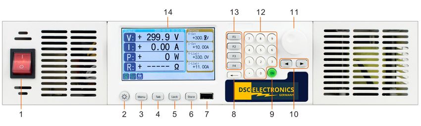
DP-D Gen2 Series User’s Manual
Version 25.02.2021

1. Connection

Our devices are pre-configured to the power grid chosen with order (if not specified otherwise, our devices are
manufactured for the EU power grid 230V 50Hz / 400V 50Hz). Subsequent adjustment after delivery is not possible.
Connecting the device to an unsuitable power source will void any warranty.

Note: Devices of the DP-D series in the performance class 4.000W - 9.000W can cause a high starting current when
switched on. Therefore, the use of circuit breakers of classes C, D or K is recommended.

                                              1 Phase / EU Power Grid
Voltage (Recommended)                                    230V ± 10% AC
Voltage (Max.)                                           250V AC
Frequency                                                50Hz - 60Hz
                                                         The maximum current of the device shall be determined as
                                                         follows:
Circuit breaker minimum requirements
                                                        I = (maximum power of the device / 230) + 2
                                           1 Phase / American Power Grid
Voltage (Recommended)                                   115V ± 10% AC
Voltage (Max.)                                          130V AC
Frequency                                               50Hz - 60Hz
                                                        The maximum current of the device shall be determined as
Circuit breaker minimum requirements                    follows:
                                                        I = (maximum power of the device / 115) + 4

                                       3 Phase / EU Power Grid (TN-S Network)
Voltage (Recommended)                                    380V - 410V
Voltage (Max.)                                           430V
Frequency                                                50Hz
                                                         The maximum phase current of the device shall be
                                                         determined as follows:
Circuit breaker Minimum requirements
                                                         I = ((maximum power of the device / 400) / 1,73) + 2

                            DSC-Electronics Germany • Georgstraße 36 • 53111 Bonn
                            DSC-Electronics Germany • Georgstraße 36 • 53111 Bonn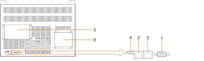
DP-D Gen2 Series User’s Manual
Version 25.02.2021
2. General
Please read through and understand this Operation Manual before operating the product. After reading always keep
the manual nearby so that you may refer to it as needed. When moving the product to another location, be sure to
bring the manual as well.
Calibration
Before shipment, the instrument has been calibrated carefully in our factory. The calibration procedures and
standards are compliant to the national regulations and standards for electronic calibration. If you have requested a
certificate with your order, this is enclosed with your device. With ordered off-site calibration (DaKKS) the calibration
was not performed in-house, please refer to the laboratory calibration protocol for details.
Warranty
We guarantee that the instrument has undergone a strict quality test before shipment and has passed all prescribed
functional tests. We provide our customers with a warranty period of three years from receipt of the device. During the
warranty period, all repairs, as well as spare parts are always free of charge. The warranty is void in the case of
defects which have been caused by user's fault, or in case of unauthorized opening.
2.1 Safety instructions
This chapter contains important safety instructions that you must follow when operating the instrument and when
keeping it in storage. Read the following before any operation to insure your safety and to keep the device in a proper
condition.
Safety symbols
The following safety symbols may appear in this manual or on the instrument:
Identifies conditions or practices that could result in injury or
WARNING
loss of life.
Identifies conditions or practices that could result in damage to
CAUTION
the instrument or to other properties.
DANGER High Voltage
ATTENTION Refer to the Manual
Protective Earth (PE)
Earth (Ground)
2.2 Safety guidelines
Please follow the safety guidelines when using and putting the device into operation in order to prevent safety risks
and to ensure the correct operation of the product.
Before connecting the device to the local power supply, make sure that the device is switched off.
Check if the product is compatible with the local power supply before connecting it.
Be careful on the correct earthing of the device (PE connection)
Do not use the product in humid environments
Do not touch the output terminals of the product with unprotected hands while it is switched on.
Do not use the device in extremely dusty rooms
Do not use the device outside the parameters specified in the data sheet
DSC-Electronics Germany • Georgstraße 36 • 53111 Bonn
DSC-Electronics Germany • Georgstraße 36 • 53111 Bonn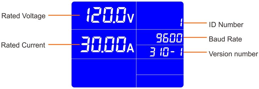
DP-D Gen2 Series User’s Manual
Version 25.02.2021

2.3 Unpacking and examination

Our products are delivered carefully packed in cardboard boxes or in wooden crates, depending on place of
destination and the type of the device (dimensions, weight). We pay attention to the environmental compatibility of the
upholstery and packaging materials used and ask you to dispose the filling material correctly if present.

Please unpack the device and check the packaging as well as the product for transport damage. Should you notice
any damage to the packaging or the device, we ask you to log it with photos and inform us immediately.

ATTENTION: If the device has been delivered in a wooden box, please do not dispose it as it can be used for eventual
return transport for service procedures. Also the packaging material of smaller devices can be stored in order to be
used if necessary for a return transport.

3. Product description

The DP-D Gen2 power supply can operate in constant voltage (CV) or constant current (CC) mode within the rated
output range. This allows continuous switching between the modes in response to the load change.

In CV mode, a regulated output voltage is provided. The output voltage remains constant as the load increases while
the output current changes in response to the load changes, until the preset current limit is reached. At that point, the
output current becomes constant and the output voltage drops in proportion to the further increases in load. The
current mode is indicated on the front panel display in area 12.

Similarly in CC mode switching from CC to CV mode automatically occurs from a decrease of the load. A regulated
output current is provided. The output current remains constant as the load decreases while the output voltage
changes in response to the load changes.

3.1 Capacitive load

Note: Can be ignored for devices with optional capacitive reverse current protection.

In the basic version, power supplies of the DP-D Gen2 series are not protected against reverse currents, which can
lead to a reverse current from the capacitive load after switching off the output voltage of the power supply. Never
connect pre-charged capacities to the power supply unit unless you have connected a serial protection diode between
the load and the power supply. The protection diode is always recommended for operation with large capacities,
please pay attention to a correct dimensioning.

3.2 Pulse load

Even if the peak current of the load is within the output power of the power supply, a high pulse load can cause
voltage fluctuations. To compensate these voltage fluctuations, expand your circuit by a serial induction. For low
currents, you can add a capacity in parallel for an even better result ( 1000uF / 1A).

                              DSC-Electronics Germany • Georgstraße 36 • 53111 Bonn
                              DSC-Electronics Germany • Georgstraße 36 • 53111 Bonn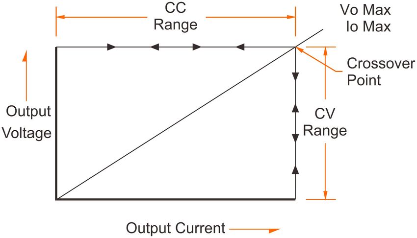
DP-D Gen2 Series User’s Manual
Version 25.02.2021
3.3 Inductive load
Note: Can be ignored for devices with optional inductive reverse current protection.
If the power supply is used with large inductive loads, voltage spikes with an amplitude of up to 5 times the output
voltage can occur, this may damage the power supply or lead to unstable operation. To protect the power supply from
damage, a freewheeling diode has to be used in parallel with the load.
3.4 Switches
If a mechanic switch is used to connect or disconnect the power supply from the load, electric discharge can occur
during switching on currents over 100A. This may cause unstable output. To prevent this behaviour, connect a RC
circuit to the switch contact point.
4. Front panel description
4.1 DP-D Gen2 front and rear panel
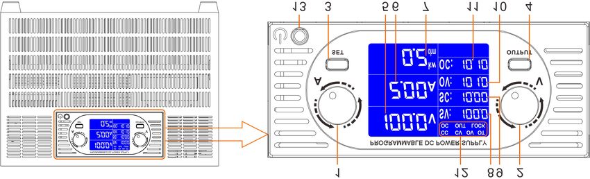
No. Name Description
1 Current knob Adjustment of the current limit value.
2 Voltage knob Adjustment of the voltage limit value.
3 SET button Switching between SETUP and DISPLAY modes.
4 OUTPUT button Enabling the output.
5 Voltmeter Displaying the real output voltage.
6 Ammeter Displaying the real output current.
7 Power / Resistance meter Displaying the real output power and resistance of the load.
8 Set Voltage display Displaying the set voltage value.
9 Set Current display Displaying the set current value.
10 Over voltage setting Displaying the set over voltage setting.
11 Over current setting Displaying the set over current value.
12 Status display Displaying the status of the power supply.
CC Constant current operation mode.
CV Constant voltage operation mode.
OV Over voltage protection triggered.
OT Over temperature protection triggered.
OC Over current protection triggered.
OUT Output enabled.
LOCK Panel locked.
13 Power switch Powering on the power supply.
DSC-Electronics Germany • Georgstraße 36 • 53111 Bonn
DSC-Electronics Germany • Georgstraße 36 • 53111 Bonn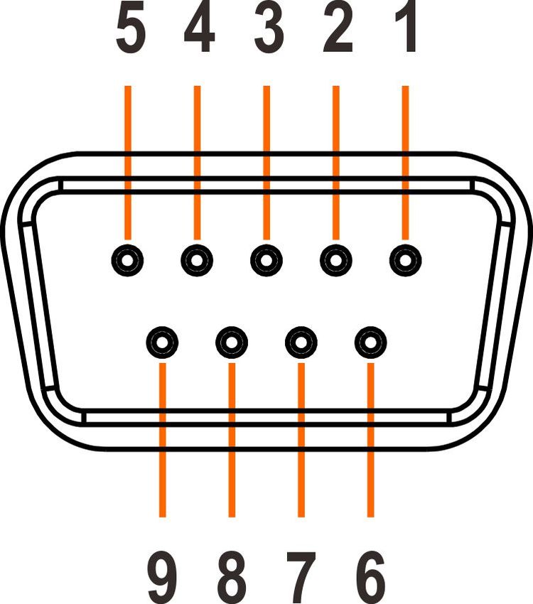
DP-D Gen2 Series User’s Manual
Version 25.02.2021

No.     Name                    Description
1       RS-232 Interface        Standard interface.
2       RS-485 Interface        Standard interface.
3       RS-485-Interface        Standard interface.
4       Analog control switch   Enable / Disable external analog control (Optional).
5       Output terminals        Positive and negative output terminals.
6       AC input terminals      AC mains connection.

4.2 DP-G Gen2 front and rear panel with option [Y]

No.    Name                     Description
1      Power switch             Power supply power ON/OFF.
2      Screen ON/OFF key        Press to enable or disable the front sceen. While the front screen is turned off, no
                                inputs over the front panel are possible (locked), remote control remains active.
3      Menu button              Press to enter system settings menu. Short press is again to select a sub-menu.
4      Tab key                  Cycle through tabs in the menu section.
5      Lock key                 Press to lock front panel and remote control to the currently set state. Inputs either
                                through the front panel, or remote control, will be discarded.
6      Store button             Save a screen shot of the curent display to the attached USB Stick.
7      USB Host port            Can handle USB sticks with FAT-32/16 and Ex-FAT format.
8      ← key                    Backspace.
9      Output ON/OFF key        Press to turn ON/OFF the output of the power supply.
10     < > keys                 Cursor keys. Press to move cursor to the left or right.
11     Rotary knob              Turn anti-clockwise to increase a value, or clockwise to decrease a value. After the
                                value is set, make a short press on the knob to save the setup and exit setup mode.
12     Numeric keypad           Input keys for numbers 1 to 9 and decimal point.
13     Function keys F1-F4      Press the key to select its corresponding parameter.
14     LCD display screen       -

                             DSC-Electronics Germany • Georgstraße 36 • 53111 Bonn
                             DSC-Electronics Germany • Georgstraße 36 • 53111 Bonn
DP-D Gen2 Series User’s Manual
Version 25.02.2021

No.     Name                     Description
1       RS-232 Interface         Standard interface.
2       RS-485 Interface         Standard interface.
3       RS-485-Interface         Standard interface.
4       Analog control switch    Enable / Disable external analog control (Optional).
5       Output terminals         Positive and negative output terminals.
6       AC input terminals       AC mains connection.

5. Operation instructions for devices without option [Y]
The DP-D Gen2 power supply can be optionally equipped with external analog control and feedback connections,
which allow to regulate and measure the set and real output values of the power supply externally. At the same time,
either external analog control or digital and the front panel controls can be used, thus make sure to select your desired
control method with the switch 4 on the rear panel before operation.

Caution: Always check that the output is switched off and the capacitors are discharged before connecting the load to
the power supply.

5.1 SET Button operation

1. Turn on the power and check that the output is off.
2. Press the SET button to enter SETTING mode.
3. Now adjust the output voltage and current with the voltage and current knobs.
4. Press the SET button once again to select the over voltage and over current settings.
5. Now adjust the over voltage and over current protection values.
6. Press the SET button once again to save all settings.
7. Turn on the output by pressing the OUTPUT button.

5.2 CV Constant voltage operation

NOTE: Pressing the voltage or current knob shortly switches between coarse and fine tuning.

1. Turn on the power and check that the output is off.
2. Press the SET button and set the desired voltage and current limit according to point 5.2.
4. Turn on the output by pressing the OUTPUT button.
5. The CV indicator lights up.
6. The power supply is now operating in constant voltage mode (CV).

The output voltage remains stable while the current is adjusted automatically. If the current exceeds the maximum
limit set, the power supply switches to CC mode and reduces the voltage not to exceed the maximum current limit.

                              DSC-Electronics Germany • Georgstraße 36 • 53111 Bonn
                              DSC-Electronics Germany • Georgstraße 36 • 53111 Bonn
DP-D Gen2 Series User’s Manual
Version 25.02.2021
5.3 Constant current operation
NOTE: Pressing the voltage or current knob shortly switches between coarse and fine tuning.
1. Turn on the power and check that the output is off.
2. Press the SET button and set the desired voltage and current limit according to point 5.2.
4. Turn the output on by pressing the OUTPUT button.
5. The CC indicator lights up as soon as the output current reaches the current limit set.
The power supply now operates in constant current mode (CC). The output current remains stable while the voltage is
being adjusted automatically.
5.4 Locking the front panel
Press the current knob for 3 seconds to lock or unlock the front panel. The current and voltage knob as well as the
SET button are not operational when the front panel is locked.
6. Operation instructions for devices with option [Y]
The DP-D Gen2 power supply can be optionally equipped with external analog control and feedback connections,
which allow to regulate and measure the set and real output values of the power supply externally. At the same time,
either external analog control or digital and the front panel controls can be used, thus make sure to select your desired
control method with the switch 4 on the rear panel before operation.
Caution: Always check that the output is switched off and the capacitors are discharged before connecting the load to
the power supply.
6.1 Set voltage
Press [F1] key to enter voltage setup mode (V-Set), now the cursor appears on voltage value position. The voltage
value can be set up in two ways:
- Adjust voltage value by rotary knob
- Input voltage value through the keypad
Press < > keys to move the cursor to the position that you would like to adjust, this also works with the rotary knob.
When the voltage value is adjusted to the desired value, short press the rotary knob to store the value and exit setup
mode.
6.2 Set current
Press [F2] key to enter current setup mode (I-Set), now the cursor appears on current value position. Perform the
current setup the same way as described in the voltage setup section above.
6.3 Set OVP
Press [F3] key to enter over voltage protection (OVP) limit setup mode (V-Limit). The cursor appears on voltage limit
value position. Perform the current setup the same way as described in the voltage setup section above.
6.4 Set OCP
Press [F4] key to enter over current protection (OCP) limit setup mode (I-Limit). The cursor appears on current limit
value position. Perform the current setup the same way as described in the voltage setup section above.
6.5 Set output On/Off
After power on, the power supply output status is defaulted to OFF. Output has to be turned on by pressing the on/off
key. Short press the [ON] key to turn on the output. The “ON” icon appears on the lower left corner of the LCD screen
when output is turned on. Short press the [ON] key again to turn off output. The “Off” icon appears on the lower left
corner of the LCD screen when the output is off.
DSC-Electronics Germany • Georgstraße 36 • 53111 Bonn
DSC-Electronics Germany • Georgstraße 36 • 53111 BonnDP-D Gen2 Series User’s Manual
Version 25.02.2021
6.6 Panel lock
The panel lock function is designed to avoid inputs by mistake.
Short press [Lock] key to lock operations of front panel keys and knobs. The “Lock” icon appears the lower left corner
of the LCD screen when the front panel is locked. Inputs of all keys and knobs are invalid, except operation of the [ON]
key. If output is on during panel lock, the [ON] key can be pressed to turn off the output. However, output cannot be
turned on again by pressing the [ON] key while the panel is locked. The front panel can be unlocked by pressing the
[Lock] key again.
6.7 System setup
Press the [Menu] button for two times to select “System Setup” mode.
6.7.1 Set output mode
There are four output modes to be chosen from. Press the [Tab] button to select the “MODE” menu. Use the rotary
knob to select an output mode from the “Mode Select” setting.
Normal mode: In this mode, output voltage and current is set up by manual configuration on front panel or through
external interfaces.
Cycle mode: In this mode, maximum 999999 steps can be set into one automatic running cycle. Output voltage,
current and time can be set up in each step.
V Slope mode: In this mode, voltage rise/fall time can be adjusted.
I-Slope mode: In this mode, current rise/fall time can be adjusted.
Depending on the mode chosen, the sixth tab in the main menu gets replaced by the appropriate configuration utility
for the mode chosen.
DSC-Electronics Germany • Georgstraße 36 • 53111 Bonn
DSC-Electronics Germany • Georgstraße 36 • 53111 BonnDP-D Gen2 Series User’s Manual
Version 25.02.2021
6.7.2 Serial communication
Press the [Tab] button to select the “UART” menu. In this menu, parameters of baud rate, stop bit, parity bit and
communication ID can be adjusted. Press < > keys to move the cursor to select a parameter, and then use the rotary
knob to set the value. Communication ID defaults to 0.
6.7.3 LAN Communication
Press the [Tab] button to select the “LAN” menu. LAN communication settings include automatic IP address
allocation “DHCP” and fixed IP address settings “Fixed IP”, as well as subnet mask settings “NM” and default gateway
settings “GW”. Also the currently assigned IP address and communication protocol is displayed. The host port number
defaults to 502.
DSC-Electronics Germany • Georgstraße 36 • 53111 Bonn
DSC-Electronics Germany • Georgstraße 36 • 53111 BonnDP-D Gen2 Series User’s Manual
Version 25.02.2021
6.7.4 Date and time
Press the [Tab] button to select the “DATE & TIME” menu. Press the < > keys to move cursor to select a parameter,
and then use rotary knob to set the value.
6.7.5 Protection settings
Press the [Tab] button to select the “PROTECT” menu. The over voltage protection and over current protection
functions can be turned on and off depending on the settings here. Press the < > keys to move the cursor to select a
protection mode, and then use the rotary knob to switch between on and off.
DSC-Electronics Germany • Georgstraße 36 • 53111 Bonn
DSC-Electronics Germany • Georgstraße 36 • 53111 BonnDP-D Gen2 Series User’s Manual
Version 25.02.2021
6.7.6 Cycle mode settings
Press the [Tab] button to select the “CYCLE MODE” menu.
There are 4 cycle configuration options:
10 group * 100 item (100 steps in each group, in total 10 groups)
20 group * 50 item (50 steps in each group, in total 20 groups)
50 group * 20 item (20 steps in each group, in total 50 groups)
100 group * 10 item (10 steps in each group, in total 100 groups)
Press the < > keys to move the cursor and select a cycle configuration.
Press the < > keys or turn the rotary knob to move the cursor to the row entitled as “Group:, StartStep:, EndStep:”, the
cursor position is highlighted in blue as above.
Function keys F1-F4 now correspond to Group No. [Group], Start Step No. [StartStep], End Step No. [EndStep] and
[BackSpace] key respectively. Press F1-F4 keys to select a parameter. Input a new parameter via keypad or rotary
knob, and make a short press on the rotary knob to confirm input.
DSC-Electronics Germany • Georgstraße 36 • 53111 Bonn
DSC-Electronics Germany • Georgstraße 36 • 53111 BonnDP-D Gen2 Series User’s Manual
Version 25.02.2021
Press the < > keys or turn the rotary knob to move the cursor to the row entitled as “Cycle:, OVP:, OCP:”, the cursor
position is highlighted in blue as above.
Function keys F1-F4 now correspond to Cycle No. [Cycle], OVP value [OVP], OCP value [OCP] and [BackSpace] key
respectively. Press F1-F4 keys to select a parameter. Input a new parameter via keypad or rotary knob, and make a
short press on the rotary knob to confirm input.
Press the < > keys or turn the rotary knob to move the cursor to the first row of the table, the cursor position is
highlighted in blue as above.
Function keys F1-F4 now correspond to Step No. [Step], Voltage value [V (V)], Current value [I(A)], time value [Hr Min
Sec] and [BackSpace] key respectively. Press F1-F4 keys to select a parameter. Input a new parameter via keypad or
rotary knob, and make a short press on the rotary knob to confirm input.
DSC-Electronics Germany • Georgstraße 36 • 53111 Bonn
DSC-Electronics Germany • Georgstraße 36 • 53111 BonnDP-D Gen2 Series User’s Manual
Version 25.02.2021
6.7.7 V Slope mode
In voltage slope mode, the output voltage rise time or fall time can be adjusted. After setting up rise time or fall time,
the output voltage rises or falls gradually within the preset time. Otherwise, the output voltage rises or falls at the
maximum speed. The rise or fall time can be adjusted to max 99999 seconds.
Press the < > keys or turn the rotary knob to move the cursor to the row entitled as “Group:, StartStep:, EndStep:”, the
cursor position is highlighted in blue as above.
Function keys F1-F4 now correspond to Group No. [Group], Cycle No. [Cycle], Start Step No. [StartStep], End Step No.
[EndStep] and [BackSpace] key respectively. Press F1-F4 keys to select a parameter. Input a new parameter via
keypad or rotary knob, and make a short press on the rotary knob to confirm input.
Press the < > keys or turn the rotary knob to move the cursor to the row entitled as “Iset:, OVP:, OCP:”, the cursor
position is highlighted in blue as above.
Function keys F1-F4 now correspond to OVP value [OVP], OCP value [OCP] and [BackSpace] key respectively. Press
F1~F4 keys to select a parameter. Input a new parameter via keypad or rotary knob, and make a short press on the
rotary knob to confirm input.
DSC-Electronics Germany • Georgstraße 36 • 53111 Bonn
DSC-Electronics Germany • Georgstraße 36 • 53111 BonnDP-D Gen2 Series User’s Manual
Version 25.02.2021
Press the < > keys or turn the rotary knob to move the cursor to the first row of the table, the cursor position is
highlighted in blue as above.
Function keys F1-F4 now correspond to Step No. [Step], Voltage value [V(V)], Current value [I(A)], time value [Hr Min
Sec] and [BackSpace] key respectively. Press F1-F4 keys to select a parameter. Input a new parameter via keypad or
rotary knob, and make a short press on the rotary knob to confirm input.
6.7.8 Other settings
Beeper: Beeper alarm can be turn on and off.
Volume: Beeper volume can be set from low to high in 6 steps. Volume defaults to lowest range 1.
Startup Output on: The output defaults to off after startup, but can be set to on.
Backlight: The brightness of the LCD backlight can be set from low to high in 8 steps. Brightness defaults to the
lowest step 1.
Upgrade: Begin firmware upgrade from an external USB stick.
Keep only one (the latest) BIN file on the USB flash drive that is used for firmware upgrade. If there is more than a
single firmware file, the system cannot identify which file to use for this particular upgrade.
Plug in the USB flash drive with the .bin firmware file after startup and select “Upgrade” in the “OTHER” tab. To avoid
accidential firmware modifications, you will have to confirm the firmware upgrade by turning the rotary knob to
increase the counter to “5/5”. The power supply will start to read the BIN file and begin automatic upgrade. Please
under no circumstances power off the power supply during the upgrade.
Factory setting: Resets the power supply configuration to factory settings.
DSC-Electronics Germany • Georgstraße 36 • 53111 Bonn
DSC-Electronics Germany • Georgstraße 36 • 53111 BonnDP-D Gen2 Series User’s Manual
Version 25.02.2021
7. Optional features
7.1 Remote sensing
The power supply is optionally equipped with remote sensing terminals, which can read the voltage at the load and
therefore compensate losses. Refer to below figure on how to connect the load to remote sensing terminals. The
remote sensing input can be connected optionally, and is automatically deactivated if not connected.
WARNING: In case you physically disconnect the output leads from the load, also disconnect the remote sensing
leads at the same time.
7.2 External „Output ON/OFF“ Control & Interlock
Input for controlling the status of the output of the laboratory power supply (on / off), switchable as “Interlock” or
external control. This input is configured as a two pin connection, a „true“ state is triggered by shorting the two pins
and a „false“ state is triggered by removing any connection between the two pins of the input.
This option can be configured as either an interlock input, which disables the output of the power supply if the state is
false, or as an external output status control which enables or disables the output of the power supply depending on
the control signal state (true = on/false = off) if the „Output On/Off“ switch of the power supply is always in the ON
position.
8. Digital control
8.1 RS-232 Interface
Following the pin description of the RS-232 interface of the DP-D Gen2 Series.
Pin Pin out definition Function
1 NC Blank
2 TXD Send
3 RXD Receive
4 NC Blank
5 GND Ground
6 NC Blank
7 NC Blank
8 NC Blank
9 NC Blank
DSC-Electronics Germany • Georgstraße 36 • 53111 Bonn
DSC-Electronics Germany • Georgstraße 36 • 53111 BonnDP-D Gen2 Series User’s Manual
Version 25.02.2021
8.2 RS-485 Interface
Following the pin description of the RS-485 interface of the DP-D Gen2 Series.
Pin Pin out definition Function
1 A (D+) -
2 B (D-) -
3 NC -
4 NC -
5 NC -
6 NC -
7 NC -
8 NC -
Space for your notes:
DSC-Electronics Germany • Georgstraße 36 • 53111 Bonn
DSC-Electronics Germany • Georgstraße 36 • 53111 BonnDP-D Gen2 Series User’s Manual
Version 25.02.2021
9. Communication Protocol for DSC-Electronics DP-D Gen2 Series power supplies
Interface: RS-232 / RS-485 (Profibus DB) / LAN (Only with option[Y])
Command format: Asynchronous, 1 start bit, 8 data bits, 1 stop bit
UART baud rate: 1200; 2400; 4800; (9600 default); 14400; 19200; 38400; 43000; 57600; 76800; 115200; 128000
Communicationmode: Master-Slave mode
Command Format
1st part: ID number of the DC power supply, 1-16 (If the ID number is 0, all devices will respond)
2nd part: Control command
3rd part: Data length (how many values are supplied to the device in this command)
Data part: 16-bit data, high bit in the front
CRC part: MODBUS format, low byte in the front
Feedback Command Format
1st part: ID number of the DC power supply, 1-16
2nd part: control command
3rd part: data length (how many values are supplied to the device in this command)
Data part: 16-bit data, high bit in the front
CRC check: MODBUS format, low byte in the front
The power supply automatically switches to remote operation mode as soon as contacted through one of the digital
interfaces. The below information is displayed while the device is in remote operation mode (not on devices with the
[Y] option).
DSC-Electronics Germany • Georgstraße 36 • 53111 Bonn
DSC-Electronics Germany • Georgstraße 36 • 53111 BonnDP-D Gen2 Series User’s Manual
Version 25.02.2021
9.1 Command Examples
9.1.1 Output ON/OFF
Control command:
ID Function Code Register Address Data (On/Off) CRC Check Code
01 05 0085 FF00 9DD3
01 05 0085 0000 DC23
Feedback: Equal to command.
9.1.2 Read Output Status
Control command:
ID Function Code Address of Start Register Numbers of Registers CRC Check Code
01 01 0085 0001 EC23
Feedback:
ID Function Code Address of First Register Output Status (On/Off) CRC Check Code
01 01 01 01 9048
01 01 01 00 5188
9.1.3 Read Output Voltage Value
Control command:
ID Function Code Address of First Register Numbers of Registers CRC Check Code
01 04 0064 0001 7015
Feedback:
ID Function Code Bytes Output Voltage CRC Check Code
01 04 02 0283 F9F1
Voltage: 0x0283 in decimal equals to 643.
643 divided by 10 (1 decimal point) is 64.3, thus a voltage value of 64.3V.
9.1.4 Read Output Voltage and Current Value
Control command:
ID Function Code Address of First Register Numbers of Registers CRC Check Code
01 04 0064 0002 7015
Feedback:
ID Function Code Bytes Output Voltage Output Current CRC Check Code
01 04 02 0283 0001 CA14
Voltage: 0x0001 in decimal equals to 1.
1 divided by 100 is (2 decimal points) 0.01, thus a current value of 0.01A.
9.1.5 Read Output Power Value
Control command:
Register Type Function Address Address (Hex) Target Function Code 04
(Decimal) (Read)
3 Read Output power 102 0x0066 Byte √
(feedback value)
This is an optional command and is not available in standard configurations.
Below commands are used to read output power value in standard configuration devices.
Register Type Function Address Address (Hex) Target Function Code 04
(Decimal) (Read)
11 Read Output power KW*1 110 0x006E Byte √
12 Read Output power W*1 111 0x006F Byte √
13 Read Output power 112 0x0070 Byte √
mW*1
DSC-Electronics Germany • Georgstraße 36 • 53111 Bonn
DSC-Electronics Germany • Georgstraße 36 • 53111 BonnDP-D Gen2 Series User’s Manual
Version 25.02.2021
Control command:
ID Function Code Address of First Register Numbers of Registers CRC Check Code
01 04 006E 0003 DID6
Feedback:
ID Function Code Bytes KW W mW CRC Check Code
01 04 06 0000 007F 02E8 F9F1
KW: 0x0000 = 0kW
W: 0x007F = 127W
Mw: 0x02E8 = 744mW
Output power: 0+127+0.744 = 127.744W
The power value is calculated from the voltage and current readback value, so the digits of the read power value may
be two decimal points longer than the digits displayed by the power supply.
9.1.6 Read Rated Voltage Value
Control command:
ID Function Code Address of First Register Numbers of Registers CRC Check Code
01 04 0067 0001 8015
Feedback:
ID Function Code Bytes Output Voltage CRC Check Code
01 04 02 03E8 B98E
Voltage: 0x03E8 into decimal system is 1000.
1000 divided by 10 is (1 decimal point) 100.0, thus the voltage value is 100.0V.
9.1.7 Set Output Voltage Value
Control command:
ID Function Code Register Address Data CRC Check Code
01 06 0095 01F4 99F1
Feedback:
ID Function Code Register Address Data CRC Check Code
01 06 0095 01F4 99F1
Set output voltage to 50V. There is 1 decimal point for voltage value (50.0).The value should be 500 in the decimal
system. 500 into hex is 0x01F4.
9.1.8 Set Output Voltage and Current Value
Control command:
ID Function Code Address of Numbers of Bytes Voltage Current CRC Check Code
First Register Registers
01 10 0095 0002 04 0190 01F4 3B3A
Feedback:
ID Function Code Address of First Register Numbers of Registers CRC Check Code
01 10 0095 0002 51E4
9.1.9 Set Cycle Mode
1) Change Operation Mode of the Power Supply
Control command:
ID Function Code Register Address Data CRC Check Code
01 06 00A0 0000 (Normal mode) 89E8
01 06 00A0 0001 (Cycle mode) 4828
Feedback: Equal to command.
DSC-Electronics Germany • Georgstraße 36 • 53111 Bonn
DSC-Electronics Germany • Georgstraße 36 • 53111 BonnDP-D Gen2 Series User’s Manual
Version 25.02.2021
2) Set Voltage Value of Sequence Number 1 to X
For example, set voltage values of sequence number 1, 2 and 3 at 2.4V, 3.4V and 5.4V respectively.
ID Function Code Address of Numbers of Bytes #1 #2 #3 CRC Check Code
First Register Registers
01 10 03E9 0003 06 0018 0022 0036 3DA3
Feedback data:
ID Function Code Address of First Register Numbers of Registers CRC Check Code
01 10 03E9 0003 51B8
3) Set Current Value of Sequence Number 1 to X
For example, set current values of sequence number 1, 2 and 3 at 10.00A.
ID Function Code Address of Numbers of Bytes #1 #2 #3 CRC Check Code
First Register Registers
01 10 044D 0003 06 03E8 03E8 03E8 8074
Feedback:
ID Function Code Address of First Register Numbers of Registers CRC Check Code
01 10 044D 0003 112F
4) Set Running Time Value of Sequence Number 1 to X
For example, set running time values of sequence number 1, 2 and 3 at 15s, 10s, and 5s respectively.
ID Function Code Address of Numbers of Bytes #1 #2 #3 CRC Check Code
First Register Registers
01 10 04B1 0003 06 000F 000A 0005 1162
Feedback:
ID Function Code Start Address of Register Numbers of Registers CRC Check Code
Address
01 10 04B1 0003 D11F
9.1.10 Set Cycle Numbers
Control command:
ID Function Code Register Address Data CRC Check Code
01 06 00A4 0004 082A
Feedback: Equal to command.
Remarks:
1) While the output is ON, the power supply operating mode cannot be changed, nor can the voltage, current, or time
values be changed.
2) In cycle mode, the voltage, current, and time under each sequence number must be set. If the voltage and current
are set to 0, the power output is 0. If the time is set to 0, this sequence number is not run.
Space for your notes:
DSC-Electronics Germany • Georgstraße 36 • 53111 Bonn
DSC-Electronics Germany • Georgstraße 36 • 53111 BonnDP-D Gen2 Series User’s Manual
Version 25.02.2021
9.2 Command Frame
9.2.1 Function Code
Below function codes are supported.
Function Function Description Bit Operation / Numbers of Operation
Code Code HEX Byte Operation
01 0x01 Read cycle status Bit Operation Single or multiple
02 0x02 Read discrete input status Bit Operation Single or multiple
03 0x03 Read holding register Byte Operation Single or multiple
04 0x04 Read input register Byte Operation Single or multiple
05 0x05 Write single cycle Bit Operation Single
06 0x06 Write single holding register Byte Operation Single
15 0x0f Write multiple cycles Bit Operation Multiple
16 0x10 Write Multiple holding register Byte Operation Multiple
Bit operation: Read/write cycle, read/write data bit by bit.
Byte Operation: Read/write register, read/write data byte by byte.
Space for your notes:
DSC-Electronics Germany • Georgstraße 36 • 53111 Bonn
DSC-Electronics Germany • Georgstraße 36 • 53111 BonnDP-D Gen2 Series User’s Manual
Version 25.02.2021
9.2.2 Register Definition
Input Register
Address Address Function Code
No Type Description Target
(Decimal) (Hex) 04 (Read)
1 Read Output voltage (feedback value) 100 0x0064 Byte √
2 Read Output current (feedback value) 101 0x0065 Byte √
3 Read Output power (feedback value) 102 0x0066 Byte √
4 Read Rated voltage 103 0x0067 Byte √
5 Read Rated current 104 0x0068 Byte √
6 Read Reserved 105 0x0069
7 Read Voltage decimal point 106 0x006a Byte √
8 Read Current decimal point 107 0x006b Byte √
9 Read Reserved 108 0x006c
10 Read Reserved 109 0x006d
11 Read Output power-KW*1 110 0x006e Byte √
12 Read Output power-W*1 111 0x006f Byte √
13 Read Output power-mW*1 112 0x0070 Byte √
14 Read Load resistance-Kohm*1 113 0x0071 Byte √
15 Read Load resistance-ohm*1 114 0x0072 Byte √
16 Read Load resistance-mohm*1 115 0x0073 Byte √
17 Read Reserved 116 0x0074 Byte √
18 Read Reserved 117 0x0075 Byte √
19 Read Reserved 118 0x0076 Byte √
20 Read Reserved 119 0x0077 Byte √
21 Read Reserved 120 0x0078 Byte √
22 Read Reserved 121 0x0079 Byte √
23 Read Reserved 122 0x007a Byte √
24 Read Reserved 123 0x007b Byte √
25 Read The running sequence number in cycle
124 0x007c Byte √
mode
26 Read The run cycle numbers in cycle mode 125 0x007d Byte √
27 Read The running time in cycle model (hour) 126 0x007e Byte √
28 Read The running time in cycle model (minute) 127 0x007f Byte √
29 Read The running time in cycle model (second) 128 0x0080 Byte √
30 Read Total number of cycles in cycle mode 129 0x0081 Byte √
31 Read Total numbers of sequences in each cycle 130 0x0082 Byte √
32 Read Reserved 131 0x0083 Byte √
33 Read Reserved 132 0x0084 Byte √
34 Read Reserved 133 0x0085 Byte √
35 Read Reserved 134 0x0086 Byte √
36 Read Reserved 135 0x0087 Byte √
37 Read Reserved 136 0x0088 Byte √
38 Read Reserved 137 0x0089 Byte √
39 Read Reserved 138 0x008a Byte √
40 Read Reserved 139 0x008b Byte √
41 Read Reserved 140 0x008c Byte √
42 Read Reserved 141 0x008d Byte √
DSC-Electronics Germany • Georgstraße 36 • 53111 Bonn
DSC-Electronics Germany • Georgstraße 36 • 53111 BonnDP-D Gen2 Series User’s Manual
Version 25.02.2021
Discrete Input Status
Address Address Function Code
No Type Description Target
(Decimal) (Hex) 02 (Read)
1 Read Constant Current mode (CC) 116 0x0074 Bit √
2 Read Constant Voltage mode (CV) 117 0x0075 Bit √
3 Read Reserved 118 0x0076
4 Read Reserved 119 0x0077
5 Read Over Voltage Protection (OVP) 120 0x0078 Bit √
6 Read Over Current Protection (OCP) 121 0x0079 Bit √
7 Read Over Temperature Operation (OTP) 122 0x007a Bit √
8 Read Reserved 123 0x007b
9 Read Reserved 124 0x007c
10 Read Reserved 125 0x007d
11 Read Reserved 126 0x007e Bit √
Cycle
Function Code
Address Address 01 05 15
No Type Description Target
(Decimal) (Hex) (Read) (Write (Write
single) multiple)
1 R/W Reserved 132 0x0084
2 R/W Output switch 133 0x0085 Bit √ √ √
3 R/W Lock 134 0x0086 Bit √ √ √
4 R/W Reserved 135 0x0087
5 R/W OVP allowed 136 0x0088 Bit √ √ √
6 R/W OCP allowed 137 0x0089 Bit √ √ √
7 R/W Reserved 138 0x008a
8 R/W Reserved 139 0x008b
9 R/W Reserved 140 0x008c
10 R/W Reserved 141 0x008d
11 R/W Save output status 142 0x008e Bit √ √ √
12 R/W Reserved 143 0x008f Bit √ √ √
Space for your Notes:
DSC-Electronics Germany • Georgstraße 36 • 53111 Bonn
DSC-Electronics Germany • Georgstraße 36 • 53111 BonnDP-D Gen2 Series User’s Manual
Version 25.02.2021
Holding Register
Function Code
Address Address 03 06 16
No Type Description Target
(Decimal) (Hex) (Read) (Write (Write
single) multiple)
1 R/W ID 148 0x0094 Byte √ √ √
2 R/W Voltage setup value 149 0x0095 Byte √ √ √
3 R/W Current setup value 150 0x0096 Byte √ √ √
4 R/W Power setup value (optional) 151 0x0097 Byte √ √ √
5 R/W Line resistance (optional) 152 0x0098 Byte √ √ √
6 R/W Low bit of PWM frequency
153 0x0099 Byte √ √ √
(optional)
7 R/W High bit of PWM frequency
154 0x009a Byte √ √ √
(optional)
8 R/W PWM duty cycle (optional) 155 0x009b Byte √ √ √
9 R/W Baud rate*2 156 0x009c Byte √ √ √
10 R/W OVP value 157 0x009d Byte √ √ √
11 R/W OCP value 158 0x009e Byte √ √ √
12 R/W OPP value (optional) 159 0x009f
13 R/W Operation mode*3 160 0x00a0 Byte √ √ √
14 R/W Running cycle number in cycle
161 0x00a1 Byte √ √ √
mode
15 R/W The 1st sequence number in
162 0x00a2 Byte √ √ √
cycle mode
16 R/W The last sequence number in
163 0x00a3 Byte √ √ √
cycle mode
17 R/W Total number of cycles in cycle
164 0x00a4 Byte √ √ √
mode
18 R/W Reserved 165 0x00a5 Byte √ √ √
19 R/W Reserved 166 0x00a6 Byte √ √ √
20 R/W Reserved 167 0x00a7 Byte √ √ √
21 R/W Reserved 168 0x00a8 Byte √ √ √
22 R/W Running cycle number of V-Slope
169 0x00a9 Byte √ √ √
mode.
23 R/W Current setup value in V-Slope
170 0x00aa Byte √ √ √
mode
24 R/W Start step in V Slope mode 171 0x00ab Byte √ √ √
25 R/W End step in V Slope mode 172 0x00ac Byte √ √ √
26 R/W Cycle numbers in V-Slope mode 173 0x00ad Byte √ √ √
27 R/W Reserved 174 0x00ae Byte √ √ √
28 R/W Reserved 175 0x00af Byte √ √ √
29 R/W Reserved 176 0x00b0 Byte √ √ √
30 R/W Reserved 177 0x00b1 Byte √ √ √
31 R/W Running cycle number of I-Slope
Byte √ √ √
mode. 178 0x00b2
32 R/W Voltage setup in I-Slope mode 179 0x00b3 Byte √ √ √
DSC-Electronics Germany • Georgstraße 36 • 53111 Bonn
DSC-Electronics Germany • Georgstraße 36 • 53111 BonnDP-D Gen2 Series User’s Manual
Version 25.02.2021
Holding Register
Function Code
Address Address 03 06 16
No Type Description Target
(Decimal) (Hex) (Read) (Write (Write
single) multiple)
33 R/W Start step in I-Slope mode 180 0x00b4 Byte √ √ √
34 R/W End step in I-Slope mode 181 0x00b5 Byte √ √ √
35 R/W Cycle numbers in I-Slope mode 182 0x00b6 Byte √ √ √
36 R/W Reserved 183 0x00b7 Byte √ √ √
37 R/W Reserved 184 0x00b8 Byte √ √ √
38 R/W Reserved 185 0x00b9 Byte √ √ √
39 R/W Reserved 186 0x00ba Byte √ √ √
40 R/W Year 187 0x00bb Byte √ √ √
41 R/W Month 188 0x00bc Byte √ √ √
42 R/W Date 189 0x00bd Byte √ √ √
43 R/W Time 190 0x00be Byte √ √ √
44 R/W Minute 191 0x00bf Byte √ √ √
45 R/W Second 192 0x00c0 Byte √ √ √
46 R/W LAN DHCP switch (optional) 193 0x00c1 Byte √ √ √
47 R/W LAN IP part1 (optional) 194 0x00c2 Byte √ √ √
48 R/W LAN IP part2 (optional) 195 0x00c3 Byte √ √ √
49 R/W LAN IP part3 (optional) 196 0x00c4 Byte √ √ √
50 R/W LAN IP part4 (optional) 197 0x00c5 Byte √ √ √
51 R/W LAN subnet mask part1 (optional) 198 0x00c6 Byte √ √ √
52 R/W LAN subnet mask part2 (optional) 199 0x00c7 Byte √ √ √
53 R/W LAN subnet mask part3 (optional) 200 0x00c8 Byte √ √ √
54 R/W LAN subnet mask part4 (optional) 201 0x00c9 Byte √ √ √
55 R/W LAN default gateway part1 202 0x00ca Byte √ √ √
56 R/W LAN default gateway part2 203 0x00cb Byte √ √ √
57 R/W LAN default gateway part3 204 0x00cc Byte √ √ √
58 R/W LAN default gateway part4 205 0x00cd Byte √ √ √
59 R/W Voltage of sequence 1 in Cycle 1001 0x03e9
Byte √ √ √
Mode
60 R/W Voltage of sequence X in Cycle
1000+X Byte √ √ √
Mode
61 R/W Voltage of sequence 100 in Cycle 1100 0x044c
Byte √ √ √
Mode
62 R/W Current of sequence 1 in Cycle 1101 0x044d
Byte √ √ √
Mode
63 R/W Current of sequence X in Cycle
1100+X Byte √ √ √
Mode
64 R/W Current of sequence 100 in Cycle 1200 0x04b0
Byte √ √ √
Mode
65 R/W Running time of sequence 1 in 1201 0X04B1
Byte √ √ √
Cycle Mode
DSC-Electronics Germany • Georgstraße 36 • 53111 Bonn
DSC-Electronics Germany • Georgstraße 36 • 53111 BonnDP-D Gen2 Series User’s Manual
Version 25.02.2021
Holding Register
Function Code
Address Address 03 06 16
No Type Description Target
(Decimal) (Hex) (Read) (Write (Write
single) multiple)
66 R/W Running time of sequence X in
1200+X Byte √ √ √
Cycle Mode
67 R/W Running time of sequence 100 in 1300 0X0514
Byte √ √ √
Cycle Mode
68 R/W Start voltage of step 1 in V-Slope 1301 0x0515
Byte √ √ √
Mode
69 R/W End voltage of step 1 in V-Slope 1302 0x0516
Byte √ √ √
Mode
70 R/W End voltage of step X in V-Slope
1301+X Byte √ √ √
Mode
71 R/W End voltage of step 50 in V-Slope 1351 0x0547
Byte √ √ √
Mode
72 R/W Running time of step 1 in V-Slope 1401 0x0579
Byte √ √ √
Mode
73 R/W Running time of step X in Voltage
1400+X Byte √ √ √
Slope Mode
74 R/W Running time of step 50 in V- 1450 0x05aa
Byte √ √ √
Slope Mode
75 R/W Start current of step 1 in I-Slope 1501 0x05dd
Byte √ √ √
Mode
76 R/W End current of step 1 in I- Slope 1502 0x05de
Byte √ √ √
Mode
77 R/W End current of step X in I- Slope
1501+X Byte √ √ √
Mode
78 R/W End current of step 50 in I-Slope 1551 0x060f
Byte √ √ √
Mode
79 R/W Running time of step 1 in I-Slope 1601 0x0641
Byte √ √ √
Mode
80 R/W Running time of step X in I-Slope
1600+X Byte √ √ √
Mode
81 R/W Running time of step 50 in I- 1650 0x0672
Byte √ √ √
Slope Mode
Space for your notes:
DSC-Electronics Germany • Georgstraße 36 • 53111 Bonn
DSC-Electronics Germany • Georgstraße 36 • 53111 BonnDP-D Gen2 Series User’s Manual
Version 25.02.2021
Note: Registers marked yellow are only available on devices with option [Y].
Remark 1:
The output power and load resistance are calculated from the voltage and current readback values.
To get the present output power, you need to read the data of three addresses of kilowatts (KW), watts (W), and
milliwatts (mW) at one time. Set the three address data to A, B, and C. The output power value follows the following
formula:
Apply the same method to calculate load resistance value.
Remark 2:
Supported baud rates: 1200; 2400; 4800; 9600; 14400; 19200; 38400; 43000; 57600; 76800; 115200; 128000
Due to the limitation of single register data range (0~65535), the baud rate needs to be divided by 10, that is, remove a
0 at the end and write it.
Remark 3:
Operation Mode
Register Value Operation Mode
0 Normal mode
1 Cycle mode
10. Device Check
NOTE: The device check should only be performed for troubleshooting purposes.
1. Make sure that the device is correctly connected to the power grid.
2. Please do not connect any loads to the power supply during self-test.
3. Turn on the power, set the preset current to the highest possible value and the voltage to 0V.
4. Set the over current and over voltage protection limits to their maximum values.
5. Turn on the output and check the output voltage to be equal to the maximum voltage of the power supply model.
The power supply should be working in CV mode now.
6. Turn off the output, wait till the capacitors are discharged and the output voltage reaches 0V.
7. Set the preset current to 0A and leave the voltage at the maximum value.
8. Shorten the output terminals of the power supply with an appropriate cable or copper bar, which is able to
withstand the maximum current of the power supply for at least 30 seconds.
9. Turn on the output, slowly turn the output current up until you reach the maximum possible value. Check whether
the output current is equal to the maximum current of the power supply.
10.Turn off the output, turn off the power supply, disconnect the cable from the output terminals.
DSC-Electronics Germany • Georgstraße 36 • 53111 Bonn
DSC-Electronics Germany • Georgstraße 36 • 53111 BonnYou can also read