Dopant activity for highly in-situ doped polycrystalline silicon: hall, XRD, scanning capacitance microscopy (SCM) and scanning spreading ...
←
→
Page content transcription
If your browser does not render page correctly, please read the page content below

Nano Express

PAPER • OPEN ACCESS

Dopant activity for highly in-situ doped polycrystalline silicon: hall, XRD,
scanning capacitance microscopy (SCM) and scanning spreading
resistance microscopy (SSRM)
To cite this article: Rosine Coq Germanicus et al 2021 Nano Ex. 2 010037

View the article online for updates and enhancements.

                              This content was downloaded from IP address 46.4.80.155 on 12/09/2021 at 14:55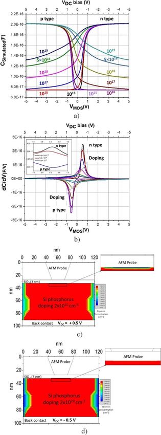
Nano Express 2 (2021) 010037                                                         https://doi.org/10.1088/2632-959X/abed3e

                              PAPER

                              Dopant activity for highly in-situ doped polycrystalline silicon: hall,
OPEN ACCESS
                              XRD, scanning capacitance microscopy (SCM) and scanning
RECEIVED
22 December 2020              spreading resistance microscopy (SSRM)
REVISED
2 March 2021
                              Rosine Coq Germanicus1 , Florent Lallemand2, Daniel Chateigner1 , Wadia Jouha3 , Niemat Moultif3,
ACCEPTED FOR PUBLICATION
9 March 2021
                              Olivier Latry3 , Arnaud Fouchet1, Hugues Murray1, Catherine Bunel2 and Ulrike Lüders1
                              1
                                  Normandie Univ, Ensicaen, Unicaen, Cnrs, Crismat, UMR 6508, 14000 Caen, France
PUBLISHED
                              2
18 March 2021                     Murata Integrated Passive Solutions, 2 Rue De La Girafe, 14000 Caen, France
                              3
                                  Normandie Univ, Groupe De Physique Des Materiaux (GPM), UMR 6634, Cnrs, 76000 Rouen, France

Original content from this    E-mail: rosine.germanicus@unicaen.fr
work may be used under
the terms of the Creative     Keywords: dopant activation, afm, scm, ssrm, polysilicon, passivating contact
Commons Attribution 4.0
licence.
Any further distribution of
this work must maintain       Abstract
attribution to the
author(s) and the title of
                              Progressing miniaturization and the development of semiconductor integrated devices ask for
the work, journal citation    advanced characterizations of the different device components with ever-increasing accuracy.
and DOI.
                              Particularly in highly doped layers, a fine control of local conduction is essential to minimize access
                              resistances and optimize integrated devices. For this, electrical Atomic Force Microscopy (AFM) are
                              useful tools to examine the local properties at nanometric scale, for the fundamental understanding of
                              the layer conductivity, process optimization during the device fabrication and reliability issues. By
                              using Scanning Capacitance Microscopy (SCM) and Scanning Spreading Resistance Microscopy
                              (SSRM), we investigate a highly in situ doped polycrystalline silicon layer, a material where the
                              electrical transport properties are well known. This film is deposited on a oxide layer as a passivating
                              contact. The study of the nano-MIS (SCM) and nano-Schottky (SSRM) contacts allows to determine
                              the distribution and homogeneity of the carrier concentration (active dopants), especially by
                              investigating the redistribution of the dopants after an annealing step used for their activation. While
                              the chemical analysis by Secondary Ions Mass Spectroscopy (SIMS) quantifies only the dopant
                              concentration in the polycrystalline layer, the comparison with macroscopic characterization
                              techniques as Hall effect measurements, supported with XRD characterization, shows that careful
                              SCM and SSRM measurements can be used to highlight the dopant activation. This analysis gives a
                              complete investigation of the local electrical properties of the passivating contact when the parameters
                              (applied voltages and applied forces) of the AFM nano-contacts are correctly controlled.

                              1. Introduction

                              Scanning Probe Microscopies (SPM) are powerful tools in the field of material characterizations at the nanoscale
                              [1, 2]. Since its invention, over 30 years ago, several electrical modes have been developed and optimized based
                              on Atomic Force Microscopy (AFM) [3–5]. For microelectronic characterization at the wafer level, both
                              Scanning Capacitance Microscopy (SCM) [6–8] and Scanning Spreading Resistance Microscopy (SSRM) [9, 10]
                              modes have been implemented to map carrier concentrations of semiconductors with high spatial resolution
                              [5, 9, 11]. These two electrical modes are contact modes, where conductive tips interact with the sample to probe
                              the local electrical properties [12, 13]. Figure 1 presents the Scanning Electron Microscopy (SEM) views of the
                              used probes. The size of the contact dependents directly on the tip apex and the surface roughness of the
                              analyzed sample. The SCM probe (figure 1(a)) is a silicon probe fabricated for contact the analyzed surface (with
                              this cantilever a relative low force is applied). The diamond coating of the SSRM probe (figure 1(b)) allows to
                              increase the tip conductivity and the spring-constant of the cantilever, in order to indent the surface and create
                              the electrical path through the sample.

                              © 2021 The Author(s). Published by IOP Publishing Ltd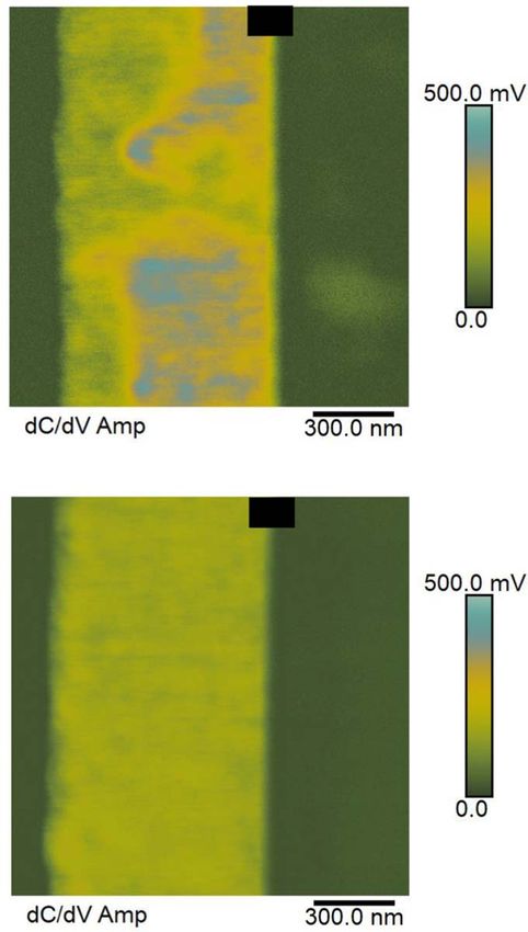
Nano Express 2 (2021) 010037                                                                                        R C Germanicus et al

   Figure 1. Scanning Electron Microscopy views of the used probes (a) Pt/Ir coated highly n-doped silicon probe SCM-PIC (b) highly
   conductive full diamond Adama tip (AD-40-AS) for SSRM measurements.

   Figure 2. Nano-MIS and nano-Schottky of the SCM and SSRM modes, respectively, with their respective equivalent circuits.

    Using SCM, the nano-contact between the conductive tip and the sample provides a nanometer-sized Metal-
Insulator-Semiconductor (MIS) capacitor structure [14–16] (figure 2). Here, the metallic electrode is the tip, the
semiconducting electrode is the sample, and the necessary insulator is a thin oxide layer being created on the
sample surface by a controlled thermal oxidation step. The capacitance of the nano-MIS is controlled by an
applied DC voltage bias (VDC) on the sample, while the tip is grounded. In addition, a low frequency (around
100 kHz) AC voltage (VAC) generates the capacitance variation of the free carriers of the sample under the local
contact. This local capacitance-voltage variation (¶C /¶V ) is recorded while the tip scans the surface of the

                                                       2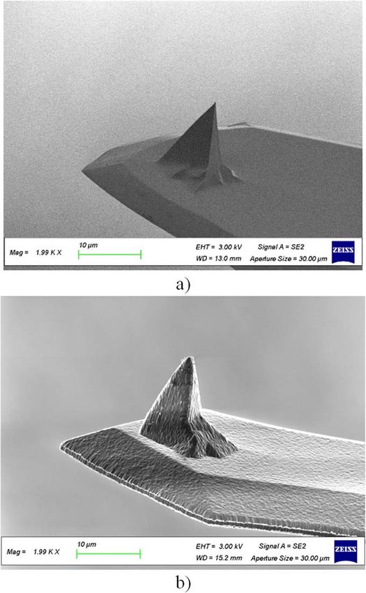
Nano Express 2 (2021) 010037                                                                        R C Germanicus et al

sample, under different VDC, allowing to identify the working regime (depletion, accumulation) of the nano-
MIS and therefore the locally present active dopant type and concentration. Thus SCM provides 2D maps of
local dopant activities.
     For SSRM measurements, the conductive AFM tip is in direct contact with the analyzed surface and forms a
nano-Schottky (Metal-Semiconductor) contact [9, 17, 18] (figure 2). Using a logarithmic amplifier with a
dynamic range of seven orders of magnitude, the current flowing from the tip through the sample to the back-
contact is recorded at each pixel, when a DC bias is applied between the tip and the sample back contact. For
silicon, during SSRM measurements, a highly stressed region just below the tip is necessary to create the
conductive β-tin silicon phase [19–21]. Therefore, SSRM measurements are carried out with a strong tip-sample
contact, applying the necessary mechanical pressure [19]. Using ultra-hard tips (doped diamond) allows to avoid
the deformation of the tip during the measurements and to guarantee the reliability of the generated data [22].
The equivalent model of this nanocontact is a sum of resistances in series: the tip resistance, the spreading
resistance of the nano-Schottky contact, the contact resistance between the probe and the sample, the bulk
resistance of the sample and the back-contact resistance [23, 24]. For a stable tip and a stable electrical contact of
the sample with the AFM chuck, the tip, bulk and back-contacts resistances can be represented by a unique
constant resistance; RConstant (figure 2). The local resistance of the sample is therefore the unique locally varying
magnitude, and its variation can be imaged locally by the SSRM measurements to record 2D-maps of the local
resistance. Three dimensional procedures have been also reported [17, 25–27].
     For both SCM and SSRM modes, the obtained 2D acquisition maps consist in an image of the tip-sample
system’s electrical response a fixed set of AFM operating conditions (effective tip-sample contact area, applied
force, DC bias, AC bias, frequency K). For crystalline doped layers, for dopant concentrations from 1015 to 1020
at cm−3, a good reproducibility with high spatial resolution have been demonstrated [28–31].
     Nowadays, highly integrated semiconductor technologies aim at co-integrate many different devices, both of
a two-dimensional (planar) and three-dimensional (vertical) type, simultaneously on or in the same substrate.
During the semiconductor processing, two main issues appear during the layer deposition steps: first, deposition
uniformity in the vertical structures (pores, columns, K) and second, the control of mechanical deformation of
the wafer (also called wafer warpage) due to the strain introduced by the deposited layers. Depending on their
size and density, the vertical structures may have an important effect on the mechanical stability of the wafer, so
that the deposition uniformity and the wafer warpage may differ both through the deposition furnace load and
along the position on a single wafer. Therefore, the homogeneity in terms of layer thickness and electrical
properties inside a given wafer (intra-wafer uniformity) but also along the different simultaneously processed
wafers (inter-wafer uniformity) must be controlled and optimized. Resulting non-uniformities can concern
either the layer thicknesses and the filling of the 3D structures. In addition, when the process includes several
deep three-dimensional patterns and therefore weakening of the mechanical robustness of the wafer, critical
wafer warpage can occur, leading to handling problems or wafer breakage and thus to significant line-yield falls.
In order to avoid such problems, polycrystalline materials were often selected for the device fabrication. Layers
exhibiting polycrystalline character represent the best trade-off between structure filling, wafer warpage,
thickness uniformity and uniform electrical properties. Moreover, since uniform conductivity performances are
required, an in situ doping technique is preferred over the classical implantation doping [32]. Fabricated as
multiple layers, global electronic and mechanical properties are strongly dependent on the microstructure and
internal phases of the used materials.
     In order to study the electrical activation of dopant atoms by SCM and SSRM, we investigated a well-known
in situ doped polycrystalline silicon (polysilicon) films. Electrical transport properties of polysilicon material
have been understood for decades [33–36] and has enabled numerous applications in high integrated circuit and
solar cells [37]. At the grain boundaries trapping centers of carriers and minority carriers’ potential barriers have
been researched to control the electrical efficiency of the deposited layer. The control of the microstructure
[38, 39], electrical [40, 41] and mechanical properties of the polysilicon layer are of great importance in
microelectronics because of their direct link with device performances and buckling failures at the wafer level. In
order to minimize the device contact resistances [42], and to enhance carrier mobility and device drive current,
semiconductor layers with high concentration (higher than 1020 cm3) are used. Deposited on an ultrathin SiOx
layer, a passivating contact is created, this structure is designed as a tunnel oxide passivating contact [43, 44].
     In this context, we show that SCM and SSRM modes are perfect tools to provide answers to scientific and
technological issues for semiconductor devices, especially for highly doped layers. In a previous study, we have
demonstrated that AFM electrical modes allow to map the as-deposited polysilicon layer (with a phosphorus
doping concentration of 1020 at cm−3) [45]. Here, we go further by studying the nano-contact between the AFM
tip and the sample to fully exploit the SCM and SSRM modes for both as deposited and annealed films. The goal
is to highlight the capability of electrical modes based on AFM to mapping the dopant activation. The silicon
layer is deposited with a polycrystalline in situ doped structure, with a high (>1020 at cm−3) phosphorus dopant
concentration. For this, the macroscopic properties of the layers such as the average wafer stress, layer resistivity

                                               3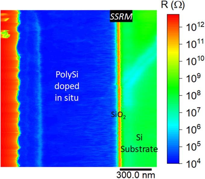
Nano Express 2 (2021) 010037 R C Germanicus et al
evolution and Hall conductivities are determined. We analyze in this work, the close link between the
microstructure and local electrical properties of a doped Low Pressure Chemical Vapor Deposition (LPCVD)
polysilicon. The evolution of the microstructure after the annealing step is investigated using x-Ray Diffraction
(XRD) combined analysis with MAUD software. This analysis allows to determine the anisotropic crystallite
shape, crystalline texture, unit cell parameters and thickness of the polycrystalline films. The local properties of
the layers are investigated by SCM and SSRM measurements, allowing for an insight on the nanoscale level, but
also a comparison with the chemical doping compositions of the layers obtained by Secondary Ions Mass
Spectroscopy (SIMS).
2. Experimental aspects
2.1. Materials
As substrate, (100) oriented, p-type (boron doped) single crystal silicon wafers were used. A silicon dioxide layer
of 100 nm was grown on these substrates by wet thermal oxidation. Then, the highly in situ phosphorous doped
polysilicon films were deposited by LPCVD with a total thickness around 750 nm. Note that, here we focus on
the local measurement of the dopant activity of the highly in situ doped polysilicon, the used SiO2 layer is
relatively thick. These depositions were carried out in a conventional horizontal furnace, a horizontal hot wall
reactor from THERMCO (5200 Series) with fused silica tube and liner, and silicon carbide wafer holder. For
these experiments, the dilution ratio of phosphine (PH3) in silane (SiH4) has been fixed at 5×10⁻³. A pressure
of 26.6 Pa is used, and deposition temperatures varied from 560 °C to 635 °C.
The annealing steps were performed in a conventional horizontal furnace. In order to preserve the electrical
properties of the as-deposited layers, a first annealing step is a low-temperature oxidation step under O2
followed by a high-temperature step (under N2). This way, a capping layer of polysilicon oxide is created at the
surface. Afterwards, the wafers were annealed at 1000 °C during 40 min to achieve a homogeneous dopant
redistribution and activation.
2.2. Characterization techniques
Polysilicon layer resistivities were determined from their resistance (measured by a four points probe
equipment, Prometrix Omnimap RS35C) and thickness (measured by optical reflectometer, Nanospec
AFT 4000).
A FSM8800 curvature measurement system based on laser beam deflection was used to investigate the
warpage. The average residual film stress in the polysilicon films is calculated, with the assumption of an
isotropic distribution and the biaxial rotationally symmetric stress case, by the Stoney’s equation [46]
Es ts2 ⎛ 1 1 ⎞
s= ⎜ - ⎟ (1)
6(1 - ns ) t ⎝ R a Rb ⎠
where Es is the Young’s modulus (1.3×10¹¹ Pa) and υs the Poisson’s ratio (0.28) of pure silicon, ts and t the
thickness of the silicon wafer and deposited film respectively, and Ra and Rb the measured radius of curvature
after and before deposition, respectively.
Hall measurements were carried out on square pieces of 0.25 cm2 obtained by cleavage. Four alumina
contacts were deposited in the corners of the sample by evaporation and the electrical contact was achieved using
wire bonding.
Quantitative analyses of the crystallographic textures and microstructures at the film scale was probed using
4-circles x-ray diffractometry with a setup equipped with monochromatized CuKα radiation and a Curved
Position Sensitive detector (CPS120 from ThermoFisher Scientific), described in details elsewhere [47]. The
typical analyzed surface is of several mm2, and the whole thickness of the layer is probed. We used the Combined
Analysis formalism based on Full-Powder-Pattern Rietveld refinement [48], as implemented in the MAUD
software [49], to determine simultaneously the textures and microstructures. Briefly, this methodology uses an
extended cyclic Rietveld refinement of a series of x-ray diagrams measured at different sample orientations. We
measured 936 diagrams every 5° in tilt an azimuth angles (χ and j respectively), varying in the 0–60° and 0–355°
ranges respectively, and for an incident angle of the x-ray beam on the sample of 20°. The instrument
contributions (χ and ω broadenings, peak shapes, zero-shifts) were calibrated using the 660 srmb LaB6 powder
standard from NIST. A counting time of ten seconds for each sample orientation was used, and our optical setup
provides with a 0.1° peak width in 2θ around 30°. Pole figures obtained are normalized into multiples of a
random distribution (m.r.d). In such m.r.d units, a sample without preferred orientation exhibits uniform pole
figures with 1 m.r.d levels, while a textured sample shows pole figures with maxima and minima of orientation
densities ranging from 0 m.r.d (absence of crystals oriented in this direction) to infinity (for a single crystal on
4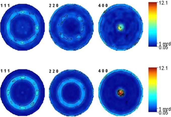
Nano Express 2 (2021) 010037 R C Germanicus et al
Figure 3. Impact of the deposition temperature of in situ doped LPCVD polysilicon layers (for 6 inch silicon wafers) before and after
annealing: (a) layer resistivity and (b) residual stresses.
few directions). The overall texture strength is evaluated through the texture index [49]. The normalized pole
figures are calculated from the orientation distribution (OD) of crystallites, refined using the E-WIMV
formalism after extraction of the peak intensities during the Rietveld cycles using the Le Bail approach. The OD
and profile refinement reliabilities are estimated using conventional reliability factors.
The doping profiles along the layer thickness were obtained from phosphorus SIMS depth profiles using Cs+
primary ions at 10 keV energy. Calibration of the SIMS apparatus was achieved with a phosphorus standard and
the analyzed area was about 150 μm2.
AFM measurements were performed using a Dimension AFM (Bruker) operated at room temperature. A
vibration-free table was used to eliminate any ground vibrations and/or acoustic noise. Tapping mode is used to
acquire the topography. For SCM measurements, a Pt/Ir coated highly n-doped silicon probe (SCM-PIC) was
employed. SSRM measurements were conducted with a highly conductive full diamond tip of Adama with an
apex of 10 nm (AD-40-AS). The stiffness of the cantilever was determined by the thermal tune method, the
spring constant of the cantilever of the used probe was 42 N/m. Force curves have been performed on a sapphire
in contact mode to measure the sensitivity of the cantilever. Forr all electrical measurements, the scan rate was
0.5 Hz. All maps are recorded with a resolution of 512×512 pixels. Before and after each study, the tip apex
integrity is checked either with SEM analysis (figure 1) or with a calibrating sample.
For the SCM and SSRM experiments, cross-sections of the samples were prepared. The sample was glued to a
sample holder on the film side for protection, and the cross-sectional surface was then mechanically polished as
to obtain a smooth surface. Successive polishing steps first with SiC paper with decreasing grain size down to
0.1 μm and then with colloidal solutions were done, until a mirror-like surface was obtained. For the SCM
measurements, the cross section was annealed to obtain a native oxide layer. This annealing step was carried out
at 270 °C during 30 min. The thickness of the obtained oxide layer is estimated to be around 3 nm.
5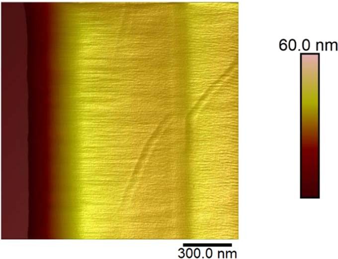
Nano Express 2 (2021) 010037                                                                                          R C Germanicus et al

   Figure 4. (a) Sum of the 936 diffraction diagrams of the sample and (b) 2D representation of all measured (bottom) and refined (top)
   diagrams showing the texture in the films (along the vertical axis are developed 936 experimental and 936 refined diagrams for as
   many (χ,j) orientations).

3. Macroscopic characterizations: resistivity and stress

As function of parameters deposition, electrical properties are important parameters to control. In a first part,
we compare the quantification of the properties (global resistivity, residual stress and microstructure) of the as-
deposited highly in situ doped polysilicon layer before and after the annealing step. The evolution of the
resistivity of the as-deposited layers as a function of the LPCVD deposition temperature is given in figure 3(a)).
The smooth evolution of the resistivity with the deposition temperature indicates the absence of any structural
transformation, but it seems also that the doping species incorporation (from an electrical point of view) within
the crystal lattice is better at low deposition temperatures, probably linked to the enhanced grain growth. In fact,
lower deposition temperatures favor the grain growth over nucleation, leading to larger grains. Therefore, it
decreases the grain boundary density, inducing less defects in the films. Finally, it enables larger doping
efficiencies and reduces charge carriers scattering, decreasing the film resistivity.
    To activate the dopant in the polysilicon layer, three wafer sets were annealed as described in the
experimental section. A resistivity in the order of 10–3 Ω.cm is achieved after annealing for all initial deposition
temperatures, showing that the annealing process is homogeneous for all the polycristaline films.

                                                        6
Nano Express 2 (2021) 010037                                                                                              R C Germanicus et al

   Figure 5. Normalized pole figures for the three main crystallite directions of polysilicon as deposited and after annealing.

    In addition, during the manufacturing process, the electrical properties are not the only parameter to be
taken into account to determine the optimized deposition parameters. In fact, for strongly thinned wafers or for
high densities of 3D structures, a wafer deformation may have a severe impact during the fabrication process.
The residual stress of the as-deposited films is represented in figure 3(b)). For all deposition temperatures, the
residual stress of the layer is compressive, with an only small variation.
    The high temperature annealing also significantly reduces the film stress to a moderate tensile stress of about
25 MPa. Therefore, the annealing process leads to the activation of the dopant in the polycrystalline film and an
important reduction of the residual strain independently on the initial deposition temperature.
    In the following, we will focus on the sudy of the LPCVD film deposited at 635 °C.

4. Microstructure characterization

X-Ray Diffraction (XRD) combined analysis were performed to reveal the texture and the structure of the
polysilicon layers [48, 50]. Mean crystallite anisotropic shape and sizes, cell parameter and quantitative
crystallographic textures are calculated from XRD measurements. Combined analysis Measurements and fits are
presented for the sum of all measured diagrams (figure 4(a)) and for all diagrams as a 2D plot (figure 6(b)).
Calculated and observed diagrams favorably compare, with relatively low reliability factors and GoF (Goodness-
of-Fit) values for the whole set of 936 diagrams (table 1). The film structure is consistent with a regular diamond
cubic structure of silicon with a cell parameter around 5.43 Å. When tilting the samples, significant peak shifts
could be observed, indicating stabilization of residual strains in the films. The cell parameter value given here
corresponds to the refined relaxed state, provided by the combined analysis approach. It is then the cell
parameter of the unstrained film which would have been prepared using exactly the same conditions. The
refined values are always larger than those for bulk silicon.
    The as-deposited sample exhibits small mean crystallite sizes (i.e. mean coherent size domains) of about
120 Å and quasi isotropic shapes (with an anisotropic shape factor Г very close to 1). The annealing induces a
strong grain growth and the development of an enhanced texture. According to our measurements, annealed
samples present [111]-elongated crystallites with a largest dimension reaching 6400 Å and a larger anisotropic
shape ratio. It results in ellipsoidal shaped crystallites whose largest length is along the [111] direction. Regarding
crystallographic texture (figure 5), the {400} pole figures exhibit a maximum distribution density value in their
center, corresponding to the normal Z to the film plane. Another large density value is observed on a ring along
the equator of these pole figures, showing then the existence of a ⟨100⟩-cyclic-fiber texture component, with the
⟨100⟩ fiber axis being aligned with Z. From the three recalculated and normalized pole figures this texture
component seems to be major, and an important amount of crystallites are then aligned with their ⟨100⟩
direction parallel to Z of the substrate. However, the ring observed on the equator of {400} is deviating slightly
from perfect homogeneity, along the X and Y directions of the sample corresponding to the main axes of the
substrate. It then exists also a minor orientation component corresponding to a kind of epitaxial relationship
with the substrate defined by ⟨100⟩-polysilicon//[100]-Si. These two components of orientation are observed as
well in as-deposited as in annealed samples. After annealing, the pole figure exhibits enhanced orientation
densities. It appears that the highest density is reached in the center of the {400} pole figure (12.1 m.r.d). From

                                                          7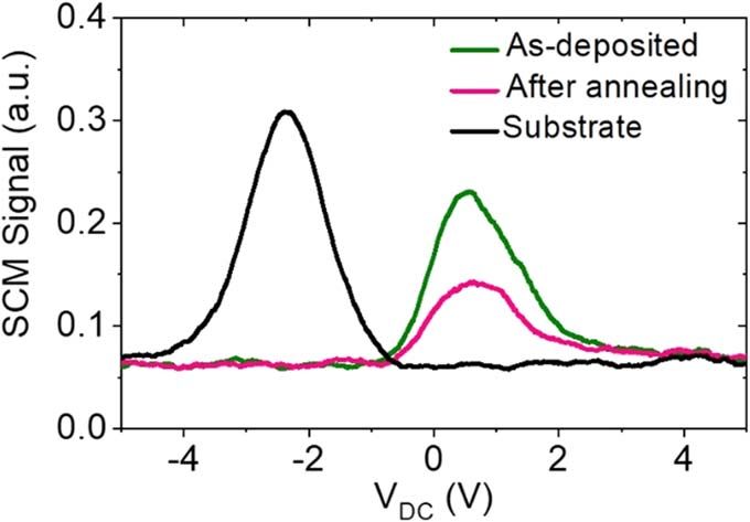
Nano Express 2 (2021) 010037 R C Germanicus et al
Figure 6. Surface topography (1.5 μm×1.5 μm) of the cross-sectional sample. The profile of the surface is added in black.
Figure 7. 2D Power spectral density (PSD) as a function of spatial frequency. for the AFM topography acquisitions (1.5 μm×1.5 μm)
of the as-deposited and annealed samples. The linear fitting (semi-logarithmic plot) is added in black.
Table 1. Structural and microstructural parameters of the films resulting from the Combined Analysis refinement. a: cell parameter. Δa and
Δa/a: absolute and relative difference in cell parameter from bulk silicon (5.43088 Å). thickness values from interferometry measurements.
Г: grain shape anisotropy factor. maximum and minimum orientation densities on the {100} pole figures. F2: texture index. Reliability
standard R-factors for the refinements: Rw : weighted. Rexp : experimental. GoF=(Rw/Rexp)2.
Sample As-deposited After annealing
Film thickness (nm) 759 761
Lattice parameter a (Å) 5.43109 (6) 5.43566 (2)
Δa (Å) −0.00021 −0.00478
Δa/a (%) −0.004 (6) −0.088 (2)
Anisotropic (i.e. cristallite) size [111] 122.9 (2) 6388 (77)
[220] 118.7 (2) 973 (35)
Γ=[111]/[220] 1.03 6.52
Texture parameters Max (m.r.d.) 7.5 12.1
Min (m.r.d.) 0.05 0.06
F2 (m.r.d.)2 20.42 20.38
Confience factors (%) Rw 22.3 23.5
Rexp 18.6 18.7
GoF (Rw/Rexp)2 1.44 1.58
8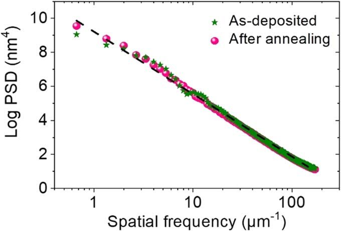
Nano Express 2 (2021) 010037 R C Germanicus et al
Figure 8. (a) C-V simulations of the nano-MIS contact for different doping levels. (b) dC/dV curves calculated from the simulations
with the same color-code for the doping levels as in (a). the inset shows the case of the highly doped silicon. 2D TCAD simulations for a
n-type layer with a charge concentration 2×1020 cm−3 for VDC=+ 0.5 V (c) and for VDC=− 0.5 V (d).
9Nano Express 2 (2021) 010037 R C Germanicus et al
Figure 9. ¶C/¶V versus VDC measured before and after annealing. the signal of the substrate is also added.
x-ray analysis, we demonstrate that the annealing process then favors the achievement of larger texture strengths
in the films.
The crystalline structure was studied using XRD measurements. and shows a polycrystalline character with a
main grain size about 123 Å in the [111] direction and 119 Å for the [220] direction before annealing. with a grain
shape anisotropy factor of about 1.03. After annealing. the combined analysis showed that the grain size of the
polysilicon increases by a factor of 52 in the [111] direction and of 8 for [220] direction. With XRD
investigations. the crystallization effect was investigated and we have proved that after annealing polysilicon
grains are significantly larger. This 3-D enlarge was also quantify. We assume that larger grains may explain the
differences in terms of electrical performances noticed by the layer resistivity. After annealing. doping atoms
may be more efficient and electrons may thus be more mobile. Then to study the local electrical properties.
electrical measurements on AFM were performed.
5. Local electrical characterization
The topography of the layer after annealing is represented in figure 6. Despite the presence of some stripes due to
the polishing process. we obtain a roughness in the polysilicon layer of Sq=1.8 nm and Sa=1.3 nm (statistical
parameters calculated with the standard ISO 25178 [51]). This high-quality surface is in perfect adequation with
nano-electrical modes in contact to ensure electrical stability [52]. Furthermore. the Power Spectral Density
(PSD) analysis have been performed for the surfaces of the cross-sections of the samples before and after
annealing [53, 54]. Figure 7 displays the 2D PSD curves obtained for the two samples. The two PSD curves show
the same evolution as the fonction of the spatial frequency. The linear fitting of the semi-logarithmic plot is
added. We can note a small difference at low frequencies (corresponding to large superficial features). probably
due to the topographical change at the layer surface of the cross-section. related to the prxence of the glue. On the
other hand. at high frequencies (above 10 μm−1) the curves are superimposed. the two samples present similar
roughness.
For this highly doped layer. we have simulated the nano-electrical MIS contact with TCAD tools in order
identify the extention of the measured properties with high precision. The conductive AFM tip in contact with
the doped silicon layer was modelled as a nano-MOS structure. A planar contact with symmetry around the tip
axis is simulated. the tip radius is 20 nm.
The thickness of the oxide layer on top of the cross-sectional sample was fixed to 3 nm. corresponding to the
thickness estimation based on the preparation method of the cross-section. The simulations were carried out for
silicon (n- and p-type) and a metal contact at the bottom was added to simulate the contact with the chuck.
Thereby. the C-V curves are generated for different doping concentrations (figure 8(a)). The simulations have
been done with a voltage sweep starting from negative biases (−5V) towards positive biases (+5V). The bias
simulated here (VMOS) is the inverse of the bias VDC applied to the AFM chuck during measurements. As
expected. the shape of the C-V curves depends on the doping concentration and the type of the silicon substrate.
These simulated curves are in accordance with previous works [16, 55, 56]. Based on the SCM methodology. the
doping concentration increase induces a decrease of the slope of the C-V curves and a shift of the position of the
inflexion point of the curve. In order to highlight the strong impact of the VDC voltage during the measurement
of the highly doped polysilicon layer. the simulated dC/dV curves are displayed in figures 8(b) for different
10Nano Express 2 (2021) 010037 R C Germanicus et al Figure 10. SCM maps (1.5 μm×1.5 μm) on the cross sectionnal sample (a) for the as-deposited n++ polysilicon layer and (b) after annealing. doping levels (the high doping levels are shown in the inset). As we can see. when the doping level increases. the the derivative capacitance drops drastically. Therefore. in the present work. since the material is highly doped (
Nano Express 2 (2021) 010037 R C Germanicus et al
Figure 11. Force-curve and SSRM signal as a function of the force applied to the cantilever.
of the SCM signal decreases. Since ∂C/∂V is inversely proportional to the active doping level of the
semiconductor. this behavior indicates clearly a increase of the active dopant concentrations in the polysilicon
layer after the annealing step in perfect agreement with the simulations. For a positioning of the tip on the p-type
substrate. the SCM signal shows a maximum at negative DC sample bias. according to the C-V change simulated
by TCAD (figure 8(a)). Thus the control of the applied VDC during SCM experiments plays a crucial role in the
interpretating measured signal. This point is very important and even more for highly doping layer since the flat
band voltage is shifted from 0 V.
Based on these results. an applied VDC bias of 0 .5 V and VAC=1 V is chosen for the comparison of the
polysilicon 2D SCM mappings. The obtained SCM maps of the in situ doped polysilicon layer before and after
annealing are shown in figure 10. In both acquisitions. the polysilicon layer can be clearly distinguished from the
p-type substrate. due to the strong ∂C/∂V contrast at the chosen VDC bias. The corrugated surfaces of the
polysilicon materials at the interfaces with the glue (used to fabricate the cross-sectional samples) are related to
the crystalline nature of polysilicon grains determined by XRD investigations. By comparing the two maps. the
modification of the carrier distribution and activation during the annealing can be clearly observed. In fact.
before annealing. the polysilicon layer presents a non-homogeneous doping carrier concentration of the active
dopants concentration along the layer. After annealing. the polysilicon layer shows a uniform active dopant
distribution in the bulk of the layer. and a smooth interface with the substrate. The oxide layer at the interface
with the wafer seems to be slightly better defined. translating an electrical activation of the dopants reaching the
polysilicon/oxide layer without any charge-depleted zone in the polysilicon layer. Also. at the surface of the
polysilicon layer after annealing. a well-defined charge depleted region can be observed. corresponding to the
oxide layer created before the principal annealing step in order to avoid the out-diffusion of the dopants.
SSRM is also deployed to analyse the activation of the dopant in the semiconductor layer. To carry out SSRM
measurements with a high control. it is very important to control the tip-semiconductor contact [17, 24]. To
quantify the force to be applied to the cantilever in order to create the β-tin pocket under the tip. a force curve
was recorded on the polysilicon layer. with the corresponding measured resistance. In figure 11. we have
represented both the force curve and the SSRM signal as a function of the Z position of the AFM piezoelectric
displacement. Far from the sample. the SSRM resistance is larger than 1015 Ω because of the absence of contact.
Afterward. the cantilever is pulled down towards to contact the silicon surface (at the point B). At this
displacement of 350 nm. the tip-sample contact is established. indicated by a change of slope in the force curve.
With a further increase of the displacement. the diamond tip starts to penetrate the sample. Interestingly. a
further displacement of 37 nm is neccesary before the electrical resistance (SSRM signal) drops. This behaviour is
the signature of the creation of the highly stressed β-tin region just below the tip contact. It is important to note
that this distance corresponds to the displacement of the Z-piezo and represents the cantilever deflection and the
effective penetration of the SSRM tip in the surface. The reaction of the cantilever has to be taken into account. so
that the real penetration of the tip in the sample is smaller. When the force increases further. the resistance drops
until reaching a plateau (D). The tip resistance contibution was measured in a conductive material (aluminium
layer on another sample). the value is lower than 104 Ω.
With this calibration step. the scanned parameters for SSRM were fixed at 2.5 μN applied to the cantilever
and a VDC of 600 mV. During measurement. we verified the stability of the signal with the applied VDC.
12Nano Express 2 (2021) 010037 R C Germanicus et al
Figure 12. SSRM map of the cross sectional sample. scan size : 1.5 μm×1.5 μm.
Table 2. Mean values for Phosphorus concentration from Hall Effect measurements.
Phosphorus atoms concentration from Hall Phosphorus atoms concentration from Doping Efficiency (%)
effect measurements (cm−3) Electrically SIMS measurements (cm−3) Total amount Active carriers/Total
Sample active charge carriers of doping species carriers
As-deposited 8.1×10¹⁹ 2.5×10²⁰ 32
After annealing 2.4×10²⁰ 2.7×10²⁰ 89
according the procedure presented in [17]. The SSRM map for the sample after annealing is represented in
figure 12. in a 2D top view.
Again. the SSRM maps show a strong contrast between the substrate and the polysilicon layer. related to the
change in dopant concentration. The polysilicon layer itself shows a homogeneous resistance through the bulk
of the film. although some contrast is visible in the top part of the layer. At the interface with the glue. the SSRM
contrast is correlated with the topography of the cross-sectional sample (figure 6): the curvature at the top of the
layer (due to the polishing step) induces a change in the tip contact area and the exerted force. leading to this
contrast. Also. at the surface of the polysilicon layer. the insulating region can be identified (light blue region at
the top). This insulating region is related to the oxidation step in the annealing procedure. creating an oxide layer
in order to trap the dopants. The SSRM mapping allows therefore to estimate the thickness of this layer to be
around 45 nm. Furthermore. the oxide layer at the polysilicon/wafer interface can be distinguished clearly due
to its insulating character. a high resistance is measured.
To complete the electrical investigations. the total phosphorus doping concentration for as-deposited and
annealed samples was determined by SIMS (chemical analysis) on cross-sectional samples. The mean value of
phosphorus concentration measured inside the layers before and after annealing are compared with Hall effect
measurements in table 2. The dopant efficiency for the in situ doped layer is determined. showing that while only
32% of the dopants are active in the as-deposited state. close to 90% participate in electrical transport after the
annealing step.
To highlight the complementarity of the SCM and SSRM modes. the profiles of SIMS. AFM electrical modes
are compared in figure 13. Based on the detection of phosphorus atoms. the SIMS measurement allows for a 1D
depth analysis. Despite its excellent accuracy. SIMS is limited to the chemical information of the material. In the
case of activated dopants as in polysilicon material. the chemical information (presence of the chemical species)
is different from the active carrier concentrations in the layer. In fact. the change observed in the Hall effect
carrier concentration underlines the electrical activation of the P dopants during the annealing steps. As can be
observed in figure 13. the SCM profiles show clearly the change in active doping concentrations before and after
the annealing.
13Nano Express 2 (2021) 010037 R C Germanicus et al
Figure 13. SIMS. SCM (phase and amplitude) and SSRM profiles before and after annealing.
But even more. the chemical signature (SIMS profiles) of the phosphorus concentration remains unchanged
after activation of the dopants. i.e. annealing. Thus. the annealing does not have an effect on the distribution of
the dopants. only on activation of their charges. The electrical characteristics related to the transport properties
of the polysilicon layer deposited on the oxide layer and the p-type substrate are clearly determined by SCM and
SSRM. The results of the two modes. when executed carefully. can be compared directly. The SCM and the
SSRM profiles allow therefore to estimate the electrical thickness of the polysilicon layer to be around 765 nm.
Therefore. based on a nano-MIS and a nano-Schottky properties. we demonstrated the complementary of the
SCM and SSRM. respectively. to analyze highly doped and nano-structured films. As the conductive tip in
contact with the analyzed surface represents a singular nano-object. our results show clearly that the control of
the AFM parameters: tip properties. applied force. applied VDC voltages during SCM and SSRM measurements
allows to determine the dopant activity of the passivating contact. Furthermore. to finely control transport
properties of materials. SCM and SSRM are complementary to the chemical compositions analysis obtained by
SIMS. TOF-SIMS or Atom Probe Tomography (ATP).
14Nano Express 2 (2021) 010037 R C Germanicus et al
6. Conclusion
The macroscopic and local structural and electric properties of a highly n-doped polysilicon LPCVD layer were
investigated before and after the annealing step regarding the distribution and the activation of the dopants. The
annealed layers show optimized properties for co-integrated device technologies and also for the filling of high
aspect ratio 3D structures. as well as to achieve low resistance contacts and low passivating contacts. With a stress
level of − 25 MPa of the annealed film. wafer warpage can be minimized. In addition. the mean macroscopic
resistivity decreases by the annealing. from 8×10⁻³ Ω·cm to 7.3×10⁻⁴ Ω·cm. while the Hall mobility
increased from 9.2 to 35.4 cm2/V·s. Combined XRD measurements revealed that grain growing occurs
preferentially along [111] axis whose highest dimension of elongated crystallites reach 6400 Å.
The analysis of the local properties. by SCM and SSRM. reveals a homogeneous active dopant distribution
throughout the layer after annealing. These insights cannot be obtained by the combination of macroscopic
characterization techniques or chemical analysis. underlining the interest of local electrical modes based on
AFM. But even more. the two applied electrical modes. SCM and SSRM. are clearly complementary due to the
contact formed between the tip and the sample. With the MIS-contact in the SCM mode. the SCM signal is
sensitive to the active dopant distribution. through the modulation of the bias voltage. On the other hand.
although employed at its detection limit due to the strong doping of the polysilicon layer. the SSRM signal using
a tip-sample contact of the Schottky type. allows to extract the local resistivity and detect local resistivity
variations. Here. insulating parts of the sample. as the oxide interface layer. can be localized. By compiling all
results. we concluded that electrical transport investigations based on AFM are key parameters to reveal dopant
activation in nano-structured films. even very heavily doped.
Acknowledgments
The authors would like to thank INSA Toulouse for SIMS measurements. as well as S. Froissart and X. Larose for
the SEM views of the tips. The authors also thank the Région de Normandie and European Regional
Development Fund for financial support in the framework of the RIN project PlaceNano No. 18E01664/
18P02478.
Data availability statement
No new data were created or analysed in this study.
ORCID iDs
Rosine Coq Germanicus https://orcid.org/0000-0002-6698-4853
Daniel Chateigner https://orcid.org/0000-0001-7792-8702
Wadia Jouha https://orcid.org/0000-0003-0067-9407
Olivier Latry https://orcid.org/0000-0002-2121-8864
Ulrike Lüders https://orcid.org/0000-0002-5766-8031
References
[1] Vandervorst W, Fleischmann C, Bogdanowicz J, Franquet A, Celano U, Paredis K and Budrevich A 2017 Dopant. composition and
carrier profiling for 3D structures Mater. Sci. Semicond. Process. 62 31–48
[2] Oliver R A 2008 Advances in AFM for the electrical characterization of semiconductors Rep. Prog. Phys. 71 076501
[3] Hussain S, Xu K, Ye S, Lei L, Liu X, Xu R, Xie L and Cheng Z 2019 Local electrical characterization of two-dimensional materials with
functional atomic force microscopy Front. Phys. 14 33401
[4] Zhong J and Yan J 2016 Seeing is believing: atomic force microscopy imaging for nanomaterial research RSC Adv. 6 1103–21
[5] De Wolf P, Brazel E and Erickson A 2001 Electrical characterization of semiconductor materials and devices using scanning probe
microscopy Mater. Sci. Semicond. Process. 4 71–6
[6] Kopanski J J 2007 Scanning capacitance microscopy for electrical characterization of semiconductors and dielectrics Scanning Probe
Microscopy: Electrical and Electromechanical Phenomena at the Nanoscale ed S Kalinin and A Gruverman (New York. NY: Springer)
p 88–112
[7] Yamamoto T, Suzuki Y, Miyashita M, Sugimura H S H and Nakagiri N N N 1997 Scanning capacitance microscopy as a
characterization tool for semiconductor devices Jpn J. Appl. Phys. 36 1922
[8] Giannazzo F, Raineri V and Priolo F 2002 Two dimensional boron diffusion determination by scanning capacitance microscopy Mater.
Sci. Eng. B 91–92 220–3
[9] Eyben P, Vandervorst W, Alvarez D, Xu M and Fouchier M 2007 Probing semiconductor technology and devices with scanning
spreading resistance microscopy Scanning Probe Microscopy (New York. NY: Springer) pp 31–87
15Nano Express 2 (2021) 010037 R C Germanicus et al
[10] De Wolf P, Snauwaert J, Clarysse T, Vandervorst W and Hellemans L 1995 Characterization of a point‐contact on silicon using force
microscopy‐supported resistance measurements Appl. Phys. Lett. 66 1530–2
[11] Vandervorst W 2007 USJ metrology : from 0D to 3D analysis AIP Conf. Proc. 931 233–45
[12] Trenkler T et al 2000 Evaluating probes for ‘electrical’ atomic force microscopy J. Vac. Sci. Technol. B Microelectron. Nanometer Struct.
Process. Meas. Phenom. 18 418–27
[13] Álvarez D, Hartwich J, Fouchier M, Eyben P and Vandervorst W 2003 Sub-5-nm-spatial resolution in scanning spreading resistance
microscopy using full-diamond tips Appl. Phys. Lett. 82 1724–6
[14] Buh G H, Chung H J, Kim C K, Yi J H, Yoon I T and Kuk Y 2000 Imaging of a silicon pn junction under applied bias with scanning
capacitance microscopy and Kelvin probe force microscopy Appl. Phys. Lett. 77 106–8
[15] Edwards H, McGlothlin R, San Martin R U E, Gribelyuk M, Mahaffy R, Ken Shih C, List R S and Ukraintsev V A 1998 Scanning
capacitance spectroscopy: an analytical technique for pn-junction delineation in Si devices Appl. Phys. Lett. 72 698–700
[16] Murray H, Germanicus R, Doukkali A, Martin P, Domenges B and Descamps P 2007 Analytic description of scanning capacitance
microscopy J. Vac. Sci. Technol. B Microelectron. Nanometer Struct. Process. Meas. Phenom. 25 1340–52
[17] Coq Germanicus R, Leclère P, Guhel Y, Boudart B, Touboul A D, Descamps P, Hug E and Eyben P 2015 On the effects of a pressure
induced amorphous silicon layer on consecutive spreading resistance microscopy scans of doped silicon J. Appl. Phys. 117 244306
[18] Schulze A, Hantschel T, Dathe A, Eyben P, Ke X and Vandervorst W 2012 Electrical tomography using atomic force microscopy and its
application towards carbon nanotube-based interconnects Nanotechnology 23 305707
[19] Mylvaganam K, Zhang L C, Eyben P, Mody J and Vandervorst W 2009 Evolution of metastable phases in silicon during
nanoindentation: mechanism analysis and experimental verification Nanotechnology 20 305705
[20] Eyben P, Mody J, Vemula S C and Vandervorst W 2008 Impact of the environmental conditions on the electrical characteristics of
scanning spreading resistance microscopy J. Vac. Sci. Technol. B Microelectron. Nanometer Struct. Process. Meas. Phenom. 26 338–41
[21] Fouchier M, Eyben P, Alvarez D, Duhayon N, Xu M, Brongersma S, Lisoni J and Vandervorst W 2003 Fabrication of conductive atomic
force microscope probes and their evaluation for carrier mapping Smart Sensors. Actuators. and MEMS Smart Sensors. Actuators. and
MEMS 5116 (International Society for Optics and Photonics) 607–16
[22] Hantschel T, Demeulemeester C, Eyben P, Schulz V, Richard O, Bender H and Vandervorst W 2009 Conductive diamond tips with
sub-nanometer electrical resolution for characterization of nanoelectronics device structures Phys. Status Solidi a 206 2077–81
[23] Eyben P, Alvarez D, Clarysse T, Denis S and Vandervorst W 2003 Recent progress and insights in two‐dimensional carrier profiling
using scanning spreading resistance microscopy AIP Conf. Proc. 683 685–92
[24] Pandey K, Paredis K, Robson A J and Vandervorst W 2020 Understanding the effect of confinement in scanning spreading resistance
microscopy measurements J. Appl. Phys. 128 034303
[25] Prüßing J K, Böckendorf T, Hamdana G, Peiner E and Bracht H 2020 Defect distribution in boron doped silicon nanostructures
characterized by means of scanning spreading resistance microscopy J. Appl. Phys. 127 055703
[26] Eyben P et al 2019 3D-carrier profiling and parasitic resistance analysis in vertically stacked gate-all-around si nanowire CMOS
transistors 2019 IEEE Int. Electron Devices Meeting (IEDM) 2019 IEEE Int. Electron Devices Meeting (IEDM pp 3.1–3.4
[27] Mody J, Zschatzsch G, Kolling S, De Keersgieter A, Eneman G, Kambham A, Drijbooms C, Schulze A, Chiarella T and Horiguchi N
2011 3D-carrier profiling in FinFETs using scanning spreading resistance microscopy IEEE International Electron Devices Meeting,
Washington 6.1.1–6.1.4
[28] Fujita T, Matsumura K, Itoh H and Fujita D 2014 Analytical procedure for experimental quantification of carrier concentration in
semiconductor devices by using electric scanning probe microscopy Meas. Sci. Technol. 25 044021
[29] Ban D, Sargent E H, Dixon-Warren J St, Calder I, Grevatt T, Knight G and White J K 2002 Two-dimensional transverse cross-section
nanopotentiometry of actively driven buried-heterostructure multiple-quantum-well lasers J. Vac. Sci. Technol. B Microelectron.
Nanometer Struct. Process. Meas. Phenom. 20 2401–7
[30] Eyben P, Janssens T and Vandervorst W 2005 Scanning spreading resistance microscopy (SSRM) 2d carrier profiling for ultra-shallow
junction characterization in deep-submicron technologies Mater. Sci. Eng. B 124 45–53
[31] Eyben P, Vanhaeren D, Janssens T, Hantschel T, Vandervorst W, Adachi K and Ishimaru K 2007 Evaluation of the junction delineation
accuracy and reproducibility with the SSRM technique Microelectron. Eng. 84 437–40
[32] Calvo J, Drescher M, Kühnel K, Sauer B, Müller M, Schmidt C, Boui F, Völklein F and Wagner-Reetz M 2018 LPCVD in situ doped
silicon for thermoelectric applications Mater. Today Proc. 5 10249–56
[33] Seto J Y W 1975 The electrical properties of polycrystalline silicon films J. Appl. Phys. 46 5247–54
[34] Zaidi B, Hadjoudja B, Shekhar C, Chouial B, Li R, Madhava Rao M V, Gagui S and Chibani A 2016 Dopant segregation and heat
treatment effects on the electrical properties of polycrystalline Silicon thin Films Silicon 8 513–6
[35] Haddad Adel A, Inokuma T, Kurata Y and Hasegawa S 2005 Characterization of structure and role of different textures in
polycrystalline Si films J. Non-Cryst. Solids 351 2107–14
[36] Borisenko V E and Hesketh P J 1997 Crystallization. Impurity diffusion. and segregation in polycrystalline silicon Rapid Thermal
Processing of Semiconductors Microdevices ed V E Borisenko and P J Hesketh (Boston. MA: Springer) pp 93–111
[37] Park H et al 2019 Role of polysilicon in poly-Si/SiOx passivating contacts for high-efficiency silicon solar cells RSC Adv. 9 23261–6
[38] Temple-Boyer P, Rousset B and Scheid E 2010 Influences of deposition and crystallization kinetics on the properties of silicon films
deposited by low-pressure chemical vapour deposition from silane and disilane Thin Solid Films 518 6897–903
[39] Birkholz M, Selle B, Fuhs W, Christiansen S, Strunk H P and Reich R 2001 Amorphous-crystalline phase transition during the growth
of thin films: the case of microcrystalline silicon Phys. Rev. B 64 085402
[40] Dimitriadis C A, Stoemenos J, Coxon P A, Friligkos S, Antonopoulos J and Economou N A 1993 Effect of pressure on the growth of
crystallites of low‐pressure chemical‐vapor‐deposited polycrystalline silicon films and the effective electron mobility under high
normal field in thin‐film transistors J. Appl. Phys. 73 8402–11
[41] Mulder J G M, Eppenga P, Hendriks M and Tong J E 1990 An Industrial LPCVD process for In Situ phosphorus‐doped polysilicon
J. Electrochem. Soc. 137 273
[42] Mathad G S, Rathore H S and Arita Y 2000 Interconnect and Contact Metallization for ULSI: Proc. of the Int. Symp. (The Electrochemical
Society)
[43] Fong K C, Kho T C, Liang W, Chong T K, Ernst M, Walter D, Stocks M, Franklin E, McIntosh K and Blakers A 2018 Phosphorus
diffused LPCVD polysilicon passivated contacts with in situ low pressure oxidation Sol. Energy Mater. Sol. Cells 186 236–42
[44] Yang Q et al 2020 In-situ phosphorus-doped polysilicon prepared using rapid-thermal anneal (RTA) and its application for polysilicon
passivated-contact solar cells Sol. Energy Mater. Sol. Cells 210 110518
[45] Coq Germanicus R, Picard E, Domenges B, Danilo K and Rogel R 2007 Microstructure and electrical characterization based on AFM of
very high-doped polysilicon grains Appl. Surf. Sci. 253 6006–12
16Nano Express 2 (2021) 010037 R C Germanicus et al
[46] Freund L B and Suresh S 2004 Thin Film Materials: Stress. Defect Formation and Surface Evolution (Cambridge: Cambridge University
Press)
[47] Ricote J and Chateigner D 2004 Quantitative microstructural and texture characterization by x-ray diffraction of polycrystalline
ferroelectric thin films J. Appl. Crystallogr. 37 91–5
[48] Chateigner Daniel 2010 Combined Analysis (London: Wiley ) 978-1-84821-198-8 (https://doi.org/10.1002/9781118622506)
[49] Lutterotti L, Chateigner D, Ferrari S and Ricote J 2004 Texture. residual stress and structural analysis of thin films using a combined
x-ray analysis Thin Solid Films 450 34–41
[50] Morales M, Chateigner D and Lutterotti L 2009 X-ray textural and microstructural characterisations by using the combined analysis
approach for the optical optimisation of micro- and nano-structured thin films Thin Solid Films 517 6264–70
[51] Bonyár A 2016 AFM characterization of the shape of surface structures with localization factor Micron 87 1–9
[52] Goghero D, Raineri V and Giannazzo F 2002 Study of interface states and oxide quality to avoid contrast reversal in scanning
capacitance microscopy Appl. Phys. Lett. 81 1824–6
[53] Fiorenza P, Raineri V C, Ferrarelli M C, Sinclair D and Nigro R L 2011 Nanoscale electrical probing of heterogeneous ceramics: the case
of giant permittivity calcium copper titanate (CaCu 3 Ti 4 O 12 ) Nanoscale 3 1171–5
[54] Germanicus R C, Leclère P, Hug E, Lallemand F and Descamps P 2016 Statistical investigations of an ENIG nickel film morphology by
atomic force microscopy E3S Web Conf. 12 04003
[55] Giannazzo F, Goghero D and Raineri V 2004 Experimental aspects and modeling for quantitative measurements in scanning
capacitance microscopy J. Vac. Sci. Technol. B Microelectron. Nanometer Struct. Process. Meas. Phenom. 22 2391–7
[56] Stangoni M, Ciappa M and Fichtner W 2005 Assessment of the analytical capabilities of scanning capacitance and scanning spreading
resistance microscopy applied to semiconductor devices Microelectron. Reliab. 45 1532–7
17You can also read