Digital Twin for Secure Semiconductor Lifecycle Management: Prospects and Applications
←
→
Page content transcription
If your browser does not render page correctly, please read the page content below
FUTURE HARDWARE SECURITY RESEARCH SERIES

    Digital Twin for Secure Semiconductor Lifecycle
        Management: Prospects and Applications
        Hasan Al Shaikh, Mohammad Bin Monjil, Shigang Chen, Farimah Farahmandi, Navid Asadizanjani,
                                  Mark Tehranipoor, and Fahim Rahman
                    Email: {hasanalshaikh, monjil.m}@ufl.edu, Department of ECE, University of Florida
                           Email: sgchen@cise.ufl.edu, Department of CISE, University of Florida
         Email: {farimah, nasadi, tehranipoor, fahimrahman}@ece.ufl.edu, Department of ECE, University of Florida

    Abstract—The expansive globalization of the semiconductor                                    I. I NTRODUCTION
supply chain has introduced numerous untrusted entities into dif-
ferent stages of a device’s lifecycle, enabling them to compromise            Amidst rising threats in the supply chain and the ever ex-
its security. To make matters worse, the increasing complexity             panding attack surface, ensuring the security of semiconductor
in the design as well as aggressive time-to-market requirements
of the newer generation of integrated circuits can lead either             devices across their entire lifecycle has become a challenging
designers to unintentionally introduce security vulnerabilities or         and complex endeavor. Although established practice puts
verification engineers to fail in detecting them earlier in design         security at the forefront of each stage of the software develop-
lifecycle, often due to the limitation of traditional verification         ment lifecycle [1], such efforts to secure the hardware lifecycle
and testing methodologies. These overlooked or undetected vul-             is in its infancy due to the unique challenges associated with
nerabilities can be exploited by malicious entities in subsequent
stages of the lifecycle through an ever-widening variety of                it [2], [3]. The traditional hardware verification and testing
hardware attacks. The ability to ascertain the provenance of these         methodologies, that focus on functional verification as their
vulnerabilities, after they have been unearthed at a later stage,          primary objective, are often ineffective in detecting security
becomes a pressing issue when the security assurance across                vulnerabilities, which may be introduced through malicious
the whole lifecycle is required to be ensured and generationally           3PIPs, or security unaware design practices [4]. If security
improved to thwart emerging attacks.
    We posit that if there is a malicious or unintentional breach
                                                                           vulnerabilities evade detection and verification efforts, they
of security policies of a device, it will be reflected in the form         can later be exploited by malicious entities in the supply
of anomalies in the data collected through traditional design,             chain [5], [6]. Unlike software, however, hardware cannot be
verification, validation, and testing activities throughout the            easily patched, which makes identifying the root origin of
lifecycle. With that, a digital simulacrum of a device’s lifecycle,        the vulnerability in the silicon lifecycle paramount to ensure
called a digital twin (DT), can be formed by the data gathered
from different stages to secure the lifecycle of the device. The DT
                                                                           generational improvement in security assurance.
can analyze the collected data through its constituent AI and data            Digital twins (DT) have experienced exponential growth
analytics algorithms to trace the origin of a detected hardware            in academia as frameworks to monitor, maintain, and control
attack or vulnerability to the associated stage of the lifecycle. We       quality and reliability of different products across their differ-
refer to this functionality of the DT as Backward Trust Analysis.          ent stages of the lifecycle [7]. Although originally conceived
We also introduce the notion of Forward Trust Analysis which
refers to the scalability and adaptability of the DT to unforeseen         in [8] as a high fidelity digital representation of aerospace
threats as they emerge.                                                    vehicles, the concept and definition of the digital twin has
    In this paper, we put forward a realization of intertwined             evolved to encompass any virtual representation of a physical
relationships of security vulnerabilities with data available from         object, process, or operation which is continually updated
the silicon lifecycle and formulate different components of an AI          by data that is collected across the lifecycle using which
driven DT framework. The proposed DT framework leverages
these relationships to achieve aforementioned security objectives          it provides optimization feedback on the functionality and
through causality analysis, and thus accomplish end-to-end                 control of the physical counterpart (as shown in Figure 1
security-aware management of the entire semiconductor lifecycle.           [9]–[11]. Although DTs have received much recognition as
We put a perspective on how the limitations of existing ad-hoc-            tools of managing product maintenance, fault diagnosis, and
style security solutions can be overcome by the data oriented anal-        monitoring in the aerospace and manufacturing industry [12]–
ysis that underpins our approach. With several threat and attack
scenarios, we demonstrate how advanced modeling techniques                 [15], DTs that consider the full lifecycle are very rare. In fact,
can perform relational learning to identify such attacks. Finally,         Liu et al. report that only 5% of their reviewed papers on DTs
we provide potential future research avenues and challenges                considered the whole lifecycle [16]. Furthermore, addressing
for realization of the digital twin framework to enable secure             cyber and hardware security issues that are intertwined with
semiconductor lifecycle management.                                        cyber-physical systems utilizing DTs have also been rarely
    Index Terms—Digital twin, Hardware security & trust, Semi-
                                                                           considered [17].
conductor lifecycle management, Artificial intelligence, Root
cause analysis, Statistical relational learning, Electronic supply            Existing solutions proposed in academia and industry to
chain security, Backward & forward trust                                   address hardware security concerns also suffer from major

                                                                       1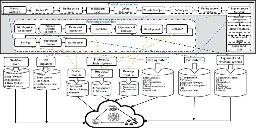
FUTURE HARDWARE SECURITY RESEARCH SERIES

Fig. 1. Digital twin components, functionalities, and bidirectional transactions for secure semiconductor lifecycle management. Blue colored boxes and circles
indicate components, controls, and transactions of a traditional DT framework focusing product monitoring and process optimization. The green colored boxes
and circles indicate those that required to be additionally incorporated into the framework for ensuring end-to-end security and assurance in semiconductor
lifecycle.

limitations when applied in the context of end-to-end secure                      solutions have the capability to trace the lifecycle stage where
lifecycle management. Firstly, almost all proposed detection                      it originated from. For example, if an information leakage is
and prevention mechanisms are concentrated on very specific                       detected through formal verification, existing methods cannot
threats at specific parts of the lifecycle [18], [19] with little                 infer whether the problem was introduced during high level
to no scalability when considering the entire lifecycle and                       architecture specification (also known as electronic system
other threat models. Secondly, although there are multiple                        level specification) or during the formulation of the logic
detection and prevention methods against hardware attacks                         design (through hardware description languages) of the circuit.
including hardware trojans [20]–[23], counterfeits [24]–[29],                     The ability to track down the origin is absolutely vital if
information leakage [30], [31], fault injection [32]–[34], and                    we want to facilitate generational improvement in security
side channel attacks [35]–[37], the analysis of these methods                     assurance of the design.
start with the a priori assumption that the defender knows                           Lastly, there have been suggestions in literature and the
what attack vector is principally responsible for an anomalous                    semiconductor industry to embed different types of sensors on
behavior. It is far more likely that the designer or defender                     the chip so that it has a defense against certain attack vectors
would only get to observe the anomalous behavior, rather                          [40], [41]. In addition to more area, power, and performance
than knowing what precise attack vector is causing said                           overhead, these approaches are not scalable in the context of
behavior. For example, from a hardware security perspective,                      emerging future threats. New threats and attack vectors are
a chip in a system may experience accelerated aging due to                        always being developed by researchers and malicious actors.
many possible reasons. It can fail before its intended lifespan                   As an example, in the initial years of hardware trojan research,
because i) it is a recycled chip that was unknowingly used                        it was frequently assumed that hardware trojans need to be
by the system designer, ii) it is a defective chip that was                       activated by rare signals and node to avoid detection. However,
shipped without authorization by an untrusted foundry or a                        researchers have since demonstrated that it is possible to
rogue employee working in a trusted foundry [38], or iii) it                      design hardware trojans that do not need be triggered by rare
experienced accelerated aging due to being taken over by a                        events yet easily escape traditional testing and verification
parametric hardware trojan [39]. Thirdly, once an attack or                       efforts [42]. It is not feasible to keep continually adding new
vulnerability has been detected, thus far none of the proposed                    sensors to a design to tackle new threats as they emerge.
                                                                                     Therefore, we argue that without a comprehensive frame-

                                                                              2
FUTURE HARDWARE SECURITY RESEARCH SERIES

work, such as the one we are proposing in this paper, security            lifecycle management and various DT applications proposed in
assurance in the semiconductor lifecycle would only be limited            cybersecurity and lifecycle management. Section III provides
to partial effectiveness with severely limited scalability (no            two running motivating examples which are used throughout
matter how robust individual detection algorithms or protec-              the paper to illustrate usability of the proposed DT. Section IV
tion mechanisms are). A DT with bidirectional data flow and               presents the entire silicon lifecycle with an emphasis on avail-
feedback, as shown in Figure 1 between the real world and the             able data throughout different stages of the lifecycle. Section V
virtual presents a suitable concept around which data collec-             provides a basic introduction to three relevant hardware attack
tion and analysis tools, algorithms can be leveraged to build a           vectors, challenges of providing security assurance against
comprehensive framework to provide security assurance across              them, and also provides insight into how data from different
the whole lifecycle by addressing each of the aforementioned              lifecycle stages are related to security vulnerabilities associated
challenges. The main contributions of our work lie in the                 with the scenarios. Section VI elaborates on the structure of
following:                                                                the proposed DT framework. Existing challenges and future
                                                                          research directions in implementing the proposed DT are laid
  •   We propose a digital twin framework that can provide
                                                                          out in section VII. Finally, Section VIII provides a summary
      security assurance across the entire lifecycle by consid-
                                                                          of the discussions and concluding remarks.
      ering the potentially malicious supply chain entities and
      vulnerable cycle phases. DT deconstructs the problem
      by analyzing causal relationships between available data                                  II. P RELIMINARIES
      and hardware security vulnerabilities. Thus, instead of
      addressing one or two attack vectors, DT provides a                 A. Digital Twin at a Glance
      scalable methodology to combat potentially all possible
                                                                             The concept of DT has evolved to encompass many different
      hardware attack vectors.
                                                                          definitions [9]. Some authors have put strong emphasis on
  •   Our proposed methodology theorizes the use of data that
                                                                          the simulation aspect of DTs, whereas others have argued
      is already being gathered by the traditional process flows
                                                                          for clear definition of three aspects (physical, virtual, and
      in the silicon lifecycle. Consequently, adoption of our
                                                                          connection parts) as the criterion for a framework to be called
      framework incurs no hardware overhead and offers a
                                                                          a digital twin [43]. We use the definition provided by Madni
      promising prospect of being seamlessly integrated into
                                                                          [11] in context of the lifecycle management of products to
      existing flows.
                                                                          illustrate the different components of a DT system in Figure
  •   We define the feedback from the DT to the physical
                                                                          1. At the core of a DT is the collection of sensor, simulation,
      world in terms of two functionalities: namely, Backward
                                                                          emulation, and preliminary analytics data that are gathered
      and Forward Trust Analyses, respectively. Backward Trust
                                                                          across a physical device’s lifecycle. The physical process, or
      Analysis provides traceability through root cause analy-
                                                                          device, is also referred to as Physical twin. The twins are
      sis of observed anomalous behavior in device security
                                                                          housed within environments that are referred to as physical
      policies at any stage of the lifecycle. We demonstrate
                                                                          and virtual environments, respectively. The Digital counterpart
      how artificial intelligence (AI) algorithms can be used
                                                                          is formed by continually updating the database hosted in the
      to perform reliable root cause analysis in the hardware
                                                                          virtual environment. The DT is capable of providing intelligent
      security domain. To perform this root cause analysis,
                                                                          feedback (e.g., forecasting, optimization of parameters, root
      we explore three different statistical relational learning
                                                                          cause analysis, real time control) to the physical world through
      algorithms, namely Bayesian Networks, Hidden Markov
                                                                          a combination of simulation, emulation, data analytics, and AI
      Models and Markov Logic Networks, by each of which
                                                                          modeling. The communication links between the physical and
      causal inference can be performed. Additionally, we
                                                                          virtual environments are also essential components of the DT.
      demonstrate how they can be adapted to the problems
                                                                          It is imperative to note here that a digital twin is not merely
      of silicon lifecycle security.
                                                                          a single algorithm or a single technology [16], but rather a
  •   The dichotomy of security assurance is that on one hand,
                                                                          framework around which a systematic methodology can be
      as time passes, novel threats emerge that circumvent
                                                                          built to combat product lifecycle issues. For security assurance
      existing protection and detection measures. On the other
                                                                          across the whole lifecycle of a semiconductor device, it should
      hand, the collective understanding of these newly emerg-
                                                                          be noted that having only the traditional components and
      ing threats calcify, which gives rise to better performing
                                                                          transactions are not sufficient since they do not necessarily
      prevention and detection methodologies. Through our
                                                                          offer security-aware features. Hence, additional transactions
      proposed framework, we demonstrate how it can be made
                                                                          and functionalities are required as indicated in green boxes and
      scalable and continually updatable, which in turn can
                                                                          circles in Figure 1. It also calls for advanced machine learning,
      preserve applicability of its ability for root cause analysis
                                                                          statistical relational learning, and other data analytic-related
      (even against unforeseen threats). This scalability and
                                                                          algorithms to gleam insight from gathered data. The methods,
      adaptability is what we refer to as Forward Trust Analysis.
                                                                          algorithms, structure and contingencies required to realize
  The rest of this paper is organized as follows: Section II              these additional components and transactions are discussed
provides a literature review of data driven approaches in silicon         throughout the rest of the paper.

                                                                      3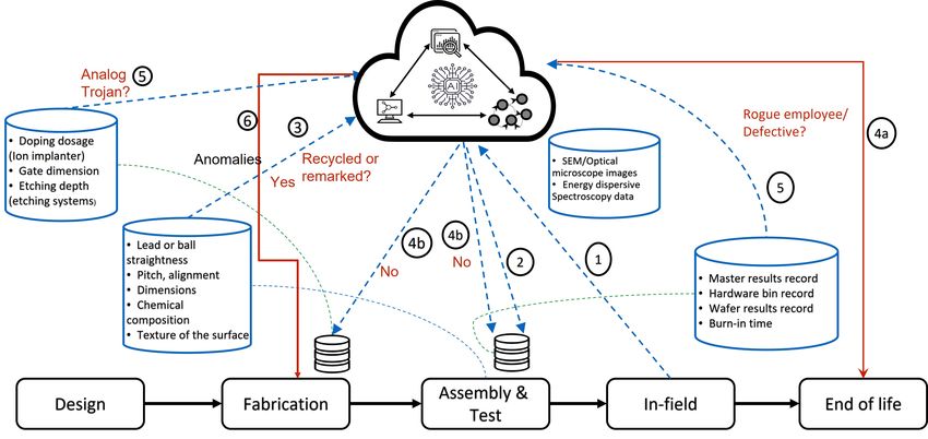
FUTURE HARDWARE SECURITY RESEARCH SERIES

                                                                       TABLE I
                      D IGITAL T WIN A PPLICATIONS S UGGESTED IN L ITERATURE FOR L IFECYCLE M ANAGEMENT AND C YBERSECURITY

  Paper                           Application Area                      Comments
  Bitton et al. [44]              Cybersecurity of Industrial Control   Proposed the use of DT to overcome the limitations of existing network
                                  Systems (ICS)                         penetration testing when applied to industrial SCADA systems
  Lou et al. [45]                 Cybersecurity of ICS                  Demonstrated the use of DT to address security issues of a refueling machine
  Balta et al. [46]               Process management                    Proposed a DT for anomaly detection and process monitoring of the fused
                                                                        deposition modelling AM process.
  Eckhart et al. [47]             Network and CPS security              Proposed a CPS twinning system where states of the physical systems are
                                                                        mirrored through the DT that can incorporate security enhancing features, such
                                                                        as intrusion detection.
  Saad et al. [48]                Network and grid security             Illustrated a DT’s capability in providing security against false data injection,
                                                                        Distributed-Denial-of-Service (DDoS) and network delay attacks in microgrids.
  Li et al. [49]                  Product lifecycle management          Proposed fault diagnosis and prognosis technique in aircraft wings through a
                                                                        dynamic Bayesian Network driven DT.
  Sleuters et al. [50]            System management                     Proposed a DT to capture the operational behavior of a distributed IoT system.
  Wang et al. [51]                Smart manufacturing                   Discussed how a DT may be used for intelligent semiconductor manufacturing.
  Jain et al. [52]                System management                     Proposed a DT to offer real time analysis and control of a photovoltaic system.
  Xu et al. [53]                  Process management                    Demonstrated a DT that offers real time diagnosis and predictive maintenance
                                                                        of a car-body side production line.
  Kaewunruen et al. [54]          Operational lifecycle management      Proposed a DT for sustainable management of railway turnout systems.
  Heterogeneous Integration       Reliability management for Semi-      Briefly discussed possible DT prospects for reliability management of semi-
  Roadmap 2021 Ed. [55]           conductor                             conductor devices.
  Alves et al. [56]               System management                     Developed a DT to monitor and control water management in agricultural farms
  Tchana et al. [56]              Operational lifecycle management      Developed a DT to address operational issues in linear construction sector.

B. Digital Twin for Lifecycle Management and Cybersecurity                   from fabrication and packaging processes. Another discussion
                                                                             of digital twins in context of the semiconductor fabrica-
   Fault diagnosis or root cause analysis as a core functionality            tion process can be found in [51]. Again, this discussion
of digital twins in context of product lifecycle management                  is limited to only one phase of the lifecycle in context of
and industrial production has been explored in several works                 smart manufacturing and not related to security concerns. The
[50], [52], [53]. DTs have been demonstrated to be applicable                current dominant trend in academia, which is evident in this
for lifecycle management in agricultural [56] and Building                   brief literature review section as well, is to utilize digital
Information Modelling (BIM) systems [57]. The existing lit-                  twin for systems which are almost exclusively manufacturing
erature on DT for cybersecurity focuses mainly on network                    systems or processes. We buck that trend in our paper by
and software security [58]. The focus has been on identifying                showcasing how digital twins can contribute significantly in
intrusion [47] or false data injection attacks in an industrial              secure lifecycle management as well.
setting. Bitton et al. proposed the use of a DT specified                       An overview of the papers discussed in the preceding can
automatically from a rule set derived from tests and a so                    be found in Table I.
called problem builder derived the constraints by solving a
non-linear maximization problem [44]. In a similar setting                   C. Hardware Security and Trust
of an ICS, DT has been used to resolve security issues                          Over past several decades, hardware of a computer system
associated with a refueling machine [45]. Saad et al. addressed              has traditionally been considered as the emphroot of trust to
attacks from potentially multiple coordinated sources on a                   guard against attacks on the software running on the system.
networked micro grid [48]. The reader should note that these                 The underlying assumption here is that since hardware is
approaches only consider specific type of control systems,                   less easily malleable than software, it is likely to be robust
not the security issues associated with the entire lifecycle.                and secure against different types of attacks [22]. However,
Lifecycle management of products, especially security man-                   emerging hardware attacks that exploit intralayer and cross-
agement, requires additional capabilities, considerations and                layer vulnerabilities have propelled hardware security as a
bidirectional transactions.                                                  widely researched topic. The recent proliferation of reported
   A high-level formulation of digital twins for semiconductor               attacks on hardware is not surprising given how the business
reliability can be found in [55]. Reliability concerns are                   model of the semiconductor industry has evolved over the
inherently limited to considering a subset of the lifecycle as               course of past few decades. Previously, all stages associated
vast majority of semiconductor reliability concerns originate                with bringing a semiconductor chip to the market (namely

                                                                         4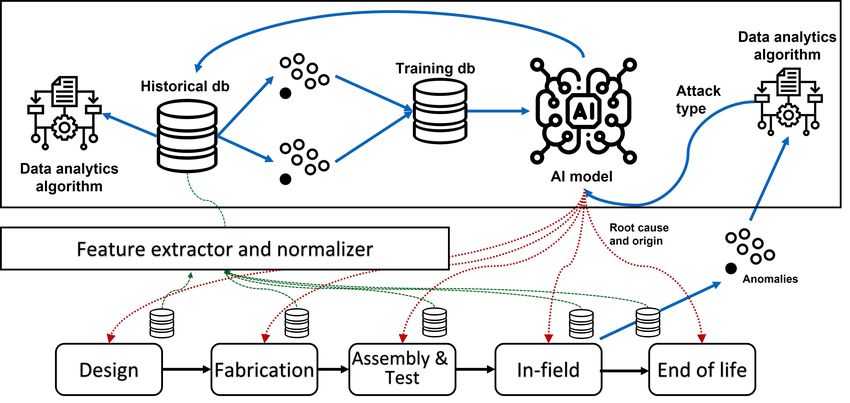
FUTURE HARDWARE SECURITY RESEARCH SERIES

design, fabrication, test, and debug) were handled by a single            lifecycle management in literature that attempt to provide
entity. To address aggressive time-to-market demands and                  security assurance to the lifecycle. In [40], authors present
profitability concerns, the global semiconductor industry has             their Synopsys SLM platform to assure quality, reliability,
gradually adopted a horizontal model of business wherein each             and security across the lifecycle. The proposed platform uses
previously mentioned stage may be handled by completely                   proprietary data engines to gain actionable insights to address
different entities often situated in different parts of the globe.        various design and manufacturing issues. Although authors
Several of the IPs used in a typical SoC are procured from                claim that the analytics engines can be used for bolstering
third-parties across the globe [59]. Today, most SoC design               security defenses, there is no clear guideline provided on
houses are “fabless,” meaning that they do not own a foundry              what data items are related to security vulnerabilities and
to physically fabricate the chips that they design. They rely on          how these relationships can be leveraged to defend against
a foundry and a third party to respectively fabricate and dis-            different types of security threats. Inspired by similar practices
tribute the chips for them. The consequence of this distributed           in software domain, the authors present a hardware secure
manufacturing and supply process is that the security of the              development lifecycle (HSDL) [69] composed of five phases
designed SoC may become compromised through malicious                     to identify and mitigate security issues as early as possible
modification by multiple entities across the entire supply chain.         in the lifecycle. However, the proposed approach is a general
This raises the issue of trust between multiple entities referred         pointer on what steps to follow for secure hardware devel-
to as hardware trust. Hardware attacks can take place in the              opment without specifics on how to achieve them through a
form of a malicious modification of circuit (hardware trojan),            singular framework. In [19], traceability for hardware trojans
stealing of the IP by the foundry, recycling and remarking of             is provided through a unified framework, however, it only does
chips, physical tampering [60], [61], reverse engineering [62],           so for a specific hardware threat vector.
[63], and side channel attacks by end users. These attacks
might be carried out by different actors in the supply chain                III. D IGITAL T WIN FOR S ECURING S EMICONDUCTOR
who may have different goals. In addition to these attacks,                L IFECYCLE M ANAGEMENT: P ROBLEM D EFINITION AND
various vulnerabilities might be introduced unintentionally in                            M OTIVATING E XAMPLES
the design, such as the leakage of a security critical asset                 In the hardware security domain, academia has proposed
through an output port or to an unauthorized IP. The possible             many different algorithms and testing methodologies to detect
hardware attacks and the stages in which they might occur                 different types of hardware attacks. Also, many proposals
are highlighted in red on the right side of Figure 2. These               called design for security (DfS) approaches have been inspired
attack vectors have highly varied associated threat models,               by established design for testing (DfT) practices, which advo-
characteristic symptoms, and detection methodologies.                     cate for embedding different sensors into a chip or leveraging
                                                                          data from existing chips to better prevent attacks. However,
D. Data-driven Approaches for Assuring Quality, Reliability,              the challenge is that the device is more likely to exhibit an
and Security in Semiconductor                                             anomalous behavior during its operation or when subjected
   The basic building blocks of a digital twin (i.e., data                to a test, thus it is up to the defender to understand why
collection and analytics) are already an indispensable part of            this behavior is occurring. As semiconductor industry has
existing flows in traditional semiconductor lifecycle; however,           gradually shifted from a vertically integrated business model
data driven approaches that leverage this sizeable amount of              to a globally distributed one, there can be multiple possible
data to manage the whole lifecycle have rarely been reported.             explanations for a single anomalous behavior as there are
Data obtained from these steps can be analyzed to provide                 many untrusted entities in the supply chain. Vast majority of
assurance to broadly three aspects of the semiconductor life-             existing literature on defense against hardware attacks have
cyle, namely quality, reliability, and security. As such, a digital       the underlying assumption that the attack vector is already
twin framework can be constructed to enhance each of these                known and detection or prevention methods against that attack
aspects without drastic modification of its existing design and           vector need to be developed. This assumption makes sense
process flows.                                                            if the threat model under consideration makes appropriate
   It should be noted that there is a fundamental difference              assumptions. In context of the whole lifecycle though, such
between product lifecycle management and security assurance               restrictive threat models do not apply. A naive solution might
through lifecycle management. While the former is concerned               be to put preventive measures in place on the chip to address
with satisfying the functional requirements of a product and              all possible attacks; however, as the sensors and circuitry
diagnosis of the underlying causes upon failure to do so,                 required are different, the performance penalty and hardware
the latter is concerned with preserving the desired security              overhead for doing so would be unacceptable.
properties of a system against attacks or unintentional mistakes             As a motivating example, let us consider three different
of the designer.                                                          scenarios. In the first two cases, the semiconductor device is
   In the last two decades, malicious modifications, vulnerabil-          a chip designed by a fabless design house.
ities, and attacks on hardware have been extensively reported                   a) Scenario 1: The design house receives customer
in literature and the press [64]–[68]. To the best of our                 feedback that a certain number of chips designed by them
knowledge, there have only been two approaches in the silicon             is experiencing accelerated aging. For the sake of focused

                                                                      5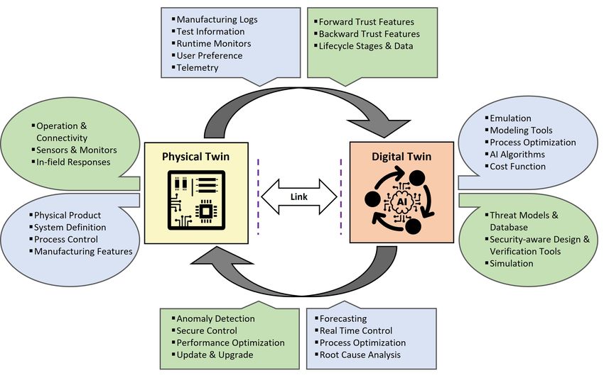
FUTURE HARDWARE SECURITY RESEARCH SERIES

Fig. 2. A high level overview of an AI driven DT framework adapted for security assurance in semiconductor lifecycle against various hardware attacks
(highlighted in red). The virtual environment is the cloud containing a digital representation of the design and lifecycle information of the physical semiconductor
device(s). The DT would be realized with a combination of computer modeling, data analytics and AI algorithms. To address challenges of hardware security
and trust, the DT would need to analyze the test, simulation/emulation, and sensor data uploaded to it throughout the lifecycle. With properly defined threat
models, the DT would not only infer the underlying attack vector, but also the lifecycle stage where it occurred. An iterative loop of data, control, and
reasoning will allow existing threat detection with precision (enabling backward trust) as well as provide insights for preventing emerging threats and zero-day
attacks (enabling the forward trust).

discussion on security assurance, let us also assume that the                           i. Designer overlooked the proper implementation of secu-
accelerated failure is not a reliability issue as the design                               rity policies while writing the hardware description code
passed through all reliability checks during the design phase.                             or even earlier at high level design specification stage.
In this scenario, the designers and the CAD tools used by the                          ii. A malicious information leaking hardware trojan was
design house are considered trusted. Now, the design house                                 introduced in the circuit in the design phase through
has to consider at least three possible explanations behind this                           3PIPs or inserted by the untrusted foundry.
behavior:                                                                               Given these two scenarios, backward trust functionality
   i. The failing chips are recycled or remarked chips that got                      of our proposed DT functionality will assign a probable
      resold as after they had reached their end of life.                            provenance to the observed anomalous behavior through root
  ii. The failing chips are out-of-spec or defective chips that                      cause analysis. Backward trust also entails identifying the
      should have failed the burn-in or wafer probe test during                      possible causes of an observed anomalous behavior in the first
      test and assembly. A rogue employee in the foundry or                          place. This functionality is illustrated in Figure 2 where the
      potentially the untrusted foundry itself is shipping some                      queries driving backward trust analysis are highlighted: what
      of the chips that failed these tests.                                          type of attack it is, where in the lifecycle it originated from and
 iii. The failing chips are infested with a process reliability                      who was responsible. The DT framework also will facilitate
      based trojan inserted by a rogue employee or the un-                           forward trust by ensuring that it is adaptable to future threats
      trusted foundry.                                                               insofar as their successful identification and application of root
                                                                                     cause analysis are concerned.
     b) Scenario 2: Infield testing such as JTAG testing and
Built-in-Self-Test (BIST) are often carried out after deploy-                          IV. S EMICONDUCTOR L IFECYCLE DATA FOR D IGITAL
ment to debug performance anomalies. In this scenario, let us                                          T WIN M APPING
assume that during such testing it is found that a confidential                        At the heart of every digital twin, there is bidirectional
asset such as a secret key can be observed through the                               data flow between the physical and virtual environments. Data
debug ports. Similar to scenario 1, there might be multiple                          can be exchanged either as it is collected or after preliminary
possible explanations each of which arise from either security                       analytics has been performed on it. As a semiconductor device
vulnerabilities introduced or attacks performed earlier in the                       moves through various phases of its lifespan, the tools and
lifecycle. We assume that the CAD tools can extensively verify                       software that are used to design it, the machinery that are
information leakage flows. The possible explanations for this                        used to manufacture it as well as the tests that are carried
behavior are as follows:                                                             out to ensure its proper operation generate a huge volume of

                                                                                 6
FUTURE HARDWARE SECURITY RESEARCH SERIES

data. The reader can consult Figure 3 to get a glance of the                  may describe the behavior and/or the structure of the
numerous steps a chip has to go through before it is ready                    circuit in a specialized language.
for use for in-field applications. The life of a semiconductor           c.   Functional verification: Next, the written RTL code
chip ends at the recycle facility. In between, the chip is                    is tested against the specification to verify whether it
fabricated by a foundry, assembled and tested and distributed                 has successfully captured the intended behavior and
to the market. Additional design features have to be added to                 functionality. The results of functional verification, also
each designed chip to reduce effort and complexity of testing                 known as logic simulation, are often stored in a Value
and debugging. These design for test (DfT) and design for                     Change Dump (VCD) file which contains information
debug (DfD) infrastructures are sometimes outsourced to third                 on the sequence of value changes in different signal
parties. Each of these stages of the lifecycle consists of several            variables with respect to time along with the file meta-
sub-phases; a high level overview showcasing every sub-phase                  data, definition of signal variables and timescale [86].
for the design, fabrication, test and assembly stages in Figure          d.   RTL to gate level synthesis: The RTL code is then
3.                                                                            synthesized to produce a schematic of the circuit in
   A discussion on DT for secure semiconductor lifecycle is                   terms of constituent logical gates. This process is entirely
impossible without an understanding of the lifecycle stages                   automated with help of commercially available tools.
and available data therein. Therefore, this section presents a                The synthesized netlist is a description of the nodes in
brief description of each of the lifecycle stages along with an               the circuit along with the interconnection between these
emphasis on the gathered data. At each stage of the lifecycle,                nodes.
industrial practice dictates the extensive collection and analysis       e.   DfT insertion: As mentioned previously, the complexity
of data to ensure reliability as well as satisfactory performance.            of modern VLSI circuits necessitates the inclusion of
Security is an afterthought in most cases although the rising                 additional features in the design for increased testability
threats in the global supply chain necessitate that the collected             of designs. DfT insertion step has similar outputs to RTL
data be used and analyzed for security assurance as well.                     to gate level synthesis step.
Academia has suggested various secondary analysis on the                 f.   Formal equivalence check: The design is verified by
available data that may be used for that purpose. For a detailed              formal assertions in the form of logical and mathematical
reference to how the collected data may be used to perform                    properties at this step. It provides a mathematical proof of
security assurance evaluations, the reader is advised to consult              functional equivalence between the intended design and
section V-B.                                                                  the synthesized netlist. At the end of the verification, the
                                                                              designer is informed of the no. of points in the design
A. Pre-silicon Design Stage                                                   that are equivalent to the intended functionality of the
                                                                              design.
   In the design phase of a semiconductor chip, a blueprint              g.   Floorplanning & placement: Floorplanning refers to the
of the chip to be fabricated is prepared and delivered to                     organization of circuit blocks within small rectangular
the foundry in the form of a GDSII file [70]. The design                      spaces of the available space. The precise location of the
must satisfy all specifications and perform desirably under                   I/O pins, power and clock distributions are determined in
all operating conditions and constraints (in terms of power,                  the placement step.
area, timing etc.) of interest. The design phase itself can be           h.   Clock tree synthesis: Clock tree synthesis step ensures
further subdivided into multiple sub-phases, all of which form                the even distribution of the clock to all sequential ele-
a sequential flow starting from architecture specification and                ments in the design, satisfaction of all timing constraints
ending at tape-out [71]. Today, most of the following sub-                    as well as minimization of skew and latency by clock tree
phases in the process are automated using a combination of                    building and balancing.
commercially available and open source software.                         i.   Routing: In the routing step, the myriad of interconnects
 a. Architecture specification: At this phase, a high level                   that connect different cells with each other as well as the
    description of the circuit to be designed is prepared taking              individual gates within each cell get outlined.
    various trade-offs and customer feedback into consider-              j.   Power, timing and physical signoff: Physical signoff
    ation. Vast majority of circuits ship with a specification                involves the verification of the physical design performed
    sheet that has detailed data on intended functionality, user              in the last four steps against technology node defined
    guide on how to use the setup and use the hardware                        design rules. Timing and power signoff verifies the phys-
    debugging features, data on important electrical, physical                ical design against timing and power requirements. At the
    and architectural properties such as operating tempera-                   end of verification, the designer has detailed information
    ture, clock speed, memory size, interface protocols etc.                  on whether important circuit parameters such as hold
 b. Logic design: Hardware Description Languages (HDLs)                       and setup time, dynamic, static and leakage power, and
    such as Verilog, VHDL, SystemVerilog etc. are used to                     interconnect and pat delay meet design requirements.
    describe and capture the specifications determined in the            k.   Tape out: The verified design is then shipped out to the
    previous step. The code written at this stage also known                  foundry in the form of a GDSII file.
    as Register Transfer Level (RTL) code. The code itself

                                                                     7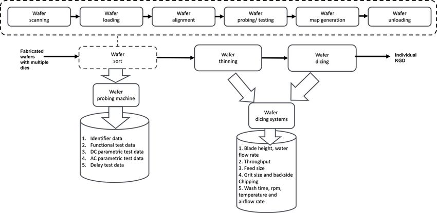
FUTURE HARDWARE SECURITY RESEARCH SERIES

8
    Fig. 3. A high-level overview of the first three stages of semiconductor lifecycle: Design, Fabrication, and Assembly & Test. The sub-stages represented with dashed line boxes indicate that they themselves
    can be dissolved into further sub-stages. In the fabrication stage, broadly the same processes are repeated to pattern different areas of the fabricated chip. This repetition of processes is denoted by a dashed
    line connecting the patterning process flow box with various sub-stages. The exact fabrication processes may vary depending upon the technology used by the foundry. The assembly and packaging process
    shown here is for Ball Grid Array (BGA) packages. For a different packaging technology (e.g., 3D and Quad Flat Packaging) the processes may be slightly different.
FUTURE HARDWARE SECURITY RESEARCH SERIES

                                                                        TABLE II
                                                             DATA AVAILABLE AT D ESIGN S TAGE

 Design sub-stage                Output Data files                Primary information/data                         Secondary analysis data
 Arch. Specification             Specification datasheet          Description of the intended functionality, op-   -
                                                                  erating limits, specific protocols and tech-
                                                                  nologies used
 Logic Design                    RTL                              Behavioral and/or structural description of      Branching probability, relative branching
                                                                  the circuit                                      probability [72], side channel leakage assess-
                                                                                                                   ment score [73]
 Functional verification         SAIF, VCD                        File metadata, timescale, variable type and      Coverage metrics [74], [75],
                                                                  bit-length, identifier codes
 RTL to gate level synthesis     Netlist, SDF                     List of nodes and their interconnections,        Controllability and observability of nets [76],
                                                                  delay information                                rare nets [77], [78]
 DfT insertion                   DfT inserted netlist, SDF        Same as RTL to gate level synthesis              Same as RTL to gate level synthesis
 Formal equivalence        and   Equivalency report               No. of primary outputs, and points in the        Test pattern generation for hardware trojan
 model checking                                                   circuit that are equivalent                      detection [79], secure information flow ver-
                                                                                                                   ified 3PIP cores [30], Code, functional and
                                                                                                                   toggle coverage [80]
 Floorplan and placement         Floorplan and placement db       Size and coordinates of the IO pads, IP          Chip temperature [81], power supply noise
                                                                  blocks and power network                         [82], overall electromagnetic radiation [83]
 Clock tree synthesis            Clock tree db                    Clock skew and latency                           Unused spaces in the layout [84]
 Routing                         Routed db (e.g., DEF ), post     Detailed location and geometry of intercon-      Wire length adjustments required for sup-
                                 place and route netlist          nects                                            pressing electromagnetic leakage [83]
 Parasitic extraction            SPEF                             Parasitic resistance and capacitance of nets     -
                                                                  and interconnects
 Power, timing, and physical     Timing, power and physical       Static, dynamic and leakage power, delay         Path delay fingerprinting for hardware trojan
 signoff                         signoff reports                  information, setup and hold time, and no. of     detection [85]
                                                                  DRC and LVS violations.
 Tape out                        GDSII                            Binary representation of layout geometries       -

   As mentioned previously, automation effort in the design                       to be used on, and many more. The most important technique
process is achieved by the use of commercially available                          during the fabrication process is photolithography which refers
software. These software collect and analyze data at each                         to a process to transfer an etched pattern from a chromium or
step to optimize performance and reliability of the design.                       quartz plate- called a photomask- onto a silicon wafer using
The data available from each stage is often stored in the                         light or electromagnetic radiation [88].
form of different software file formats. In literature, various                      The middle box in Figure 3 shows sub-stages of an exam-
types of secondary analysis have been proposed which can be                       ple fabrication process [89], [90]. This section describes the
performed on each of these files to derive secondary data of                      CMOS VLSI fabrication process in brief and also provides
interest. For example, the RTL file describing the behavioral                     a summary of data collected from various equipment on the
specification of the circuit can be analyzed to get information                   manufacturing floor.
about branching probability, control flow graph (CFG), data                          1) Mask writing flow: The process of manufacturing pho-
flow graph (DFG) which in turn may be used for security and                       tomasks is known as mask writing. The goal of the mask
performance optimization purposes [72], [87].                                     writing process is to transform the GDSII file, which is a
   A summary of available data from these sub-stages of design                    binary file format, to a format which is understood by mask
phase can be found in Table II. The readers are advised to                        writing tools [91] as well as to break the complex shapes
note that this table is not exhaustive; particularly, the data file               present in the GDSII into simpler polygons. A data preparation
formats and available secondary data may change depending                         step starts the mask writing process by performing graphical
on the software being used and the type of analysis being                         operations such as using Boolean mask operations to derive
performed respectively.                                                           mask layers that were not part of the original input data. Next,
                                                                                  to facilitate printing of features that are much smaller than
B. Fabrication and Manufacturing Stage                                            what would be possible for a particular wavelength of incident
   CMOS fabrication is an extremely sophisticated process in                      light, the geometrical shapes that are present in the GDSII need
which the exact steps followed depends on a large variety of                      to be augmented by applying different resolution enhancement
factors including the technology node, the operating conditions                   techniques (RETs) such as: optical proximity error correction
that the chip is expected to experience, performance as well                      (OPC) for nearby features, phase shifting features, scattering
as cost considerations, the device or application in which it is                  bars etc.

                                                                              9
FUTURE HARDWARE SECURITY RESEARCH SERIES

   For verification and metrology, the masks contain barcodes             photoresist coating, developing and stripping. The etching
and mask IDs. The RET applied mask data along with these                  system carries out the etching of materials underlying the
additional data is then ‘fractured’ into simpler polygons that            photoresist in either dry or wet etching process. Etching rate,
can be handled by the mask writing tools. The consequence                 trench slope, gas flow rate are example of data that can be
of addition of all these data to the original design data is that         obtained from an etching system.
the fractured file size is often several times more than the                 The aforementioned data from these machinery is collected
original GDSII [92], [93]. The mask data then needs to be                 through built-in sensors. These are also known as in-line,
passed to a mask shop, typically outside the foundry, who                 online or in-situ data. In addition to in-situ data, foundries also
will manufacture these masks. Often instructions regarding                utilize a wide range of ex-situ tests to provide a stronger and
how and where to carry out these measurements are contained               more precise feedback of fabrication process parameters. Ex-
in a specific file, known as measurement setup file, which                situ tests, otherwise known as offline tests, are also generators
are loaded into the tools. Once this file has been created, the           of a large volume of data. Some example of offline tests are
masks are then physically fabricated using similar processes              as follows:
to those that are used in fabrication of the chip itself. For               •   C-V profiling: Through the application of a DC voltage,
the sake of brevity, the discussion of these processes are only                 the width of the space charge region in the junction area
presented once, later in this section. The manufactured masks                   of a MOSFET may be manipulated. Using this principle,
are extremely expensive costing up to millions of dollars. As                   the C-V profiling test can determine the type of the dopant
such, they are encased in a protective membrane called pellicle                 as well as measure the doping density.
to protect against erosion, dust particle adherence, and other              •   Four-point probe: A typical methodology for measuring
mechanical damage.                                                              semiconductor resistivity, linewidths and sheet resistance
   2) Physical fabrication: The polycrystalline Electron                        is the four-point probe method. It is most usually em-
Grade Silicon(EGS) is processed through an apparatus called                     ployed as an absolute measurement that does not rely on
crystal puller to create the silicon ingot which is then mechan-                calibrated standards. Four point probe tests can be used to
ically shaped to a closed disc shaped wafer [89]. These blank                   construct sheet resistance contour maps which in turn can
wafer preparation steps are shown in the top right corner of                    be used to infer the doping density profile of the wafer.
the middle box in Figure 3. Using the masks prepared in mask                •   Thermal wave imaging: The wafer is subjected to
writing flow and the blank wafers, the physical fabrication of                  periodic heating stimuli. In the vicinity of the surface, the
the circuit commences. Again, the reader should be advised                      heating stimuli produces minute volume changes. These
that the process flow that is presented in Figure 3 or 4 and                    are detected with a laser by measuring the change in
described in greater detail in this section is representative; not              reflectance of the incident or pump laser [95]. The test
exhaustive. For circuits which are fabricated using a different                 data is represented in the form of a contour map.
for example, silicon-on-insulator (SOI) technology, the precise             •   Microscopy: Scanning capacitance microscopes (SCMs)
steps may differ.                                                               or scanning spreading resistance microscopes (SSRMs)
   The blank wafer is first thermally oxidized to form a layer                  can be used to build a later doping profile of the sam-
of SiO2 on top of it. This process is known as oxidation. The                   ple [96], [97]. Atomic force microscopes (AFMs) and
oxidation step is carried out in oxidation ovens or furnaces                    transmission electron microscopes (TEMs) can capture
which can tightly control the temperature and gas flow rate at                  images up to nanometer resolution. These high resolution
which the oxidation reaction occurs. A real time monitoring of                  images can be used for a variety of purposes including
the oxide thickness and oxidation rate is also possible in mod-                 critical dimension control, topography analysis, electrical
ern systems [90]. Then, different regions in the circuit such                   potential measurement etc.
as active area, isolation, the gate, the p/n well, metal layers
and contacts are patterned using photolithography through a
                                                                          C. Post-silicon Packaging, Assembly and Test
series of chemical and mechanical process shown in Figure 4.
The dopant present in the source and drain areas is introduced               1) Wafer Test: After the end of BEOL in the wafers with
through the bombarding the wafer surface by accelerated ions.             multiple dies are loaded onto an automatic test equipment
   Deposition of metal and nitride layer on top of the wafer              (ATE) called wafer probe station. A wafer prober is a highly
happens through either physical or chemical vapor deposition.             sophisticated equipment that applies test patterns to check
In newer technology nodes, chemical vapor deposition (CVD)                whether a given die on a wafer meets functional and parametric
is used extensively to deposit nitride, oxide and even metal              requirements based on which a chip is either accepted or
layers [94]. The CVD systems, similar to oxide furnaces,                  rejected for packaging. The dies that are accepted and rejected
also provide the foundry with extensive real time data on the             together form a color coded wafer map which can be viewed
temperature, pressure, reactant flow rate, reaction time and              by an operator in a computer. The entire wafer sort process is
growth diagnostics. The spin speed, applied torque, developed             illustrated in Figure 5 along with the data obtained from these
resist thickness and uniformity data, baking temperature, de-             steps.
velopment time, spray pressure data are all available from                   The wafer probing test itself applies test patterns in response
the modern cluster equipment that can combinedly perform                  to which the following data is gathered [98]:

                                                                     10
FUTURE HARDWARE SECURITY RESEARCH SERIES
11
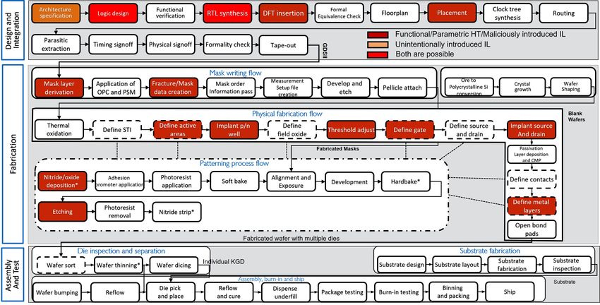
Fig. 4. Representative fabrication steps and data obtained therefrom. The colored dashed lines connecting equipment with steps indicate that the equipment is used for that step. On the other hand, the black
dashed lines around a box indicate that particular step contains many sub-steps which in turn are shown in the ‘patterning process flow” box. Many of the steps are carried out in the same equipment on
the foundry floor and therefore, generate the similar type of data. As the data is dependent on the particular tools being used, the exact list of data obtained may be different from what is shown, depending
on factors such as equipment vendors, process recipie, etc.FUTURE HARDWARE SECURITY RESEARCH SERIES
Fig. 5. Wafer testing process and possible data obtained. The dotted line around wafer sort signifies that it consists of sub-stages which are shown in the
dotted line rectangle at the top.
a. Functional test data: No. of stuck-at, transistor open and ogy (SMT), quad flat packaging (QFP), pin grid array (PGA)
short faults, the nets they occur in, fault and test coverage, and ball grid array (BGA) have been used. Recently, 2.5D and
no. of untestable of faults, automatic test pattern genera- 3D packaging technology have also been proposed. Depending
tion (ATPG) algorithm effectiveness. on the particular technologies being used, the steps followed
b. Electrical parametric test data: Various AC and DC in the packaging process would be different. Figure 3 shows
parameters such as output drive and short current, con- the steps for BGA packaging, more specifically flip chip BGA
tact resistance, input high and low voltages, terminal (FCBGA) packaging.
impedance and reactance.
c. Delay test data: The rise and fall times of transition, After the bond pads have been opened, a metal ’bump’ or
setup and hold times of sequential circuits are some of ball is deposited on top of these pads. This process is known
the data available from delay tests performed at wafer as bumping. These bumps will form the bond between the
test step. substrate of the PCB and the die when the dies are ’flipped’
d. Test identifier data: These data include device, lot and to be conjoined. The wafer is then diced and KGDs are
wafer ID, wafer flat position which is used for aligning, picked and placed by an automatic machine to its appropriate
no. of wafers discarded after wafer probing. place on the substrate ball side down. An epoxy type material
After the wafers have been probed, the dies that pass perfor- is deposited by capillary action underneath to fill the space
mance and functional requirements are sliced in wafer dicing between the balls and the package. This step is known as
systems. The data available from wafer dicing systems include underfilling. Underfill flow rate, chemical composition and
the blade rpm, wash time, temperature, water flow rate etc. are fluid temperature are some examples of the data available at
also shown in Figure 5. this stage.
2) Packaging and Assembly: Packaging refers to the pro-
cess of encapsulating the known good dies (KGDs) in pro- 3) Package and Burn-in Testing: Once the packaging and
tective insulating material and attaching metal balls or pins to assembly steps are completed, the fabricated ICs are subjected
them so that they can be accessed from the outside. Assembly to elaborate stress testing comprised of package and burn-in
refers to the process of binding all of these different ICs and testing to evaluate their longevity under real world operating
electronic components to a printed circuit board (PCB). Rapid conditions. Combined they are also sometimes known as
device scaling, growth in the number of I/O pins, necessity reliability tests. Preconditioning, temperature cycling, thermal
of access to DfT and DfD features, thermal, mechanical and shock, temperature-humidity accelerated stress testing form a
economic considerations has meant that packaging technology partial list of the series of stress tests that the chip is subjected
has continually evolved over the past 60 years. Through the to [99]. Some of the data items available from this series of
years, packaging technologies such as surface-mount technol- stress tests are shown in Figure 6.
12FUTURE HARDWARE SECURITY RESEARCH SERIES
Fig. 6. Data available from assembly, packaging and reliability test flows. The packaging flow shown is for Flip Chip Ball Grid Array (FCBGA) packaging
technology.
D. In-field Deployment Stage boundary scan description language (BSDL) specifica-
tion of existing JTAG features on a chip are provided by
On-chip performance, voltage, temperature monitors mon- vendors to customers. This ensures that customers can
itor relevant circuit and software parameters and collectively have a useful manual on what test features are present
form a report on the health and performance of the device. in their device and how to use them.
The availability of the tests listed in the following therefore, 3) Hardware Performance Counters (HPC): HPCs are spe-
depends largely on the on-chip sensors, DfT facilities, and the cial purpose registers provided in a chip that stores
interfacing software for a particular chip. Different vendors various performance related activities in the device.
also enhance the existing standards to offer additional debug- These statistics can usually be accessed by an operating
ging and testing features into their chip and as such, the data system (e.g., in Linux these may be accessed by the perf
available from these tests would largely depend on the specific instruction) or special purpose software for the purpose.
vendor and type of the chip. A list of data available from these tests may be found
1) Built-in Self Test (BIST): BIST is used to periodically in Table III.
test the circuit subsystems and their operation [100]. Its
V. E XISTING H ARDWARE ATTACK V ECTORS : DATA AND
main purpose is to verify whether different components
S ECURITY P ERSPECTIVES FOR DT
are working properly and in some cases, apply appro-
priate countermeasures. Two types of BIST are widely To keep our discussion focused, we describe three hardware
used: Logic (LBIST) and Memory (MBIST). LBIST security threats associated with the scenarios we mentioned
generates input patterns for internal scan chains using earlier in section III, namely: hardware trojans, counterfeits
a pseudo-random pattern generator such as linear feed- and information leakage. In this section, we also highlight the
back shift register.MBIST is used for detecting memory data items that have a correlation with these attack vectors.
defects and in some cases, repair those defects.
2) Joint Test Action Group (JTAG) debugging: JTAG is a A. Attack vectors
standard to access the boundary scan DfT features in a 1) Hardware Trojan (HT): A Hardware Trojan (HT) is a
chip to verify its functionality [101]. Although originally term that refers to a malicious alteration of a circuit. The
conceived as a means of overcoming limitations of bed- Trojan may take control of, alter, or obstruct the underlying
of-nails fixtures of testing PCBs after manufacturing, computing device’s components and communications. Trojan
today it is used for diagnosis of failing interconnects, trigger refers to the specific condition or the circuit that
memories, and testing functionality of ICs. Often a leads to the dormant trojan being activated. Trojan payload
13FUTURE HARDWARE SECURITY RESEARCH SERIES
14
Fig. 7. Example lifecycle substages where a hardware trojan inserted or information leakage vulnerability may be introduced unintentionally. Hardware trojan associated stages are marked in red whereas
information leakage stages are marked in orange. It should be noted that information leakage may be caused intentionally by both functional and parametric trojans. So, the red marked boxes may be
considered as source lifecyle stages of intentional information leakage.You can also read