THIN-FILM INGAAS METAMORPHIC BUFFER FOR TELECOM C-BAND INAS QUANTUM DOTS AND OPTICAL RESONATORS ON GAAS PLATFORM
←
→
Page content transcription
If your browser does not render page correctly, please read the page content below
Nanophotonics 2022; aop

Research Article

Robert Sittig*, Cornelius Nawrath, Sascha Kolatschek, Stephanie Bauer, Richard Schaber,
Jiasheng Huang, Ponraj Vijayan, Pascal Pruy, Simone Luca Portalupi, Michael Jetter and
Peter Michler

Thin-film InGaAs metamorphic buffer for telecom
C-band InAs quantum dots and optical resonators
on GaAs platform
https://doi.org/10.1515/nanoph-2021-0552 The presented advances in the epitaxial growth of QD/MMB
Received September 24, 2021; accepted January 25, 2022; structures form the basis for the fabrication of high-quality
published online February 8, 2022 telecom nonclassical light sources as a key component of
Abstract: The GaAs-based material system is well-known photonic quantum technologies.
for hosting InAs quantum dots (QDs) with outstanding Keywords: 1550 nm; metamorphic buffer; optical res-
optical properties, typically emitting at a wavelength of onators; quantum dots.
around 900 nm. The insertion of a metamorphic buffer
(MMB) can shift this emission to the technologically attrac-
tive telecom C-band range centered at 1550 nm. However,
 1 Introduction
the thickness of common MMB designs (>1 m) limits
 Semiconductor quantum dots (QDs) are an appealing
their compatibility with most photonic resonator types.
 choice for the role of nonclassical light source in quan-
Here, we report on the metal–organic vapor-phase epitaxy
 tum technologies. The combination of InAs QDs on GaAs
(MOVPE) growth of a novel InGaAs MMB with a nonlinear
 substrates has proven to be especially promising [1]. The
indium content grading profile designed to maximize plas-
 typical emission wavelength of this system lies around
tic relaxation within minimal layer thickness. This allows
 900 nm due to the compressive strain causing a signifi-
us to achieve the necessary transition of the lattice con-
 cant blue-shift, compared to the bulk emission of InAs.
stant and to provide a smooth surface for QD growth within
 However, long-distance quantum information applications
180 nm. Single-photon emission at 1550 nm from InAs QDs
 would highly profit from utilizing photons in the telecom
deposited on top of this thin-film MMB is demonstrated.
 C-band window (around 1550 nm), which allows low-loss
The strength of the new design is proven by integrating
 transmission through the atmosphere [2] and the glass fiber
it into a bullseye cavity via nano-structuring techniques.
 network [3]. There are two main approaches to reduce the
 blue-shifting strain on InAs QDs and obtain emission at
*Corresponding author: Robert Sittig, Institut für Halbleiteroptik und 1550 nm. The first is a change of the substrate from GaAs
Funktionelle Grenzflächen, Center for Integrated Quantum Science to InP [4, 5], and the second, the growth of a metamorphic
and Technology (IQST) and SCoPE, University of Stuttgart, Allman- buffer (MMB) below the QDs [6, 7]. Single-photon emission
dring 3, 70569 Stuttgart, Germany,
 from InAs QDs grown on InP has been studied extensively
E-mail: r.sittig@ihfg.uni-stuttgart.de. https://orcid.org/0000-0002-
8912-9008 for decades and significant advances have been reported
Cornelius Nawrath, Sascha Kolatschek, Stephanie Bauer, Richard in recent years [8, 9]. Nevertheless, from a device fabri-
Schaber, Jiasheng Huang, Ponraj Vijayan, Pascal Pruy, Simone Luca cation point of view, the MMB on GaAs approach offers
Portalupi, Michael Jetter and Peter Michler, Institut für Halbleiterop-
 distinct benefits: it avoids the introduction of phospho-
tik und Funktionelle Grenzflächen, Center for Integrated Quantum
Science and Technology (IQST) and SCoPE, University of Stuttgart, rous compounds into the structure and allows fine-tuning
Allmandring 3, 70569 Stuttgart, Germany. https://orcid.org/0000- the strain via the lattice constant of the matrix, providing
0003-3594-8558 (C. Nawrath). https://orcid.org/0000-0002-6078- more freedom for the QD growth parameters. Addition-
4818 (S. Kolatschek). https://orcid.org/0000-0003-3044-8693 ally, it unlocks access to efficient binary AlAs/GaAs dis-
(S. Bauer). https://orcid.org/0000-0002-3527-7275
 tributed Bragg reflectors (DBRs) as well as AlGaAs-based
(P. Vijayan). https://orcid.org/0000-0003-0012-4073
(S. L. Portalupi). https://orcid.org/0000-0002-1311-6550 (M. Jetter). etch-stop and sacrificial layers for various processing
https://orcid.org/0000-0002-2949-2462 (P. Michler) techniques.
 Open Access. © 2022 Robert Sittig et al., published by De Gruyter. This work is licensed under the Creative Commons Attribution 4.0 International
License.
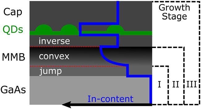
2 | R. Sittig et al.: Thin-film InGaAs metamorphic buffer for telecom C-band InAs quantum dots

 MMBs consisting of III-V materials are well-
established in a wide range of semiconductor devices,
such as high electron mobility transistors [10] and multi-
junction solar cells [11]. The functionality of these devices
is generally independent of the MMB thickness, provided
that a high crystalline quality is ensured. Therefore, MMBs
are typically at least 1 μm thick and their material com-
position is linearly or step-graded, because this approach
 Figure 1: Schematic structure of InAs QDs inside an InGaAs-matrix
facilitates control over properties like surface roughness lattice matched to an MMB grown on a GaAs substrate. The varying
and defect density [12]. indium content throughout the structure is illustrated in blue.
 Likewise, a linear InGaAs MMB with a thickness Growth optimization is performed in three consecutive growth
of 1080 nm enabled the first demonstration of single- stages I, II and III.
photon emission in the telecom C-band from InAs QDs
grown on the GaAs material platform [13]. Furthermore,
polarization-entanglement [14], on-demand generation of there is an upper limit for the possible mismatch, which is
entangled, single photon pairs [15] and indistinguishabil- given by the onset of 3D-growth as a competing mechanism
ity under continuous-wave (cw) two-photon-resonant [16] of strain energy reduction. Our proposed content grading
and pulsed resonant [17] excitation was shown by utilizing profile to provide the maximum possible strain energy at
the same design. However, this sample structure features any point, while staying within the limits of 2D-growth,
only a nominal 3 -cavity between bottom DBR and semi- is depicted by the InGaAs MMB in Figure 1. The grading
conductor/air interface. Employing an advanced photonic begins with an abrupt change (jump) of the indium con-
structure, e.g., a -cavity micro-pillar, would substantially tent, followed by a convex-up grading, and is completed by
improve the emission properties [18]. Therefore, enabling an inverse step. This jump-convex-inverse design is opti-
device fabrication is a crucial next step. mized in three successive growth stages named I, II and III.
 A suitable MMB design must fulfil three mandatory In stage I, which corresponds to only the jump-layer,
requirements. First, provide sufficient strain reduction to the aim is to induce a quick start of the plastic relaxation.
shift the QD emission to 1550 nm. Second, a smooth and Thus, we need to find the maximal permissible In content
homogeneous surface is a necessary prerequisite for all for this jump and the minimal thickness for the onset of
processing techniques. Third, in order to retain its compat- relaxation.
ibility with the AlAs/GaAs material system, the MMB must Once the lattice constant begins to increase, the
be placed inside the -cavity for most photonic structures. indium content can be increased further without gen-
This puts a strict upper limit on its thickness. Conse- erating 3D-structures. Following the same rationale, a
quently, the previous linear design is unsuitable for this convex-up function, in analogy to the metamorphic relax-
purpose and a thin-film replacement has to promote an ation curve [21], is deduced as the steepest possible grad-
extremely efficient transition of the lattice constant, while ing profile. This jump into convex-up design is compared
maintaining a high crystalline quality. with several alternatives in growth stage II. Additionally,
 the minimum thickness (i.e., maximum grading) that still
 maintains low surface roughness has to be determined.
2 Relaxation-optimized buffer Furthermore, in order to reach the desired lattice constant,
 design but avoid the stagnant saturation regime [22], an overshoot
 of In content is employed in the convex region before a
The intentional alteration of the lattice constant during decrease in the inverse region (see the dip at interface con-
metamorphic heteroepitaxy is achieved by inducing the vex/inverse). Notably, this overshoot has to be adjusted
formation of misfit dislocation segments into the pre- retroactively to enable a lattice-matched deposition of the
viously pseudomorphic layer. Thus, the strained layer fully relaxed inverse layer.
relaxes and adopts an in-plane lattice constant closer to its The main role of the inverse layer is to serve as a sub-
inherent value. Although the exact mechanisms respon- strate for the QD deposition and (together with the capping
sible for the formation of these segments are only partly layer) to provide the correct amount of strain release to
understood, this process is clearly driven by strain energy allow for the formation of InAs QDs with emission within
[19, 20]. Therefore, a large lattice mismatch with the sub- the telecom C-band. This will therefore be the pivotal
strate is desirable for the growth of a thin MMB. However, criterion for the optimization in stage III.
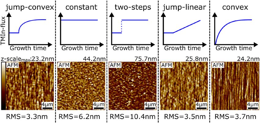
R. Sittig et al.: Thin-film InGaAs metamorphic buffer for telecom C-band InAs quantum dots | 3

 The key steps of the MMB growth calibration and Next, we reiterated the determination of the maximum
optimization are presented in the following. possible indium content, because a lower temperature
 is expected to suppress 3D-growth [25]. In contrast
 to the results at 710 ◦ C, no clear transition can be iden-
 tified, instead we observe an approximately linear relation
3 Optimization procedure between RMS and TMIn flux as shown in Figure 2C. How-
 ever, the surface topography for higher indium contents,
3.1 Jump layer optimization reveals ordering along the diagonal [001] and [010] direc-
 tions (see Supplementary). In contrast, metamorphic lay-
We adopted the starting parameters for the optimization
 ers typically exhibit a [011]/[01̄ 1] cross-hatch pattern [21].
of the jump-layer (stage I) from our default metal–organic
 Therefore, we decided to avoid this regime and adopted
vapor-phase epitaxy (MOVPE) growth of high quality GaAs,
 8.4 μmol/min as the maximum applicable TMIn flux for
namely a temperature of 710 ◦ C, a TMGa flux of 20.8
 the jump layer. This corresponds to an indium content of
μmol/min and an AsH3 flux of 2973 μmol/min. We then
 27.4 ± 0.2% according to XRD analysis.
grew samples with 50 nm thick layers of InGaAs by
 With the material composition and the temperature
adding varying amounts of TMIn into the mix. As shown
 defined, the next step was to find the minimum thick-
in Figure 2A, the RMS surface roughness of these lay-
 ness at which the layer starts to relax. For this purpose,
ers exhibits a sharp rise for TMIn fluxes greater than 7
 we grew samples with InGaAs layer thicknesses ranging
μmol/min, indicating a transition towards 3D growth. In
 from 20 nm to 400 nm and determined their respective
contrast, at 6 μmol/min we observe only a slight rough-
 relaxation via XRD. The results are displayed in Figure 2D.
ening compared to the baseline of 0.3 nm (GaAs grown
 The relaxation curve exhibits the typical behavior of meta-
in step-flow mode) while X-ray diffraction (XRD) analysis
 morphic growth, namely a steep increase after a certain
reveals metamorphic relaxation. We therefore selected this
 critical thickness, followed by saturation for thicker layers
value for further investigation.
 [22]. 30 nm is determined as the minimal thickness that
 The next step was to examine the influence of the
 exhibits a clear onset of relaxation (11.4%) and is therefore
growth temperature, as this parameter is crucial for con-
 used as parameter for the jump-step layer. This completes
trolling the diffusion of atoms on the surface and the
 the optimization of growth stage I.
mobility of dislocations inside the layer [23]. A corre-
sponding comparison of surface roughness is displayed
in Figure 2B. Increasing the temperature from 710 ◦ C to
 3.2 Convex grading layer optimization
750 ◦ C leads to significant roughening. On the other hand,
the RMS improves for lower temperature and only rises Figure 3 shows a comparison of our proposed jump-convex
again below 550 ◦ C, probably due to a general decline of content-grading profile with various alternatives, each
epitaxial quality caused by insufficient pyrolysis of the pre- reaching a maximum TMIn flux of 13.2 μmol/min within
cursors [24]. A growth temperature of 580 ◦ C is found to 200 nm. Using a constant or two-steps profile is clearly
be most advantageous, since it results in minimal surface inferior due to their higher surface roughness. Further-
roughness. more, employing a jump-linear or convex profile results

 Figure 2: Successive optimization steps of growth stage I. The red
 arrows mark the obtained parameter values.
 (A–C) RMS surface roughness of InGaAs layers with varying growth
 parameters. (A) Variation of TMIn flux for the growth of 50 nm InGaAs
 with 20.8 μmol/min TMGa flux and 2973 μmol/min AsH3 flux at
 710 ◦ C. (B) Temperature dependence of InGaAs with a TMIn flux of
 6.0 μmol/min. (C) Variation of TMIn flux at 580 ◦ C. (D) Strain relaxation
 of In0.274 GaAs depending on layer thickness.
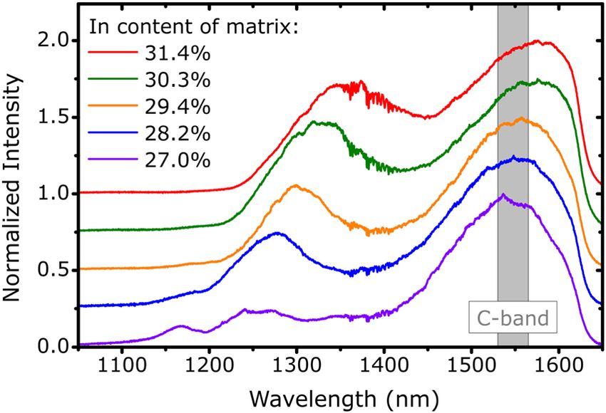
4 | R. Sittig et al.: Thin-film InGaAs metamorphic buffer for telecom C-band InAs quantum dots

 Figure 3: Optimization of growth stage II:
 Comparison between AFM-scans of various
 Inx Ga1−x As grading profiles to reach 13.2
 μmol/min TMIn flux. The constant section used
 in profiles 1, 3 and 4 has a thickness of 30 nm
 and the total thickness of each structure is
 200 nm.

in a similar RMS, but provides less average strain for the approximate geometrical length of a -cavity consisting
relaxation process. Therefore, we proceeded with finding of the deposited InGaAs [26]. A comparison between the
a suitable thickness for the grading layer. Notably, a thin- photoluminescence spectra of the five samples measured
ner convex segment steepens the necessary grading not under nonresonant excitation at 4 K is shown in Figure 4.
only directly, but also indirectly by decreasing the final Each spectrum is composed of two peaks. The peak around
relaxation, which entails a larger overshoot to reach the 1550 nm can be identified as QD emission and the one at
desired effective lattice constant. 130 nm was determined shorter wavelengths is assumed to stem from the wetting
as suitably thin, but still allowed adjusting the final indium layer or the InGaAs matrix. As expected, the higher the In
content without inducing 3D-growth (see Supplementary). content of the matrix, the stronger the red-shift of the emis-
This is necessary for the next task of simultaneously fine- sion. However, the QD emission peak maximum varies by
tuning the composition of convex and inverse/capping only 40 nm for the displayed composition range, compared
layer to obtain QD emission at 1550 nm in growth stage III. to the inhomogeneously broadened ensemble distribu-
 tions with a full width at half maximum (FWHM) of more
3.3 Inverse layer optimization than 150 nm. This means that the growth process is stable
 against small alterations of the indium content. Neverthe-
For this purpose, we fabricated five capped samples with less, microphotoluminescence ( -PL) measurements (not
the indium content inside the matrix around the QDs shown) revealed that the In0.294 GaAs configuration pro-
ranging between 27.0% and 31.4% (35.9% to 40.6% at duces the highest percentage of single QDs emitting in the
maximum of convex layer). The QDs were grown by deposit- 1545–1555 nm range. Hence, we selected this indium con-
ing InAs for 4 s with a TMIn-flux of 9.6 μmol/min at 595 ◦ C. tent as the most suitable, which finalized the optimization
The thickness of the inverse/capping layer was set to 60 of the jump-convex-inverse design.
nm/220 nm. This sets the QDs in the center of a structure
with a total thickness of 440 nm, which corresponds to the
 4 Photonic structures
 In order to illustrate the potential and quality of the novel
 MMB we fabricated two exemplary structures.
 The first one was grown on top of 23 AlAs/GaAs DBR
 pairs for increased light extraction and also features QDs
 with adjusted growth parameters to account for the depo-
 sition on the jump-convex-inverse MMB. The SEM scan
 in Figure 5A displays a side view of the two upper DBR
 pairs, the MMB and the capped QDs. The InGaAs structure
 is 450 nm thick in total, which corresponds to the mea-
 sured geometrical length for a -cavity as opposed to the
 approximated value used above. Notably, growth on AlAs
Figure 4: Optimization of growth stage III: Photoluminescence instead of GaAs had no adverse influence on the quality of
spectra of samples with varying indium content in the Inx Ga1−x As the MMB. The AFM scan in Figure 5B displays the surface
matrix around the QDs. The curves are offset vertically for clarity. topography of the sample. It is dominated by a cross-hatch
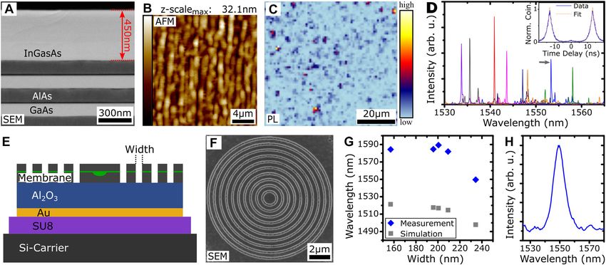
R. Sittig et al.: Thin-film InGaAs metamorphic buffer for telecom C-band InAs quantum dots | 5

Figure 5: Exemplary QD/MMB structures.
(A–D) Structural and optical investigation of a QD sample featuring an In0.294 GaAs-matrix and an AlAs/GaAs DBR. (A) SEM side view of the
two upper DBR-pairs, the jump-convex-inverse MMB and the capped QDs. (B) AFM scan showing the surface topography. The extracted RMS
is 4.68 nm. (C) -PL map. The color scale represents the emission intensity inside the C-band. An area density for the QDs of 3 × [106 ] cm−2
was extracted. (D) -PL spectra of eight exemplary QDs emitting inside the telecom C-band. The spectra are acquired under cw excitation
apart from the blue spectrum (marked with a grey arrow) for which the second-order auto-correlation measurement under pulsed conditions
(Inset) is acquired. (E–H) Bullseye structure for emission inside the telecom C-band. (E) Schematic of the sample after the flip-chip process.
An Al2 O3 spacer layer between the membrane and the backside gold mirror is used to enable constructive interference between the upwards
and the backreflected emission. (F) SEM top view of an exemplary processed circular Bragg grating cavity. (G) Simulated and measured
resonance wavelength of the fundamental cavity mode as a function of the trench width. (H) -PL spectrum of the cavity peak at 1550 nm
under high power above band-gap pumping.

pattern, which is typical for MMB structures [21], resulting is comparable as well (see below), the brightness of the
in an RMS of 4.68 nm. This topography remains homo- QDs in this sample structure can be estimated to ∼3% into
geneous over the whole sample. Figure 5C shows a -PL an NA of 0.6 [16] (see Supplementary). The mean value
map of the sample under cw nonresonant excitation in of the linewidth of the brightest transitions of a set of 26
which the color scale depicts the emission intensity inside exemplary QDs under saturation power (in cw excitation)
the telecom C-band. An analysis of distinct emitters allows is found to be 65.8 μeV (15.9 GHz) (FWHM) with a stan-
extracting an area density for optically active QDs of ∼3 dard deviation of 8.2 μeV (2.0 GHz). This is close to the
× [106 ] cm−2 , which signifies excellent conditions for the resolution limit of the spectrometer of ∼ 41 μeV (10 GHz).
excitation of isolated emitters, as required in quantum opti- A higher resolution is attainted by performing first-order
cal experiments. Furthermore, in contrast to the findings correlation measurements on a set of 17 different, exem-
reported in Ref. [13], the QDs are distributed uniformly plary QDs under the same excitation conditions yielding
with no visible preferred formation in specific areas of a mean value of 46.7 μeV (11.3 GHz) (FWHM) with a stan-
the cross-hatch. This indicates the absence of sufficiently dard deviation of 9.1 μeV (2.2 GHz) (see Supplementary).
strong strain fields on top of the relaxed inverse layer to The lineshape is dominated by Gaussian broadening. Both
influence the island formation [27]. A selection of exem- width and shape of the transition lines compare well to QDs
plary -PL spectra acquired under nonresonant excitation grown on a linearly graded MMB [16]. To gain insight into
is shown in Figure 5D exhibiting multiple sharp transi- the fine-structure splitting (FSS) of the QDs, polarization-
tion lines which is typical for QDs under this excitation resolved -PL measurements are performed on 26 QDs. The
scheme. QD emission can be found over the full range of mean value of the FSS is 23.4 μeV with a standard deviation
the C-band. Note that the measurements are taken under of 20.6 μeV, thus a reasonable number of QDs exhibit an
cw excitation except for the transition marked with the FSS below 10 μeV (see Supplementary). Note that this value
arrow (see figure caption). The intensity is comparable to is based in part on the polarization-dependent spectral
the sample investigated in Ref. [13]. Since the decay time shift of single transition lines, as a clear biexciton–exciton
6 | R. Sittig et al.: Thin-film InGaAs metamorphic buffer for telecom C-band InAs quantum dots

pair could only be identified in 6 out of 26 cases. The This can possibly be explained by the simplified and aver-
brightest transition line exhibits an FSS for 7 out of the aged refractive index used in the simulations. In contrast,
26 investigated QDs, suggesting the trion recombination to the real refractive index is highly dependent on the material
be favored, as was the case of the linearly graded MMBs [13, composition and temperature. Furthermore, a small varia-
28]. The QDs also compare well with respect to decay time tion of the membrane or Al2 O3 layer thickness can yield an
[13, 16, 17]. Time-correlated single-photon counting mea- additional small difference. An exemplary -PL spectrum
surements have been performed under weak, pulsed, non- of a cavity peak around 1550 nm (trench width of 240 nm)
resonant excitation for 13 exemplary QD transitions. The and a Q-factor of 160 (simulated Q-factor of 240) is dis-
decay traces are predominantly mono-exponential with a played in Figure 5H, thus demonstrating the feasibility of
mean decay time of 1.39 ns (standard deviation 0.16 ns). fabricating Bullseye cavities in the telecom C-band based
The nonclassical nature of the emitted light is demon- on the jump-convex-inverse MMB design. In the future, in
strated for an exemplary second-order auto-correlation order to achieve a perfect spatial overlap between a pre-
function g(2) ( ) under pulsed, nonresonant excitation and selected QD and the fundamental cavity mode, a determin-
displayed in the inset of Figure 5D. The measurement istic approach similar to Ref. [32] will be exploited as this
was acquired with a mean, total count rate of 76.9 kcps, can readily be transferred to the telecom wavelengths [33].
integrating for 45 min using superconducting nanowire
single-photon detectors with an efficiency of >80% and it
is displayed with a binning of 50 ps. The evaluation of the fit
 5 Conclusion and outlook
function (orange) yields g(2) (0) = 6.11(9)% including a cor-
 We realized the MOVPE growth of a thin-film InGaAs MMB
rection for dark counts of the detectors. Similar values have
 with a thickness as small as 180 nm on a GaAs substrate,
been determined for other QDs on this sample and only
 by optimizing a nonlinear grading profile designed for effi-
minor bunching is found on time scales of up to ±2.5 s.
 cient plastic relaxation. Furthermore, we demonstrated
 In sum, the QDs show comparably promising results
 that the strain on InAs QDs placed inside a respective
as their counterparts grown on a linearly graded MMB in
 InGaAs matrix can be adjusted to obtain telecom C-band
terms of brightness, linewidth and shape, FSS, decay time
 photons. The MMB/QD structure was subsequently grown
and single-photon purity.
 directly on a GaAs/AlAs DBR. This sample exhibits high
 The second investigated structure is a circular Bragg
 surface quality and allowed us to demonstrate single-
grating (bullseye) cavity realized via a flip-chip process.
 photon emission. Finally, the structure was integrated into
Such a cavity design has been demonstrated with QDs
 a Bullseye cavity to prove its compatibility with highly
emitting in the near-infrared spectral region [29, 30] and
 appealing photonic resonator designs. This progress in
recently also for QDs emitting in the telecom O-band [31].
 MMB growth unlocks numerous approaches for the fab-
The approach has proven appealing for the realization of
 rication of high quality single-photon sources at 1550 nm.
high brightness nonclassical light sources.
 By reducing the inverse/capping layer thickness to
20 nm/180 nm and utilizing an AlGaAs sacrificial layer, Supplementary Material
a 360 nm thick membrane can be produced. This allows
for sufficient confinement in the growth direction via total The online version of this article offers additional mate-
internal reflection. The complete layer structure is sketched rial: Experimental methods section, supplementary AFM-
in Figure 5E and the SEM image in Figure 5F shows a scans, description of further optimization steps, a mathe-
processed Bullseye structure after electron-beam lithog- matical expression of the convex-up grading function and
raphy and chemical dry etching. -PL measurements were exemplary reciprocal space maps. Furthermore, the mini-
performed to investigate the cavity mode, ensuring its uni- mum achievable MMB thickness and QD area density, as
form feeding by high power above band-gap pumping. well as the spectroscopic study regarding the linewidth,
The spectral position of the fundamental mode for dif- fine-structure splitting and decay time of the QDs are
ferent trench widths is plotted in Figure 5G. For smaller presented.
values, a saturation behavior of the resonance wavelength
is observed, while for increasing trench widths the cavity Author contribution: R.S. developed the design, grew the
mode starts to blue-shift. This trend is verified by finite- samples and performed the material analysis measure-
difference time-domain simulations. However, a small off- ments with the support of M.J. C.N., R.Sc. and P.P. per-
set between simulations and measurements is observed. formed the single QD experiments. S.K., S.B., J.H. and P.V.
R. Sittig et al.: Thin-film InGaAs metamorphic buffer for telecom C-band InAs quantum dots | 7

designed, realized and characterized the Bullseye cavities [11] S. P. Philipps, W. Guter, E. Welser, et al., ‘‘Present status in the
with the support of S.L.P. R.S., C.N. and S.K. wrote the development of III − V multi-junction solar cells,’’ in Next
manuscript with the support of S.L.P. M.J. and P.M. coor- Generation of Photovoltaics, Berlin, Springer, 2012, pp. 1 − 21.
 [12] S. Sorokin, G. Klimko, I. Sedova, et al., ‘‘Peculiarities of strain
dinated the project. All authors contributed to scientific
 relaxation in linearly graded Inx Ga1−x As/GaAs (001)
discussions. metamorphic buffer layers grown by molecular beam epitaxy,’’
Research funding: We gratefully acknowledge the fund- J. Cryst. Growth, vol. 455, pp. 83 − 89, 2016..
ing from the German Federal Ministry of Education and [13] M. Paul, F. Olbrich, J. Höschele, et al., ‘‘Single-photon
Research (BMBF) via the project Q.Link.X (No. 16KIS0862). emission at 1.55 μm from MOVPE-grown InAs quantum dots on
 InGaAs/GaAs metamorphic buffers,’’ Appl. Phys. Lett., vol. 111,
We further acknowledge the European Union’s Horizon
 no. 3, p. 033102, 2017..
2020 research and innovation program under Grant Agree- [14] F. Olbrich, J. Höschele, M. Müller, et al.,
ment No. 899814 (Qurope). Partial funds of this work were ‘‘Polarization-entangled photons from an InGaAs-based
provided by Projects No. EMPIR 17FUN06 SIQUST and No. quantum dot emitting in the telecom C-band,’’ Appl. Phys.
20FUN05 SEQUME. These projects have received funding Lett., vol. 111, no. 13, p. 133106, 2017..
from the EMPIR programme co-financed by the Participat- [15] K. D. Zeuner, K. D. Jöns, L. Schweickert, et al., ‘‘On-demand
 generation of entangled photon pairs in the telecom C-band
ing States and from the European Union’s Horizon 2020
 with InAs quantum dots,’’ ACS Photonics, vol. 8, no. 8,
research and innovation program. pp. 2337 − 2344, 2021..
Conflict of interest statement: The authors declare no [16] C. Nawrath, F. Olbrich, M. Paul, S. Portalupi, M. Jetter, and
competing interests. P. Michler, ‘‘Coherence and indistinguishability of highly pure
 single photons from non-resonantly and resonantly excited
 telecom C-band quantum dots,’’ Appl. Phys. Lett., vol. 115,
 no. 2, p. 023103, 2019..
References [17] C. Nawrath, H. Vural, J. Fischer, et al., ‘‘Resonance
 fluorescence of single In(Ga)As quantum dots emitting in the
 [1] P. Michler, Ed. Quantum Dots for Quantum Information telecom C-band,’’ Appl. Phys. Lett., vol. 118, no. 24, p. 244002,
 Technologies, vol. 237, Berlin, Springer, 2017. 2021..
 [2] S.-K. Liao, H.-L. Yong, C. Liu, et al., ‘‘Long-distance free-space [18] P. Senellart, G. Solomon, and A. White, ‘‘High-performance
 quantum key distribution in daylight towards inter-satellite semiconductor quantum-dot single-photon sources,’’ Nat.
 communication,’’ Nat. Photonics, vol. 11, no. 8, pp. 509 − 513, Nanotechnol., vol. 12, no. 11, p. 1026, 2017..
 2017.. [19] J. Matthews, S. Mader, and T. Light, ‘‘Accommodation of misfit
 [3] G. P. Agrawal, Fiber-Optic Communication Systems, vol. 222, across the interface between crystals of semiconducting
 New Jersey, John Wiley & Sons, 2012. elements or compounds,’’ J. Appl. Phys., vol. 41, no. 9,
 [4] K. Takemoto, Y. Sakuma, S. Hirose, T. Usuki, and N. Yokoyama, pp. 3800 − 3804, 1970..
 ‘‘Observation of exciton transition in 1.3 − 1.55 μm band from [20] T. Kujofsa, W. Yu, S. Cheruku, et al., ‘‘Plastic flow and
 single InAs/InP quantum dots in mesa structure,’’ Jpn. J. Appl. dislocation compensation in ZnSy Se1−y /GaAs (001)
 Phys., vol. 43, no. 3A, p. L349, 2004.. heterostructures,’’ J. Electron. Mater., vol. 41, no. 11,
 [5] J. Skiba-Szymanska, R. M. Stevenson, C. Varnava, et al., pp. 2993 − 3000, 2012..
 ‘‘Universal growth scheme for quantum dots with low [21] A. Andrews, J. Speck, A. Romanov, M. Bobeth, and W. Pompe,
 fine-structure splitting at various emission wavelengths,’’ ‘‘Modeling cross-hatch surface morphology in growing
 Phys. Rev. Appl., vol. 8, no. 1, p. 014013, 2017.. mismatched layers,’’ J. Appl. Phys., vol. 91, no. 4,
 [6] N. Ledentsov, V. Shchukin, T. Kettler, et al., ‘‘MBE-grown pp. 1933 − 1943, 2002..
 metamorphic lasers for applications at telecom wavelengths,’’ [22] B. Rodriguez and J. Millunchick, ‘‘The role of morphology in the
 J. Cryst. Growth, vol. 301, pp. 914 − 922, 2007.. relaxation of strain in InGaAs/GaAs,’’ J. Cryst. Growth, vol. 264,
 [7] E. Semenova, R. Hostein, G. Patriarche, et al., ‘‘Metamorphic no. 1, pp. 64 − 69, 2004.
 approach to single quantum dot emission at 1.55 μm on GaAs [23] T. Sasaki, H. Suzuki, A. Sai, et al., ‘‘Growth temperature
 substrate,’’ J. Appl. Phys., vol. 103, no. 10, p. 103533, 2008.. dependence of strain relaxation during InGaAs/GaAs (001)
 [8] T. Müller, J. Skiba-Szymanska, A. Krysa, et al., ‘‘A quantum heteroepitaxy,’’ J. Cryst. Growth, vol. 323, no. 1, pp. 13 − 16,
 light-emitting diode for the standard telecom window around 2011..
 1550 nm,’’ Nat. Commun., vol. 9, no. 1, pp. 1 − 6, 2018.. [24] S. DenBaars, B. Maa, P. Dapkus, A. Danner, and H. C. Lee,
 [9] M. Anderson, T. Müller, J. Skiba-Szymanska, et al., ‘‘Homogeneous and heterogeneous thermal decomposition
 ‘‘Gigahertz-clocked teleportation of time-bin qubits with a rates of trimethylgallium and arsine and their relevance to the
 quantum dot in the telecommunication C band,’’ Phys. Rev. growth of GaAs by MOCVD,’’ J. Cryst. Growth, vol. 77, nos 1-3,
 Appl., vol. 13, no. 5, p. 054052, 2020.. pp. 188 − 193, 1986..
[10] J. Ajayan, D. Nirmal, P. Mohankumar, et al., ‘‘GaAs metamor- [25] A. M. Ceschin and J. Massies, ‘‘Strain induced 2D − 3D growth
 phic high electron mobility transistors for future deep space- mode transition in molecular beam epitaxy of InxGa1t-xAs on
 biomedical-millitary and communication system applications: GaAs (001),’’ J. Cryst. Growth, vol. 114, no. 4, pp. 693 − 699,
 a review,’’ Microelectron. J., vol. 92, p. 104604, 2019.. 1991..
8 | R. Sittig et al.: Thin-film InGaAs metamorphic buffer for telecom C-band InAs quantum dots

[26] A. Goldberg Yu and N. Schmidt, Handbook Series on [31] S. Kolatschek, C. Nawrath, S. Bauer, et al., ‘‘Bright Purcell
 Semiconductor Parameters, vol. 2, M. E. Levinshtein, S. enhanced single-photon source in the telecom O-band based
 Rumyantsev, and M. Shur, Eds., Singapore, World Scientific on a quantum dot in a circular Bragg grating,’’ Nano Lett.,
 Publishing, 1999. vol. 21, no. 18, pp. 7740 − 7745, 2021..
[27] Q. Xie, A. Madhukar, P. Chen, and N. P. Kobayashi, ‘‘Vertically [32] S. Kolatschek, S. Hepp, M. Sartison, M. Jetter, P. Michler, and
 self-organized InAs quantum box islands on GaAs (100),’’ S. L. Portalupi, ‘‘Deterministic fabrication of circular Bragg
 Phys. Rev. Lett., vol. 75, no. 13, p. 2542, 1995.. gratings coupled to single quantum emitters via the
[28] C. Carmesin, F. Olbrich, T. Mehrtens, et al., ‘‘Structural and combination of in-situ optical lithography and electron-beam
 optical properties of InAs/(In)GaAs/GaAs quantum dots with lithography,’’ J. Appl. Phys., vol. 125, no. 4, p. 045701,
 single-photon emission in the telecom c-band up to 77 k,’’ 2019..
 Phys. Rev. B, vol. 98, p. 125407, 2018.. [33] M. Sartison, L. Engel, S. Kolatschek, et al., ‘‘Deterministic
[29] J. Liu, R. Su, Y. Wei, et al., ‘‘A solid-state source of strongly integration and optical characterization of telecom O-band
 entangled photon pairs with high brightness and quantum dots embedded into wet-chemically etched
 indistinguishability,’’ Nat. Nanotechnol., vol. 14, no. 6, Gaussian-shaped microlenses,’’ Appl. Phys. Lett., vol. 113,
 pp. 586 − 593, 2019.. no. 3, p. 032103, 2018..
[30] H. Wang, H. Hu, T.-H. Chung, et al., ‘‘On-demand
 semiconductor source of entangled photons which
 simultaneously has high fidelity, efficiency, and
 indistinguishability,’’ Phys. Rev. Lett., vol. 122, no. 11, Supplementary Material: The online version of this article offers sup-
 p. 113602, 2019.. plementary material (https://doi.org/10.1515/nanoph-2021-0552).
You can also read