Optimization of surface-mount-device light-emitting diode packaging: investigation of effects of component optical properties on light extraction ...
←
→
Page content transcription
If your browser does not render page correctly, please read the page content below
Optimization of surface-mount-device
                 light-emitting diode packaging:
                 investigation of effects of component
                 optical properties on light extraction
                 efficiency

                 Tomoaki Kashiwao
                 Mayu Hiura
                 Yee Yan Lim
                 Alireza Bahadori
                 Kenji Ikeda
                 Mikio Deguchi

Downloaded From: https://www.spiedigitallibrary.org/journals/Optical-Engineering on 19 Jun 2022
Terms of Use: https://www.spiedigitallibrary.org/terms-of-use
Optical Engineering 55(2), 025101 (February 2016)

                Optimization of surface-mount-device light-emitting diode
                packaging: investigation of effects of component optical
                properties on light extraction efficiency
                Tomoaki Kashiwao,a,b,* Mayu Hiura,a Yee Yan Lim,b Alireza Bahadori,b Kenji Ikeda,c and Mikio Deguchia
                a
                  National Institute of Technology, Niihama College, Department of Electronics and Control Engineering, 7-1 Yagumo-cho, Niihama,
                Ehime 792-8580, Japan
                b
                  Southern Cross University, School of Environment, Science and Engineering, P.O. Box 157, Lismore, New South Wales 2480, Australia
                c
                  Tokushima University, Graduate School of Institute of Technology and Science, 2-1 Minamijosanjima-cho, Tokushima 770-8506, Japan

                              Abstract. An investigation of the effects of the optical properties of surface-mount-device (SMD) light-emitting
                              diode (LED) (side-view and top-view LEDs) packaging (PKG) components on the light extraction efficiency ηPKG
                              using ray-tracing simulations is presented. In particular, it is found that the optical properties of the PKG resin and
                              the lead-frame (L/F) silver-plating significantly affect ηPKG . Thus, the effects of the surface reflection methods of
                              these components are investigated in order to optimize the optical design of the LED PKG. It is shown that there
                              exists peak extraction efficiency for each PKG, and the cavity angle formed by the cavity wall is important to
                              the optical design. In addition, the effect of phosphor present in the mold resin is examined using a Mie scat-
                              tering simulation. Finally, an SMD LED PKG optical design method is proposed on the basis of the simulation
                              results. © The Authors. Published by SPIE under a Creative Commons Attribution 3.0 Unported License. Distribution or reproduction of this work in
                              whole or in part requires full attribution of the original publication, including its DOI. [DOI: 10.1117/1.OE.55.2.025101]

                              Keywords: light-emitting diodes; surface-mount-device packaging; optical design; ray-tracing simulation.
                              Paper 151252 received Sep. 10, 2015; accepted for publication Dec. 28, 2015; published online Feb. 2, 2016.

                1 Introduction                                                                           In previous studies, we investigated the effect of the
                White surface-mount-device (SMD) light-emitting diodes                               optical properties of the components of an SMD LED on
                (LEDs), which are composed of a combination of a blue                                the device ηPKG using ray-tracing simulations.28,29 In this
                LED chip and phosphor, are being used for various elec-                              study, we focus on the optical properties of PKG resin
                tronic instruments, and many LED manufacturers and                                   and L/F silver-plating. The optical properties of these mate-
                researchers are engaging in intensive competition to further                         rials have a significant effect on the ηPKG of LED PKG. Here,
                enhance white SMD LED performance.1–3 Of course,                                     the effects of the PKG resin and L/F silver-plating reflection
                improvement of the LED chip output is an important factor                            methods in particular are investigated. Side-view (SV)
                in the further development of all LEDs. In addition, however,                        LEDs, which are used for liquid-crystal display (LCD) back-
                improvement of the LED packaging (PKG) light extraction                              lights, and top-view (TV) LEDs, which are used for general
                efficiency ηPKG is also important.4–7 The PKG performance                            purposes such as LED illumination, are considered in this
                is primarily determined by the structure8 and optical pro-                           study. Note that the SV PKG cavity is narrower and the
                perties of the PKG components. The optical properties of                             light reflection frequency is higher than those of a general
                PKG components are particularly important parameters as                              LED PKG. On the other hand, the TV PKG cavity wall func-
                regards LED product performance, because an electric                                 tions as a light reflector. Therefore, the reflection methods
                input loss of more than 10% is caused by the PKG.4 In                                dependent on the component surface conditions are impor-
                the case of white LEDs, the PKG is composed of various                               tant to the LED PKG design. In addition, the phosphor in
                component materials, primarily PKG resin (injection mold-                            the mold resin has a significant effect on the ηPKG .30–34 In
                ing resin), mold resin (silicone or epoxy)9–11 containing a                          this study, we investigate the relationship between the com-
                phosphor12–16 and a diffuser material, a lead frame (L/F),17,18                      ponent reflection methods (the PKG resin and the L/F silver-
                die-bonding paste,19,20 and bonding wire.21–23 Each compo-                           plating) and the ηPKG of the LED PKG using ray-tracing
                nent has been investigated intensively with regard to its per-                       simulations in order to confirm the possibility of optimizing
                formance in each area of the device. Further, ray-tracing                            this device. Moreover, a simulation considering the phosphor
                simulations based on the Monte-Carlo method have been                                contained in the mold resin is performed in order to inves-
                used for optical design in the early phase of LED product                            tigate the effect of this substance on the ηPKG . Finally,
                development.24–27 This approach plays an important role                              important points regarding the SMD PKG optical design
                in terms of both cost and time reduction. Note that the pro-                         method are presented, which are based on the simulation
                duction of an LED PKG prototype has a high cost and is time                          results.
                consuming, because a die is required.                                                    In Sec. 2, the ray-tracing simulation is explained and the
                                                                                                     definition of the ηPKG examined in this study is presented.
                                                                                                     In Sec. 3, the simulation conditions are explained and the
                *Address all correspondence to: Tomoaki Kashiwao, E-mail: kashiwao@ect.              simulation results are shown and discussed. Finally, Sec. 4
                 niihama-nct.ac.jp                                                                   concludes the paper.

                Optical Engineering                                                         025101-1                                                February 2016   •   Vol. 55(2)

Downloaded From: https://www.spiedigitallibrary.org/journals/Optical-Engineering on 19 Jun 2022
Terms of Use: https://www.spiedigitallibrary.org/terms-of-use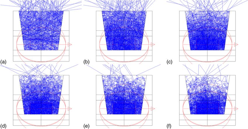
Kashiwao et al.: Optimization of surface-mount-device light-emitting diode packaging: investigation. . .

                2 Ray-Tracing Simulation                                                                                 2.2 Reflection Methods
                In this study, the LightTools 8.0.0, 8.1.0, and 8.2.0                                                    Mirror (specular), Gaussian, and Lambertian reflections are
                (Synopsys, Inc.) packages are used for the ray-tracing sim-                                              the reflection methods operating on the surfaces of the PKG
                ulations (Fig. 1). Numerous rays are emitted from the top                                                resin and L/F silver-plating of each PKG. The Gaussian
                surface of an LED chip in the top and bottom directions                                                  reflection angle is determined according to the Gaussian
                according to the simulated distributions. The rays undergo                                               function, with the mean being determined by considering
                repeated reflection and refraction several times in the LED                                              the angle of the mirror reflection and the standard deviation
                PKG cavity, and the intensities decrease according to the                                                σ, which represents the degree of scattering (mirror reflection
                reflection surface reflectance (Fresnel loss is ignored for                                              corresponds to σ ¼ 0 deg). Lambertian reflection corre-
                ray refraction in this study). Finally, the rays are emitted                                             sponds to complete scattering. Gaussian reflection at σ ¼ 0
                from the LED PKG. Thus, the optical properties of the                                                    to 30 deg in 1-deg increments and Lambertian reflection are
                PKG components significantly affect the PKG performance.                                                 the reflection methods considered in this study. The ηPKG of
                                                                                                                         each PKG is calculated for 1024 combinations of the PKG
                2.1 Light Extraction Efficiency                                                                          resin and L/F reflection methods in the simulations.
                ηPKG is used as an index to verify the LED PKG performance                                                  When rays are reflected from the cavity wall surface and
                and is defined as                                                                                        L/F, the relative intensity can be expressed as
                         P
                            I                                                                                                                                I n ¼ ρI n ;                             (2)
                ηPKG ¼ Pn Pn ;                                         (1)
                                                                                                                         EQ-TARGET;temp:intralink-;e002;326;572

                           I Cn
                EQ-TARGET;temp:intralink-;e001;63;568

                                                        n                                                                where I n is the relative intensity before emission from the
                                                                                                                         PKG and ρ is the reflectance of the reflection surface.
                where I Pn and I Cn are the relative intensities emitted from the
                                                                                                                         Thus, higher reflectance is both preferable and important
                PKG and LED chip, respectively, n ¼ 1; : : : ; N is the ray
                                                                                                                         in each case. In addition, the greater the number of repeat
                number, and N is the number of rays. (The ηPKG calculation
                is based on the total radiant flux, measured in Watt.) Thus,                                             reflections in the cavity, the smaller the eventual ηPKG .
                the PKG ηPKG means the ratio of the total relative intensity                                             Consequently, the PKG optical design should aim to reduce
                that is not absorbed by the LED PKG. As noted above, the                                                 reflection repetition in the cavity.
                ηPKG values of SV and TV PKG, such as those shown in                                                         In the ray-tracing simulation, actual scattering on the sur-
                Fig. 2, are investigated in this study.                                                                  face of the PKG resin and the L/F silver-plating can be mod-
                                                                                                                         eled as Gaussian reflection for σ ¼ 30 deg and over and
                                                                                                                         σ ≈ 15 deg, respectively, according to comparisons between
                                                                                                                         the simulation and actual experimental results. However, the
                                                                                                                         surface conditions are affected by the surface processing
                                                                                                                         methods and materials. For example, the PKG resin reflec-
                                                                                                                         tion method and reflectance are affected by the surface
                                                                                                                         processing conditions of the resin die, its materials (e.g.,
                                                                                                                         polyamide is generally used), and its components (e.g.,
                                                                                                                         the percentage of titanium oxide). In addition, the silver-
                                                                                                                         plating reflection method is close to mirror reflection and
                                                                                                                         its reflectance is higher than that of general materials; how-
                                                                                                                         ever, these characteristics are significantly affected by the
                                                                                                                         electroplating method. Therefore, the choice of PKG compo-
                                                                                                                         nents significantly affects the optical performance of the
                                                        Fig. 1 LightTools ray-tracing simulation image.                  LED PKG.

                                                                 Fig. 2 PKG without mold resin (a) SV PKG, (b) TV PKG with round cavity, and (c) TV PKG with square
                                                                 cavity.

                Optical Engineering                                                                              025101-2                                                   February 2016   •   Vol. 55(2)

Downloaded From: https://www.spiedigitallibrary.org/journals/Optical-Engineering on 19 Jun 2022
Terms of Use: https://www.spiedigitallibrary.org/terms-of-use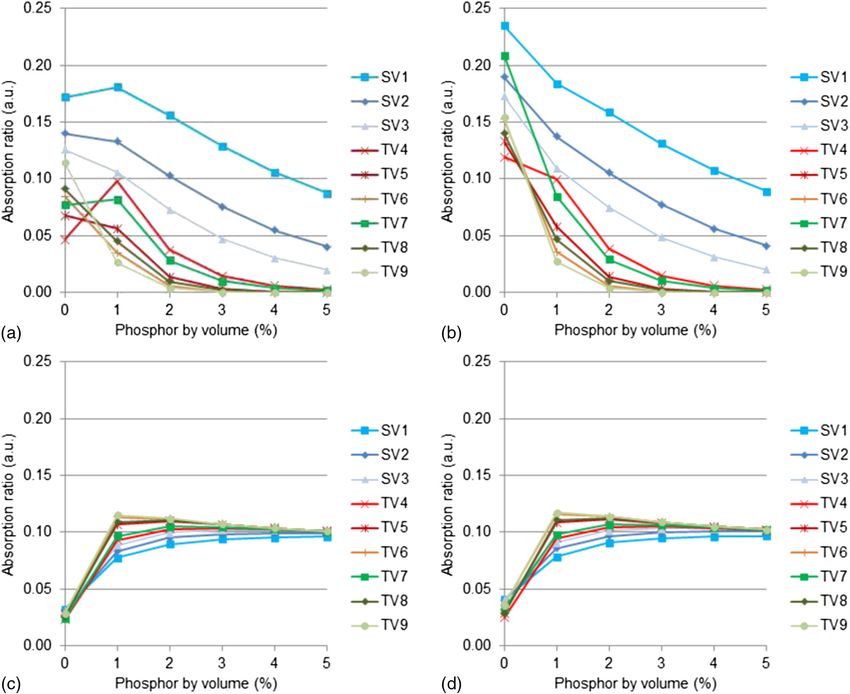
Kashiwao et al.: Optimization of surface-mount-device light-emitting diode packaging: investigation. . .

                                                                   Fig. 3 Dimensions of SMD LED PKG components.

                3 Simulation                                                                       hand, the TV PKG is used for general LEDs with a high out-
                                                                                                   put. Both types are still undergoing development and are
                3.1 Simulation Conditions                                                          being enhanced rapidly and intensively. Round- and square-
                Figure 3 shows the names and dimensions of the LED PKG                             shaped cavities are generally used. In this study, the optimal
                components, whereas Tables 1 and 2 show the simulation                             shape for TV PKG is confirmed.
                parameters. The SV PKG models are of three different sizes.                           Table 3 shows the common simulation conditions. The
                In addition, TV PKG models with three different round-                             optical properties were obtained from the widely used values
                cavity bottom diameters and three different square-cavity                          for these materials. The LED chip was modeled as a cuboid
                side bottom lengths are investigated. Both PKG types are                           sapphire with a refractive index of 1.78. The refractive index
                already internationally widespread. As noted above, SV                             of sapphire depends on the wavelength of the incident light,
                PKG is used for LCD backlights in electrical appliances,                           and it is ∼1.78 for the wavelength of the blue light emitted
                such as smart phones. Thus, the SV LED has a thin PKG                              from the LED chip. In practice, the structure of the LED chip
                (
Kashiwao et al.: Optimization of surface-mount-device light-emitting diode packaging: investigation. . .
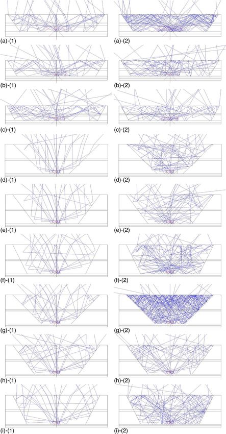
Fig. 5 ηPKG distributions for various PKG and L/F combinations (arbitrary unit: a.u.). The vertical and
horizontal axes are the σ of the PKG resin and L/F silver-plating, respectively: (a) SV1, (b) SV2,
(c) SV3, (d) TV4, (e) TV5, (f) TV6, (g) TV7, (h) TV8, and (i) TV9. σ > 30 deg corresponds to
Lambertian reflection.
Table 4 Maximum and minimum ηPKG values of each PKG.
Maximum value Minimum value
PKG ηPKG (a.u.) Resin: σ (deg) L/F:σ (deg) ηPKG (a.u.) Resin:σ (deg) L/F: σ (deg)
SV1 0.795 3 30 0.723 0 0
SV2 0.828 6 30 0.769 Lambertian 0
SV3 0.842 8 30 0.786 Lambertian 0
TV4 0.929 0 30 0.855 Lambertian 0
TV5 0.903 10 30 0.837 Lambertian 0
TV6 0.886 7 30 0.811 Lambertian 0
TV7 0.898 18 30 0.757 0 0
TV8 0.882 22 30 0.830 0 0
TV9 0.856 15 30 0.809 Lambertian 0
Optical Engineering 025101-4 February 2016 • Vol. 55(2)
Downloaded From: https://www.spiedigitallibrary.org/journals/Optical-Engineering on 19 Jun 2022
Terms of Use: https://www.spiedigitallibrary.org/terms-of-use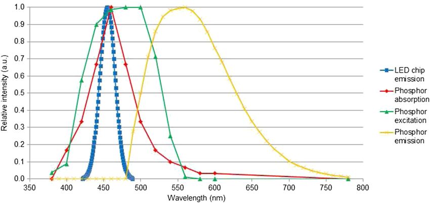
Kashiwao et al.: Optimization of surface-mount-device light-emitting diode packaging: investigation. . .

                                       Fig. 6 Ray-tracing simulation (20 rays): PKG resin and L/F combinations corresponding to maximum and
                                       minimum ηPKG values for each PKG. (a) SV1, (b) SV2, (c) SV3, (d) TV4, (e) TV5, (f) TV6, (g) TV7, (h) TV8,
                                       and (i) TV9. (1) and (2) represent maximum and minimum ηPKG values, respectively.

                Optical Engineering                                                        025101-5                                      February 2016   •   Vol. 55(2)

Downloaded From: https://www.spiedigitallibrary.org/journals/Optical-Engineering on 19 Jun 2022
Terms of Use: https://www.spiedigitallibrary.org/terms-of-use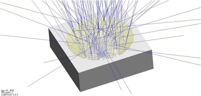
Kashiwao et al.: Optimization of surface-mount-device light-emitting diode packaging: investigation. . .

                significantly affects the device ηPKG because of the absorp-                      angle can be considered to be of the appropriate degree,
                tion in its P-GaN, InGan active, N-GaN, and electrode layers.                     because it yields the maximum value and the highest
                Moreover, there exist several types of blue LED chips,                            value of all the PKG when the PKG resin reflection is mir-
                namely, a horizontal, vertical (thin GaN chip), and flip                          ror-like. This suggests that the cavity wall functions as a light
                chip,35 and the emission efficiencies of these LED chips dif-                     reflector (Fig. 6). On the other hand, the SV PKG perfor-
                fer from each other. However, in this study, the ray emission                     mance is dependent on the PKG size, because of the narrow
                is set as a simple Lambertian distribution from the top sur-                      vertical direction of its PKG. However, when the results for
                face of the LED chip in the upward and downward direc-                            the round-cavity PKG are compared to those of the square-
                tions, ignoring the absorption and transmittance of the                           cavity PKG, the ηPKG of the round cavity is higher than that
                sapphire. This is done to facilitate easy extraction of the                       of the square cavity overall, despite the larger size of the
                effect of the PKG resin and L/F silver-plating surface con-                       latter. It can be observed that a number of the round-cavity
                ditions only on the ηPKG . In addition, the refractive index of                   reflections are smaller than those for the square-cavity case
                the mold resin is set to 1.43 in the simulation, because sil-                     in the ray-tracing simulation of Fig. 6. In the square-cavity
                icone may have refractive index values of roughly 1.4 to                          case, the angle of the plane surface toward the cavity center
                1.55; therefore, this value is not very well defined. If the                      point is inconsistent, and the rays are reflected between
                mold resin refractive index is increased, the critical angle                      the edges of the adjacent plane surfaces. However, this
                is decreased, and the rays are reflected from the light-emit-                     does not occur in the case of the round cavity. In addition,
                ting surface into the PKG cavity as a result of the total reflec-                 the extraction efficiencies of all the PKG are at maxima
                tion on the interface between the mold resin and the air.                         when the standard deviation of the L/F is at σ ¼ 30 deg
                Hence, ηPKG is decreased. Generally, the refractive index                         and at minima when the standard deviation of the L/F is
                of silicone is smaller than that of epoxy; therefore, silicone                    at σ ¼ 0 deg. Therefore, the reflection on the L/F should
                is chosen as the mold resin for LED PKG in which high effi-                       correspond to moderate scattering rather than mirror reflec-
                ciency is required. (The transmittance of the mold resin is                       tion. The total number of reflected rays in the PKG cavity
                ignored in this study.) Furthermore, the higher the reflectance                   decreases when the L/F surface reflection causes greater
                of the PKG resin and the L/F silver-plating, the higher the                       scattering, because the scattering tends to prevent total
                ηPKG (essentially). Thus, the reflectance performance of                          reflection on the PKG light-emitting surface. This can be rec-
                these materials, which we wish to enhance, is dependent                           ognized explicitly by comparing (1) and (2) of each PKG
                on their surface conditions, which are, in turn, determined                       in Fig. 6.
                by the fabrication processes. Generally, in the case of higher                        Figure 7 shows graphs of the ηPKG and absorption ratios
                values, the reflectance of polyamide containing titanium                          of the PKG resin and L/F for the conditions corresponding to
                oxide and the silver-plating products used for the LED                            maximum and minimum ηPKG values, respectively. The ηPKG
                PKG is roughly 90% to 95% and 95% to 97%, respectively;                           is higher if the absorption ratios of the PKG resin and L/F are
                however, these values differ widely among manufacturers in                        lower. In addition, greater ray absorption is exhibited by the
                accordance with the various types of technology employed in                       PKG resin in comparison to the L/F in all the simulation
                the fabrication processes.                                                        results. This means that the PKG performance is more sig-
                                                                                                  nificantly affected by the PKG resin optical design than that
                3.2 Simulation Results                                                            of the L/F.
                Figure 5 shows the simulation results. The ηPKG distributions
                of all the PKG exhibit mountain-shaped profiles. One peak                         3.3 Effect of a Phosphor
                and neighboring troughs can be observed in the distributions                      In the case of white LEDs, the mold resin contains yellow
                of each PKG (Table 4). It is preferable for the PKG resin                         phosphors to convert blue light emitted from the LED
                reflection to be close to mirror reflection. The TV4 cavity                       chip to white light. The LED emission efficiency is more

                                       Fig. 7 ηPKG values and absorption ratios of PKG resin and L/F under conditions corresponding to
                                       (a) maximum and (b) minimum ηPKG values for each PKG.

                Optical Engineering                                                        025101-6                                      February 2016   •   Vol. 55(2)

Downloaded From: https://www.spiedigitallibrary.org/journals/Optical-Engineering on 19 Jun 2022
Terms of Use: https://www.spiedigitallibrary.org/terms-of-use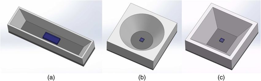
Kashiwao et al.: Optimization of surface-mount-device light-emitting diode packaging: investigation. . .

                                       Fig. 8 LED chip emission spectrum (blue) and phosphor absorption (red), excitation (green), and emis-
                                       sion (yellow) spectra. The emission spectrum is for all wavelengths of the excitation spectrum.

                significantly affected by the internal quantum efficiencies of                    difference in the energy between the absorbed and emitted
                the phosphors than the structures and optical properties of                       photons in the light wavelength conversion process.36
                the LED PKG components.30–34 There exists a down-conver-                          In addition, it is understood that the scattering caused by
                sion loss known as the “Stokes loss,” which is caused by the                      the phosphor contained within the mold resin affects the

                   Table 5 ηPKG of each PKG for combinations corresponding to maximum and minimum ηPKG values in simulation incorporating phosphor.

                                                                                              Percentage of phosphor by volume (%)

                PKG              Combination                  0                    1                  2                3                  4                      5

                SV1               Maximum                 0.79479             0.324044            0.170071          0.093153          0.052276              0.029689

                                   Minimum                0.72308             0.319442            0.166891          0.090814          0.050815              0.029062

                SV2               Maximum                 0.82816             0.310120            0.146984          0.072563          0.036873              0.019147

                                   Minimum                0.76912             0.300559            0.142330          0.070215          0.035718              0.018599

                SV3               Maximum                 0.84231             0.286228            0.121895          0.054349          0.024984              0.011830

                                   Minimum                0.78577             0.279097            0.118765          0.052834          0.024405              0.011573

                 TV4              Maximum                 0.92947             0.088049            0.012065          0.002009          0.000405              0.000137

                                   Minimum                0.85463             0.085842            0.011923          0.001949          0.000416              0.000127

                 TV5              Maximum                 0.90269             0.087252            0.012029          0.002024          0.000422              0.000144

                                   Minimum                0.83677             0.085419            0.011923          0.001968          0.000433              0.000136

                 TV6              Maximum                 0.88603             0.086201            0.012023          0.002041          0.000429              0.000147

                                   Minimum                0.81055             0.084842            0.011902          0.001983          0.000439              0.000141

                 TV7              Maximum                 0.89815             0.087950            0.012070          0.002017          0.000413              0.000139

                                   Minimum                0.75738             0.086884            0.011964          0.001967          0.000423              0.000133

                 TV8              Maximum                 0.88192             0.087351            0.012079          0.002034          0.000427              0.000147

                                   Minimum                0.83013             0.086476            0.011976          0.001988          0.000438              0.000141

                 TV9              Maximum                 0.85559             0.086735            0.012064          0.002052          0.000434              0.000150

                                   Minimum                0.80875             0.085547            0.011981          0.001990          0.000444              0.000143

                                                                                                                                                            (unit: a.u.)

                Optical Engineering                                                        025101-7                                     February 2016   •    Vol. 55(2)

Downloaded From: https://www.spiedigitallibrary.org/journals/Optical-Engineering on 19 Jun 2022
Terms of Use: https://www.spiedigitallibrary.org/terms-of-use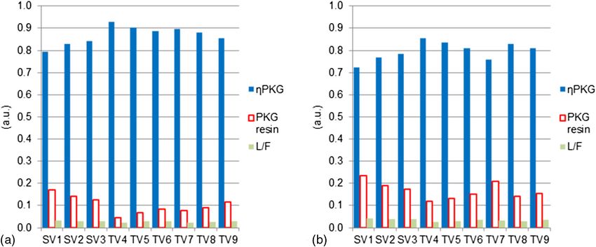
Kashiwao et al.: Optimization of surface-mount-device light-emitting diode packaging: investigation. . .

                ηPKG . Thus, in this study, we investigate the effect of the                      percentage by volume, the smaller the difference in the
                phosphors using a Mie scattering simulation performed                             extraction efficiency ηPKG between the maximum and mini-
                using LightTools 8.2.0, for a mold resin containing uni-                          mum conditions. In addition, if the phosphor percentage is
                formly distributed phosphor particles.36–38 In the simulation,                    increased, the absorption ratios of the PKG resin are
                the absorption, excitation, and emission spectrum distribu-                       decreased and those of the L/F are increased (Fig. 9).
                tions of the phosphor are set as default parameters in                            This is because the rays cannot reach the cavity wall (the
                LightTools 8.2.0. The phosphor particle radius is set to                          PKG resin) as a result of the scattering caused by the phos-
                1000 nm as the default setting. (The phosphor particle                            phors (Fig. 10). Thus, the L/F reflectance becomes more
                size is roughly 1 to 30 μm, in general.) These parameters                         important when the mold resin includes phosphors. In the
                are close to the properties of yttrium aluminum garnet:                           case of SV PKG, the rays can reach the cavity wall because
                cerium (YAG:Ce), which is generally used for white                                of the narrow cavity (Fig. 11). The absorption ratios of the
                LEDs based on a blue LED chip (Fig. 8). [The excitation                           SV1, TV4, and TV7 PKG at 1% phosphor by volume are
                (absorption) and emission spectra of YAG:Ce have peak                             higher than those at 0%, because the number of rays reflected
                wavelengths at ∼460 and in the range of 550 to 560 nm,                            in the cavity are increased by the scattering [Figs. 10(b) and
                respectively.] The spectrum distribution of the blue LED                          11(b)].
                chip is set as a Gaussian distribution (center wavelength:
                455 nm, full width at half maximum: 24 nm).38 (A blue
                LED chip with a peak wavelength of 450 to 470 nm is                               3.4 Discussion
                used for white LEDs.)
                                                                                                  From the simulation results, the following SMD PKG optical
                    The volume percentage of the phosphor in the mold resin
                                                                                                  design procedure can be proposed:
                is varied between 1% and 5% in 1% increments, and the ηPKG
                of the LED PKG for the PKG resin and L/F silver-plating                           Step 1-1: The largest possible cavity size should be
                combinations shown in Table 4 are verified. Table 5                                          designed in the case of SV PKG.
                shows the results of the simulation considering the phosphor.                     Step 1-2: A round rather than a square cavity should be
                Hence, it can be observed that the higher the phosphor                                      chosen in the case of TV PKG, if possible.

                                       Fig. 9 Absorption ratios for phosphor-containing mold resin: PKG resin under conditions corresponding
                                       to (a) maximum and (b) minimum ηPKG values. L/F under conditions corresponding to (c) maximum and
                                       (d) minimum ηPKG values.

                Optical Engineering                                                        025101-8                                     February 2016   •   Vol. 55(2)

Downloaded From: https://www.spiedigitallibrary.org/journals/Optical-Engineering on 19 Jun 2022
Terms of Use: https://www.spiedigitallibrary.org/terms-of-use
Kashiwao et al.: Optimization of surface-mount-device light-emitting diode packaging: investigation. . .
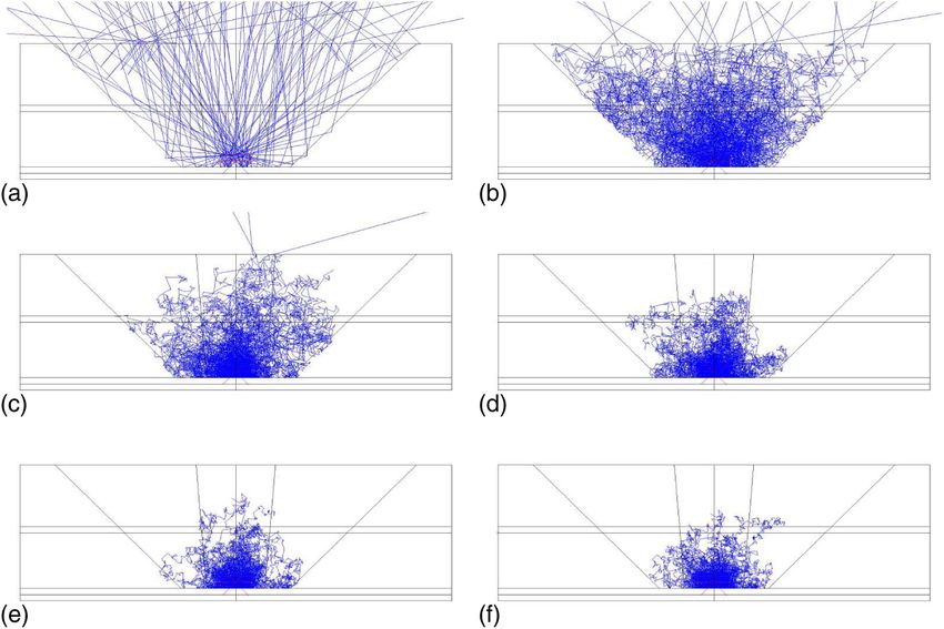
Fig. 10 Ray-tracing simulation (100 rays) of TV4 for phosphor-containing mold resin: (a) 0%, (b) 1%,
(c) 2%, (d) 3%, (e) 4%, and (f) 5% phosphor by volume.
Fig. 11 Ray-tracing simulation (100 rays) of SV1 for phosphor-containing mold resin: (a) 0%, (b) 1%,
(c) 2%, (d) 3%, (e) 4%, and (f) 5% phosphor by volume.
Step 2: The optimal cavity angle should be calculated using in reality. However, we can choose a combination of the
the ray-tracing simulation, considering the mirror PKG resin and L/F reflection methods that yield results as
reflection property of the PKG resin. close as possible to the peak of the ηPKG distribution, because
Step 3: It is preferable to have the PKG resin reflectance as the distribution exhibits a mountain shape with a single
close to mirror reflection as possible. peak (Fig. 5).
From the simulation results, it is preferable that the L/F
Designers and engineers must design LED PKG under silver-plating reflection exhibits proper scattering; however,
certain restrictions in order to satisfy specific target product the more the reflection is scattered, the lower the reflectance
requirements. Thus, the cavity angle should be designed to in actuality. Consequently, an investigation of the relation-
be as close as possible to mirror reflection in Step 2 above in ship between the silver-plating scattering profile and reflec-
cases where a cavity angle corresponding exactly to mirror tance using physical experiments is required. In the case
reflection is unrealistic. In addition, it is impossible to obtain where the mold resin includes a high phosphor content
complete mirror reflection using the examined components ratio, the effect of the optical properties of the PKG resin
Optical Engineering 025101-9 February 2016 • Vol. 55(2)
Downloaded From: https://www.spiedigitallibrary.org/journals/Optical-Engineering on 19 Jun 2022
Terms of Use: https://www.spiedigitallibrary.org/terms-of-useKashiwao et al.: Optimization of surface-mount-device light-emitting diode packaging: investigation. . .
is reduced; however, it is still apparent for a low phosphor 9. A. W. Norris, M. Bahadur, and M. Yoshitake, “Novel silicone materi-
als for LED packaging,” Proc. SPIE 5941, 594115 (2005).
ratio (Fig. 9). This is especially true for the SV PKG, which 10. M. Bahadur et al., “Silicone materials for LED packaging,” Proc. SPIE
has a narrow cavity. Moreover, the L/F silver-plating reflec- 6337, 63370F (2006).
11. X. Yang et al., “Preparation and performance of high refractive index
tance is more important in the presence of phosphor, because silicone resin-type materials for the packaging of light-emitting
the absorption caused by the L/F is increasing. diodes,” J. Appl. Polym. Sci. 127(3), 1717–1724 (2013).
12. S. Fujita et al., “YAG glass-ceramic phosphor for white LED (i): back-
ground and development,” Proc. SPIE 5941, 594111 (2005).
4 Conclusion 13. S. Tanabe et al., “YAG glass-ceramic phosphor for white LED (ii):
This paper reports on an investigation of the effects of the luminescence characteristics,” Proc. SPIE 5941, 594112 (2005).
14. S. Fujita, A. Sakamoto, and S. Tanabe, “Luminescence characteristics
PKG resin and L/F silver-plating surface reflection methods of YAG glass–ceramic phosphor for white LED,” IEEE J. Sel. Top.
on the ηPKG values of SVand TV LED PKG using ray-tracing Quantum Electron. 14(5), 1387–1391 (2008).
15. S. Fujita, Y. Umayahara, and S. Tanabe, “Influence of light scattering
simulations. From the simulation results, the ηPKG distribu- on luminous efficacy in Ce:YAG glass-ceramic phosphor,” J. Ceram.
tions of each PKG were found to exhibit mountain-shaped Soc. Jpn. 118(1374), 128–131 (2010).
profiles with a single peak, and this suggests a possibility 16. S. Nishiura et al., “Properties of transparent Ce:YAG ceramic phos-
phors for white LED,” Opt. Mater. 33(5), 688–691 (2011).
for optimization of SMD LED PKG. In addition, a larger 17. Z. Xu et al., “Reflection characteristics of displacement deposited Sn
SV PKG cavity was shown to be preferable, because of for LED lead frame,” Mater. Trans. 53(5), 946–950 (2012).
the narrowness of the cavity in the vertical direction. 18. Y. Yuan, H. Wang, and J. G. Liu, “An overview of light decay failure
modes in lead-frame LED packages,” in 11th China Int. Forum on
Moreover, the cavity angle is important as regards TV and Solid State Lighting (SSLCHINA), pp. 165–169, IEEE (2014).
SV PKG design, because the cavity wall functions as the 19. M. Kuramoto et al., “Die bonding for a nitride light-emitting diode by
low-temperature sintering of micrometer size silver particles,” IEEE
light reflector. If the maximum ηPKG of the TV PKG for mir- Trans. Compon. Packag. Technol. 33(4), 801–808 (2010).
ror reflection can be determined, the appropriate PKG cavity 20. M. Kuramoto et al., “New silver paste for die-attaching ceramic light-
angle can be obtained. In addition, a round-cavity PKG is emitting diode packages,” IEEE Trans. Compon. Packag. Manuf.
Technol. 1(5), 653–659 (2011).
preferable to a square-cavity device, because ray reflection 21. B. Wu et al., “Effect of gold wire bonding process on angular corre-
occurs between the adjacent walls in the square cavity. lated color temperature uniformity of white light-emitting diode,” Opt.
Furthermore, the optical design of the PKG resin was Express 19(24), 24115–24121 (2011).
22. H. H. Tsai et al., “An innovative annealing-twinned Ag-Au-Pd bond-
shown to be more important than that of the L/F silver-plat- ing wire for IC and LED packaging,” in 7th Int.Microsystems,
ing, based on the absorption ratio results. In addition, the Packaging, Assembly and Circuits Technology Conf., pp. 243–246,
IEEE (2012).
effect of the presence of phosphor on ηPKG was investigated. 23. J. Wu et al., “Bonding of Ag-alloy wire in LED packages,” in 35th
It was found that the importance of the PKG resin optical IEEE/CPMT Int. Electronic Manufacturing Technology Symp.,
properties decreases, whereas that of the L/F silver-plating pp. 1–4, IEEE (2012).
24. O. Shmatov, “Light extraction study of LED using ray tracing com-
reflectance increases for a mold resin containing phosphors. puter simulation,” Phys. Status Solidi (c) 4(5), 1629–1632 (2007).
Finally, an optical design method based on the experimental 25. N. Okada, “Optical simulation analysis for development of leading-
results was proposed. edge electronic device,” Toshiba Rev. 64(5), 34–37 (2009) (in
Japanese).
In future work, we will investigate the effect of the struc- 26. T. Kashiwao et al., “Development of a 2D optical simulator for SMD
ture and optical properties of the LED chip on the ηPKG . LED packaging,” J. Light Visual Environ. 38(0), 44–47 (2014).
27. T. Kashiwao, “A ray-tracing simulation technique for optical design of
Furthermore, the simulation results and the optical properties LED packaging,” Chem. Eng. 60(2), 101–110 (2015) (in Japanese).
of the components should be compared with measured 28. T. Kashiwao et al., “Effect of optical properties of construction ele-
results for actual LEDs and components in order to confirm ments for light extraction efficiency of SMD LEDs,” in Proc. of
SICE Annual Conf., pp. 1936–1940, SICE (2014).
the accuracy of the optical design based on the ray-tracing 29. M. Hiura et al., “Effect of optical properties of construction elements
simulation. for light extraction efficiency in side view LED packaging,” in Proc. of
Int. Symp. on Technology for Sustainability, National Taipei University
of Technology and National Institute of Technology of Japan (2014).
Acknowledgments 30. H. Luo et al., “Analysis of high-power packages for phosphor-based
white-light-emitting diodes,” Appl. Phys. Lett. 86(24), 243505 (2005).
This work was supported by the National Institute of 31. Z. Liu et al., “Optical analysis of phosphor’s location for high-power
Technology, Niihama College, Japan, and Southern Cross light-emitting diodes,” IEEE Trans. Device Mater. Reliab. 9(1), 65–73
University, Australia. We are grateful to Prof. Takao (2009).
32. N. T. Tran, J. P. You, and F. G. Shi, “Effect of phosphor particle size on
Shiomomura, Prof. Koichi Suzuki, and Prof. Scott T. luminous efficacy of phosphor-converted white LED,” J. Lightwave
Smith for their support. Technol. 27(22), 5145–5150 (2009).
33. C. Y. Chen et al., “High-efficiency white LED packaging with reduced
phosphor concentration,” IEEE Photonics Technol. Lett. 25(7), 694–
References 696 (2013).
34. C. C. Sun et al., “Packaging efficiency in phosphor-converted white
1. K. Bando et al., “Development of high-bright and pure-white LED LEDs and its impact to the limit of luminous efficacy,” J. Solid
lamps,” J. Light Visual Environ. 22(1), 2–5 (1998). State Light 1(1), 1–17 (2014).
2. I. Niki et al., “White LEDs for solid state lighting,” Proc. SPIE 5187, 1 35. O. Shchekin et al., “High performance thin-film flip-chip InGaN-GaN
(2004). light-emitting diodes,” Appl. Phys. Lett. 89(7), 071109 (2006).
3. Y. Narukawa et al., “Ultra-high efficiency white light emitting diodes,” 36. M. W. Zollers et al., “Process to measure particulate down-converting
Jpn. J. Appl. Phys. 45(10L), L1084 (2006). phosphors and create well-correlated software models of LED perfor-
4. K. Bando, “Performance of high-luminous efficacy white leds,” mance,” Proc. SPIE 7954, 795414 (2011).
J. Light Visual Environ. 35(3), 192–196 (2011). 37. M. Zollers, “Phosphor modeling in LightTools ensuring accurate white
5. N. T. Tran and F. G. Shi, “LED package design for high optical effi- LED models,” in LightTools White Paper, Synopsys, Inc. (2011).
ciency and low viewing angle,” in Microsystems, Packaging, Assembly 38. “Phosphor modeling in LightTools,” in Materials of LightTools
and Circuits Technology (IMPACT 2007). Int., pp. 10–13, IEEE Advanced Training, Synopsys, Inc. (2012).
(2007).
6. S. Liu and X. Luo, Led Packaging for Lighting Applications: Design,
Manufacturing, and Testing, John Wiley & Sons (Asia) Pte Ltd, Tomoaki Kashiwao has been an assistant professor at the National
Singapore (2011). Institute of Technology, Niihama College, Japan, since 2010 and
7. K. H. Kim et al., “Effects of the optical absorption of a LED chip on a visiting fellow at Southern Cross University, Australia, since 2015.
the LED package,” Solid-State Electron. 111, 166–170 (2015). He received his BE, ME, and DrEng degrees from Tokushima
8. H. Sun et al., “The model about the package structure of LED and University, Japan, in 2003, 2005, and 2009, respectively. In 2005,
the light intensity distribution,” Proc. SPIE 9276, 927610 (2014).
Optical Engineering 025101-10 February 2016 • Vol. 55(2)
Downloaded From: https://www.spiedigitallibrary.org/journals/Optical-Engineering on 19 Jun 2022
Terms of Use: https://www.spiedigitallibrary.org/terms-of-useKashiwao et al.: Optimization of surface-mount-device light-emitting diode packaging: investigation. . .
he joined the Nichia Corporation as an LED packaging design engi- Perth, WA, Australia. He is the author of several books published by
neer. His research interests include hybrid systems, LED packaging, multiple major publishers, including Elsevier, Springer, Taylor and
and neural networks. Francis, and John Wiley & Sons. He is a member of the Institution of
Engineers Australia and a member of the Australian Association for
Mayu Hiura has been a student of the advanced engineering course Engineering Education.
electronic engineering program, the National Institute of Technology
(NIT), Niihama College, Japan, since 2014. She received her asso- Kenji Ikeda has been an associate professor at Tokushima Univer-
ciate degree in engineering from NIT, Niihama College, in 2014. She sity, Japan, since 1994. He received his BE, ME, and PhD degrees
has studied the optical design of LED packaging. from the University of Tokyo, Japan, in 1986, 1988, and 1991, respec-
tively. His research interests include control engineering and system
Yee Yan Lim is currently a civil engineering lecturer in the School of identification.
Environment, Science, and Engineering, Southern Cross University,
Australia. He received his bachelor’s degree in civil engineering from Mikio Deguchi is a professor at the National Institute of Technology,
Nanyang Technological University, Singapore, in 2004, and his PhD Niihama College, Japan. He received his BE, ME, and DrEng degrees
from the same institution in 2012. His research interest is smart-mate- from Kyoto University, Japan, in 1983, 1985, and 2001, respectively.
rials-based structural health monitoring and energy harvesting. From 1985 to 1994, he was employed by the Mitsubishi Electric
Corporation and engaged in the development of high-performance
Alireza Bahadori is a lecturer and researcher with the School of manufacturing technology for silicon solar cells. His research interests
Environment, Science and Engineering at Southern Cross University, include semiconductor technology, plasma technology, electronic
Lismore, NSW, Australia. He received his PhD from Curtin University, circuits, and science education.
Optical Engineering 025101-11 February 2016 • Vol. 55(2)
Downloaded From: https://www.spiedigitallibrary.org/journals/Optical-Engineering on 19 Jun 2022
Terms of Use: https://www.spiedigitallibrary.org/terms-of-useYou can also read