Optical displacement metrology using alternating direction Moire
←
→
Page content transcription
If your browser does not render page correctly, please read the page content below

Optical displacement metrology using
                alternating direction Moire

                Kyoichi Suwa
                Koji Kaise
                Hiroki Tateno
                Nobutaka Magome

Downloaded From: https://www.spiedigitallibrary.org/journals/Optical-Engineering on 03 May 2020
Terms of Use: https://www.spiedigitallibrary.org/terms-of-use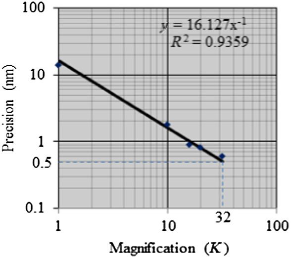
Optical Engineering 53(8), 084101 (August 2014)

                Optical displacement metrology using alternating
                direction Moire
                Kyoichi Suwa,a,* Koji Kaise,a Hiroki Tateno,a and Nobutaka Magomeb
                a
                 Nikon Corporation, Tokyo 100-8331, Japan
                b
                 Nikon Research Corporation of America, Belmont, California 94002, United States

                              Abstract. We develop a new double exposure Moire method for an optical registration metrology system in
                              photolithography. Our method enables us to achieve at least a factor of 10 improvements in precise displace-
                              ment metrology using a conventional optical sensor. We utilize a new registration mark printed to the photoresist
                              on a bare silicon wafer using a double exposure of the gratings. The mark consists of two types of Moire with
                              opposite phases. The two types of Moire are oriented in alternate directions. Displacement is measured from the
                              distance between the positions of the two types of Moire in analogy with the conventional registration method.
                              This concept is called alternating direction Moire. Performance is experimentally confirmed using an i-line wafer
                              exposure apparatus. Precision is improved by up to 32 times as compared with the conventional method and can
                              be applied to other Moire metrologies. © The Authors. Published by SPIE under a Creative Commons Attribution 3.0 Unported License.
                              Distribution or reproduction of this work in whole or in part requires full attribution of the original publication, including its DOI. [DOI: 10.1117/1.OE.53.8
                              .084101]

                              Keywords: semiconductor exposure apparatus; registration metrology; alternating direction Moire; double exposure; bar-in-bar
                              method; differential method; immersion ArF; error reduction.
                              Paper 140183 received Jan. 31, 2014; revised manuscript received Jun. 25, 2014; accepted for publication Jul. 8, 2014; published
                              online Aug. 5, 2014.

                1 Introduction                                                                           optical image magnification and sensor pixel size reduction.
                A wafer aligner is a semiconductor exposure apparatus that                               Other types of difficulties also arise when ensuring adequate
                aligns a wafer to a mask for each exposure field. Using a                                intensity to the solid state imaging pixels. In the conventional
                stage that sequentially moves field by field, the exposure appa-                         approach, reducing the measurement error involves moving
                ratus can expose a field with a series of alignment sequence                             the wafer stage very slowly and taking a large number of
                steps until the entire wafer surface is exposed. An optical                              data points, N. However,
                                                                                                                               pffiffiffiffi the reducing factor of the error
                registration metrology system (ORMS) measures the amount                                 is proportional to 1∕ N , and so an increasing N is time con-
                of exposure displacement error. Using some form of photoli-                              suming. An alternative approach to overlay measurements
                thography registration metrology, ORMS measurements are                                  employs scatterometry,4 which is used to reconstruct the
                possible during the alignment process using wafer alignment                              three-dimensional (3-D) shape of a registration mark from
                optics installed in the wafer aligner. Occasionally, these mea-                          diffracted light. Although this method has the potential to
                surements are done with an independent ORMS, which is                                    meet the requirements for registration metrology, lengthy
                a commercially available tool. Hereafter, we define ORMS                                 electromagnetic field calculations are required.
                to measure the photoresist marks on bare silicon wafers                                      In the field of optical measurements, the Moire effect is
                only. ORMS will then be used mainly for analysis of machine                              a well-studied phenomenon.5,6 The Moire method has a
                performance, which is very useful for wafer aligners.                                    particularly unique advantage in that it can significantly
                    The precision of the ORMS sensors has two limitations.                               improve the precision with no further demands on the sen-
                The first limitation relates to one-dimensional (1-D) laser                              sitivity of the optical sensor. For this reason, the Moire
                spot sensors.1 When a wafer must be moved beneath a fixed                                method is widely used for optical displacement measure-
                optical sensor,1 a scanning stage for providing object move-                             ments in optical encoders2,7,8 and curved surface metrol-
                ment is required for 1-D scanning optical sensors. The error                             ogy.9–12 We attempt here to implement Moire technologies
                in the position of the laser metrology system for stage mon-                             into ORMS in order to improve the measurement precision.
                itoring is generally larger than that of the optical sensor due                              There is much previous research in Moire, in particular
                to air temperature fluctuations and high frequency vibrations                            for measuring 3-D topology. However, in the context of
                of machine components,2 which are beyond the frequency                                   ORMS applications, our implementation to photolithogra-
                response of laser metrology, so the measurement precision                                phy belongs to 2-D Moire measurements, similar to that
                can never be small when using conventional metrological                                  found in optical encoders. With regard to an optical encorder,
                methods. The second limitation occurs when a two-dimen-                                  Ref. 8 has proposed an electrical signal process using two
                sional (2-D) imaging sensor is used to measure a motionless                              independent Moire fringe signals with the same phase.
                mark.3 It is difficult to improve the measurement precision in                           Many types of Moire measurements utilize a 2-D monitor
                this imaging mode due to the limits associated with the                                  camera to observe a real-time topological deformation.12,13
                                                                                                         Kafri has studied a double exposure technique5,11 in which
                                                                                                         the camera film realizes a Moire fringe image by exposing a
                *Address all correspondence to: Kyoichi Suwa, E-mail: kyoichi.Suwa@nikon                 shifted grating on a previously exposed grating as a reference
                 .com                                                                                    pattern.

                Optical Engineering                                                             084101-1                                                      August 2014      •   Vol. 53(8)

Downloaded From: https://www.spiedigitallibrary.org/journals/Optical-Engineering on 03 May 2020
Terms of Use: https://www.spiedigitallibrary.org/terms-of-use
Suwa et al.: Optical displacement metrology using alternating direction Moire
In registration metrology, measurement of the displace- Exposure light Reticle
ment between two points by photoresist images through dou- R2 R1
ble exposure is required. The photoresist image can indicate
problems in the exposure of a wafer aligner, such as regis-
tration error, machine vibration, and exposure stage error. Bar in bar
Such information is valuable because one can perform a cal-
ibration for the wafer aligner. The biggest advantage of using
Moire technology for ORMS is that the physical quantity to
be measured is highly magnified. For a double-exposed
Wafer
wafer, we measure the distance between two sequentially
exposed marks. The distance is magnified by the Moire phe-
nomena and calculated by dividing the Moire magnification
factor from the measured distance. In this case, theoretically,
Fig. 1 Double exposure to print bar-in-bar marks on the wafer using
the measurement error is not magnified. Therefore, the divi-
reticle 1 and reticle 2.
sion operation reduces the measurement error with the
inverse of the Moire magnification factor. As compared to
conventional approaches for reducing the error, our method
2.2 Alternating Direction Moire
does not require slow machine movements to record a large
number of data points. To implement Moire metrology into the bar-in-bar method
In Sec. 2, we describe our derived Moire method, called for ORMS, we develop a new concept using two types of
the alternating direction Moire (ADM). Applications to Moire, þθ and −θ, with opposite phases. Figure 2 shows
ORMS measurements are described in Sec. 3. From expo- the schematics of the general principle of ADM where the
sure experiments under i-line illumination, we verify the −θ Moire is assigned to A and A 0 , and the þθ Moire is
advantages of the ADM method in Sec. 4. In Sec. 5, future assigned to B. The Moire A and A 0 correspond to the two
applications to the most advanced immersion ArF tools and outside lines in the bar-in-bar system. Moire B corresponds
the possible merit of ADM are discussed. to the center line of the bar-in-bar system. As in the bar-in-
bar system, the offset term is cancelled by the differentiation
operation without loss of the precision as
2 ADM and ORMS
ORMS ≡ ½ðA − BÞ − ðB − A 0 Þ∕2: (2)
2.1 ORMS and Bar-in-Bar Method
This equation shows the displacement error between gratings
ORMS measurement precision is expressed by σ metrology.
G1 and G2 as shown in Fig. 2.
A first mark or set of marks is created on a wafer by a
It is notable that there is a large magnification factor
first exposure. A second mark or set of marks is created for the ADM in comparison to the bar-in-bar mark, which
by a second exposure. Assume that σ denotes the measure- strongly reduces the measurement errors.
ment precision of any one of the photoresist marks obtained
with metrology optics. Then, σ is the measurement error of
the sensor defined as the statistical error distribution from 3 Double Exposure ADM Method with
numerous data points, as described in the Appendix. Photoresist Mark
Assuming that a conventional ORMS measures the distance
between two marks, σ metrology is given by 3.1 Basic Concept in Practice
We propose the ADM method for ORMS. The first and the
pffiffiffi second exposures are initially performed for two different
σ metrology ¼ 2σ: (1) mask patterns consisting of arrays of lines. Resist develop-
ment leads to marks on the wafer with positions that are very
sensitive to stage alignment errors. Chromium lines on one
In our case, the marks are photoresist marks so that there is mask have an inclination angle, θ, with respect to the lines on
less waveform error for the optical signal. the other mask. The overlapped areas of the chromium lines
In conventional systems, the fundamental mark arrange- of the two masks lead to wedge-shaped unexposed areas on
ments for ORMS are the box-in-box14,15 or bar-in-bar.15 In the wafer, which emerge as a positive photoresist pattern
Fig. 1, the sequential process of the double exposure for the after development. The resulting set of unexposed patterns
bar-in-bar system is shown. In this process, two types of is in the form of a Moire pattern. Assuming the stage moves
reticles, R1 and R2, are used for the photomask. After the in the Y-direction in order to overlap the two patterns, the
reticle R1 is exposed on the wafer and the reticle R2 is resulting marks are displaced in the X-direction by an
also exposed with the stage in motion to make the bar-in- amount related to the inclination angle and the displacement.
bar pattern on the photoresist. In the case of the bar-in-bar In particular, a change in displacement DY causes a change
system, a line is exposed between the two previously exposed of DX ¼ DYð1∕ tan θÞ in the X-direction. The factor
lines. The relative position of the center line from the two (1∕ tan θ) is referred to as the Moire multiplication ratio.
outside lines corresponds to both the polarity of the direction This procedure is used to measure the distances between
and the amount of displacement. In this paper, we call this adjacent marks and then to divide the measured distances by
metrology method the differential method. This bar-in-bar the Moire multiplication ratio. It should be noted that all
system is also known as electrical micromeasurement.16 measurement errors are reduced by a factor of the Moire
Optical Engineering 084101-2 August 2014 • Vol. 53(8)
Downloaded From: https://www.spiedigitallibrary.org/journals/Optical-Engineering on 03 May 2020
Terms of Use: https://www.spiedigitallibrary.org/terms-of-useSuwa et al.: Optical displacement metrology using alternating direction Moire
Y A: -θ moire B:+θ moire A': -θ moire
P P +θ P
-θ -θ
∆Y
∆Y
∆Y
G1 G1 G1
∆X G2 G2 ∆X ∆X G2
X
Fig. 2 General principle of alternating direction Moire (ADM); the notation is different from that of chapter
3. The Moire pattern A observed when two grating images G1 and G2 are tilted with an angle −θ; if the
grating G1 is moved a distance Δy in the y -direction, the Moire pattern will move a distance
ΔX ¼ −ΔY ∕ tan θ in the x-direction. The Moire pattern B tilted with an angle þθ; if the grating G1 is
moved a distance Δy in the y-direction, the Moire pattern will move a distance ΔX ¼ ΔY ∕ tan θ in
the x -direction. Pattern A and pattern B have opposite phase. Pattern A 0 is identical to pattern A,
but the position is the opposite of pattern A.
Y
(a) (b) (c) (d)
X
Fig. 3 Combination of Moire photoresist patterns. (a) The first mask pattern. (b) The second mask
pattern. (c) Double exposed image. (d) Patterns after development used for ADM. There are seven
pairs of zigzag and straight lines.
multiplication ratio. In creating Moire photoresist images, the centerline of the zigzag pattern of the second mask pat-
the marks should meet the requirements for the ADM tern. The finite Δ case is shown in Fig. 5.
method, a zero point of the position should exist, and the
amount of its shift from the zero point should include direc-
tional information concerning the positional error. 3.2 Error Analysis of Measurements
Figure 3 shows how Moire photoresist images are created
We discuss the estimation of ADM measurement errors,
with the double exposure process. A Y-direction shift of the
where the following analysis is applicable to any type of
wafer, Δ, causes an X-direction shift of the mark, Λ. The
ORMS sensor. We analyze the ADM measurement error in
shift Δ is multiplied by the ratio, 1∕ tan θ, to create the latter
shift through the double exposure of a zigzag mark and ORMS, assuming measurement error follows a normalized
a straight line mark. θ is an angle between the zigzag and Gaussian distribution, hereafter called the normal distribu-
straight lines. At least three points of Moire photoresist tion in this paper, without loss of generality. The measure-
images are needed to meet the requirements for the ADM ment error is reduced by a factor equal to the inverse Moire
method. The changes in the coordinates of X1 to X2 and multiplication ratio. The coordinates of three Moire photo-
that of X2 to X3 are related to alignment errors through resist marks are given by
the Moire effect. Figure 4 shows the Moire photoresist
images when Δ is zero. The zigzag line in this figure is X1 ¼ −L þ Λ þ ε1 ; (3)
Y
Y
∆
Λ Λ Λ
L L
L L
X
X X1 X2 X3
X1 X2 X3
Fig. 5 Solid line represents the case where the Y -direction shift is Δ.
Fig. 4 Example of double exposed patterns. Dot-dashed line repre- X 1, X 2, and X 3 are the coordinates of the marks shifted by the multi-
sents the case where the Y -direction shift Δ is zero. plied shift, Λ.
Optical Engineering 084101-3 August 2014 • Vol. 53(8)
Downloaded From: https://www.spiedigitallibrary.org/journals/Optical-Engineering on 03 May 2020
Terms of Use: https://www.spiedigitallibrary.org/terms-of-useSuwa et al.: Optical displacement metrology using alternating direction Moire
X2 ¼ −Λ þ ε2 ; (4)
d
X3 ¼ L þ Λ þ ε3 ; (5)
LSA laser beam
Λ ¼ Δð1∕ tan θÞ: (6)
The measurement error of the detection for each mark is
written as εi . The physical quantity measured in this method
Λmeasured is defined as the difference between the distance of
X1 and X2 and that of X2 and X3, as depicted in Figs. 4
and 5.
Λmeasured can be expressed in terms of the true value Λ.
Λmeasured ¼ ½ðX3 − X2Þ∕2 − ðX2 − X1Þ∕2∕2
Fig. 6 Laser beam shaped into an elliptic spot. The short axis is about
¼ Λ þ ½ðε1 þ ε3 − 2ε2 Þ∕2∕2: (7) 4-μm long with a 40-μm long axis. Seven marks make up a row with
a pitch of d ¼ 4 μm.
Using Eqs. (6) and (7), Δ can be rewritten as
4 Experimental Results
Δmeasured ¼ tan θ½ðX3 − X2Þ∕4 − ðX2 − X1Þ∕4
4.1 Laser Step Alignment
¼ Δ þ tan θðε1 þ ε3 − 2ε2 Þ∕4 (8)
We focus our attention on wafer alignment optics that use a
laser spot.1 Under this assumption, the laser spot can produce
≡ Δ þ ε. (9) a significant amount of scattered light even for small wedge
shapes in Moire photoresist images. Experiments are per-
Finally, Δmeasured is defined from Λmeasured and ε is the total formed to validate the ADM precision of the 1-D alignment
measurement error. optics equipped with an exposure apparatus and a laser step
The measurement error of each mark εi is assumed to alignment (LSA) measurement system installed in a Nikon
have a constant variance regardless of θ, although the shape NSR-1755iA (NA ¼ 0.50, illumination NA ¼ 0.30), which
of the Moire photoresist mark appears different depending is an i-line exposure apparatus. A normally incident laser
on the angle. This assumption is discussed in Sec. 5.1 sheet beam creates an oblong spot on the wafer. As shown
in detail. In order to discuss the θ dependence of ε, we in Fig. 6, a periodic array of die-shaped marks is situated on
introduce the wafer. When the laser spot is positioned on the marks
during the stage scan, the laser beam is diffracted by the
ε ¼ ðtan θ∕4Þρ: (10) marks and detected by an optical device located at an angle
ϕ ¼ sin−1 ðλ∕dÞ relative to the wafer surface. The angle is
We can show that determined by the period of the marks and the wavelength
of the laser light.
ρ ∼ Nð0;6σ 2 Þ; (11)
4.2 LSA for ADM Measurement
for which the derivation is given in the Appendix.
Referring to Eqs. (11) and (10), ε is expressed as In Fig. 7, the ADM mark arrangement is displayed as three
columns of marks along the X-axis in seven rows with a d ¼
4 μm pitch. The LSA diffraction signal along the X-axis is
ε ∼ N½0; ðtan θ∕4Þ2 · 6σ 2 : (12)
shown in Fig. 8. In the process of the stage scans, the light
signal consists mostly of light diffracted by the columns of
From Eq. (12), the ORMS precision σ metrology of ADM is marks.1,17,18 In the discussion below, the ORMS precision
qffiffiffiffiffiffiffiffiffiffiffiffiffiffiffiffiffiffiffiffiffiffiffiffiffiffiffiffiffiffiffiffi σ is multiplied by a factor of three. In the 3σ expression,
σ metrology ¼ ðtan θ∕4Þ2 · 6σ 2 : (13) all measured values lie within 3 sigma of the mean, or
Equation (13) indicates that the measurement precision is
enhanced in inverse proportion to the Moire multiplication
d
ratio. From the relationship between the X-direction coordi-
LSA laser beam
nates and the angle θ, the following relation is satisfied:
Δmeasured ≡ 1∕K½ðX3 − X2Þ − ðX2 − X1Þ. The factor K is
defined as
K ¼ 4∕ tan θ: (14)
The Moire sensitivity and reduction ratio of the error can be Fig. 7 ADM patterns and one-dimensional laser scanning system
adjusted by the appropriate selection of θ. K is proportional (LSA). There are three rows of seven wedge-shaped patterns
to the Moire multiplication ratio. along the X -direction with a pitch of 4 μm.
Optical Engineering 084101-4 August 2014 • Vol. 53(8)
Downloaded From: https://www.spiedigitallibrary.org/journals/Optical-Engineering on 03 May 2020
Terms of Use: https://www.spiedigitallibrary.org/terms-of-useSuwa et al.: Optical displacement metrology using alternating direction Moire
100
Table 1 Design rules for 10× and 32× ADM marks in experiments.
Intensity (%)
50
Magnification 10× 32×
0 ¥ ¥ Length (X ) 25 μm 50 μm
-25 0 25
Coordinate (µm) Cross angle (θ) 21.8 deg 7.1 deg
Fig. 8 Waveform of LSA signals. Line width (W ) 2 μm 2 μm
Range (Y ) 3 μm 1.1 μm
approximately 99.7%. Note that in Sec. 3, the ORMS pre-
cision for ADM is calculated for 1σ.
5 Discussion
4.3 ADM Magnification and Precision Improvement 5.1 Verification of Assumptions
We experimentally investigate the validity of ADM by dem- Based on the experimental results shown in Fig. 10, the
onstrating that precision improves in inverse proportion to errors εi in Eqs. (3)–(5) reach a constant value. Thus, the
the increasing magnification factor. Masks with several dif- assumption in Sec. 3.2, namely that the error expressed
ferent angles are prepared for the experiment. In Fig. 9, there by a normal distribution is not influenced by the shape of
are two masks with 2-μm line width periodic gratings for the the mark, is valid under experimental conditions. The LSA
double exposures. The masks are designed to have four dif- system has a constant measurement error, despite the fact
ferent values of K: 10, 16, 20, and 32, corresponding to four that the wedge-shaped mark becomes narrower with an
different θ of 21.8, 14, 11.3, and 7.1 deg, respectively. As an increase in magnification factor K, at least up to K ¼ 32.
example, in Table 1, a 2-D of the largest and smallest angle
patterns (labeled as 10x and 32x, respectively) are shown. 5.2 Mask Error Robustness of ADM
Regarding K ¼ 1, we adapt the conventional ORMS exper- Mask manufacturing errors, including angle error and line
imental data with the arrangement shown in Fig. 6. The roughness error, are discussed in this section. In Fig. 3, given
ORMS data for K ¼ 1 gives a 3σ precision of three overlapping exposure points with different line seg-
ment angles α, β, and γ, the magnification factor K can be
3σ i-line;Metrology ¼ 14 nm: (15) derived from Eqs. (3) to (6) as
σ i-line;Metrology denotes the precision for an i-line exposure tool K ¼ ð1∕ tan α þ 2∕ tan β þ 1∕ tan γÞ∕4. (17)
and ORMS metrology.
Note that when α ¼ β ¼ γ ¼ θ, Eq. (17) reduces to Eq. (14).
Four different magnification data points for ORMS of
In Eq. (17), there is no functional change for ADM excluding
ADM are repeatedly taken. From this data, the measurement
the Moire magnification factor K. We can correct the numeri-
precision is shown as five dots in Fig. 10, where the vertical cal value of K in advance of angle measurements. Under
and the horizontal axes are expressed on a logarithmic scale. practical conditions, nearly all masks are fabricated from
According to the theory of the ADM method, the precision in lithography tools using a raster scan method rather than
the experimental data in Fig. 10 has a slope of −1 with a vector scan. Raster scans have no inherent angle errors,
respect to magnification. The data fit well to a linear so mask error predominantly originates from random line
model, with a coefficient of determination R2 of over 0.93 roughness errors. Consequently, angle errors are of little
for five data points, indicating good agreement with the data. concern for raster scan-based masks.
The increased multiplication of ADM in our experiments
is consistent with the theoretical prediction calculated
according to Eq. (14). At 32x (θ ¼ 7.1 deg), the 3σ preci-
sion of ORMS using ADM for an i-line exposure apparatus
is derived from the linear curve in Fig. 10 as
3σ i-line;Moiremetrology ¼ 0.50 nm: (16)
3σ i-line;Moiremetrology refers to the precision of an i-line tool and
ORMS using ADM metrology.
X X X
W
Fig. 10 Relationship between the precision and the magnification, K .
The vertical axis shows the optical registration metrology system 3σ
θ
W
precision. The horizontal axis shows ADM magnification K . Five data
points for different K values are plotted. The solid line corresponds to
Fig. 9 Design details of ADM patterns. a x −1 dependence.
Optical Engineering 084101-5 August 2014 • Vol. 53(8)
Downloaded From: https://www.spiedigitallibrary.org/journals/Optical-Engineering on 03 May 2020
Terms of Use: https://www.spiedigitallibrary.org/terms-of-useSuwa et al.: Optical displacement metrology using alternating direction Moire
5.3 Future Precision Improvement If the pattern G1 has already been exposed on the wafer
The ADM method is a new methodology that combines the plane and the G2 reticle is fixed, real-time measurements
Moire principle with a conventional sensor to detect a resist are possible using a camera. This mode of ADM is not appli-
wedge mark. This method would be relevant to an advanced cable for registration metrology.
generation immersion ArF exposure apparatus if mark edge
measurements employ a nonstage-scanning sensor, such as a
6 Conclusions
2-D CMOS image sensor. This assumes that equally precise
measurements are possible for CMOS image sensors in com- We developed a new concept for ORMS measurements
parison to 1-D laser spot sensors. called the ADM method, which utilizes the double exposure
For a typical immersion ArF exposure apparatus with a photoresist marks with opposite phases to create a Moire pat-
2-D CMOS alignment sensor, the 3σ sensor precision is usu- tern. This measurement method greatly improves precision
ally assumed as 3σ ArF;CMOS ¼ 0.5 nm,19 where σ ArF;CMOS is in inverse proportion to the Moire multiplication ratio.
the sensor precision of the ArF tool with the 2-D CMOS Experiments showed a 0.50 nm (3σ) precision using the opti-
sensor. Then, from Eq. (1) cal alignment sensor of an i-line exposure apparatus, a pre-
cision 32 times higher than conventional methods. Given
pffiffiffi an alignment sensor sensitivity adequate for wedge detection
3σ ArF;metrology ¼ 2 · 3σ ArF;CMOS ¼ 0.707 nm; (18)
using ADM, this method can be applied to the most
advanced immersion ArF scanners, with a possible 25 pm
where 3σ ArF;metrology denotes the ORMS precision of the (3σ) precision. As compared to the conventional approach
ArF tool. to reduce error, our method does not require a large number
The estimated ORMS precision of a 32× angle pattern of slow machine movements because the error is reduced in
using ADM for an exposure ArF tool is calculated from inverse proportion to the Moire magnification. The concept
Eqs. (15), (16), and (18) as of ADM is not limited to ORMS and can be applied to other
Moire metrologies.
3σ ArF;Moiremetrology
¼ ð3σ i-line;Moiremetrology Þð3σ ArF;metrology Þ∕ð3σ i-line;Metrology Þ
Appendix: εi and Summation of σ
¼ 0.025 nm: The notation εi denotes an amount of error in the ORMS
(19) measurement in mark detection i, subject to a normal distri-
bution Nðμ; σ 2 Þ, with mean μ and variance σ 2 . We define the
Here, σ ArF;Moiremetrology is the ADM precision of the ORMS expression
for the ArF exposure apparatus. This precision is less than
0.1 nm, the desired target number20 given present semicon- εi ∼ Nðμ; σ 2 Þ: (20)
ductor manufacturing processes. Furthermore, by selecting
an appropriate θ, the sensitivity, K, can be adjusted to pro- Since the mean value of the measurement error in this
vide further improvement if needed. It is notable that the paper is generally zero, εi can be expressed as
ADM technology can offer a new possibility for “pico-
meter” order optical registration metrology. εi ∼ Nð0; σ 2 Þ: (21)
With respect to ε, the calculation of a unified variance for
5.4 Positive and Negative Resist three marks can be defined as follows. Define ρ as the error
ADM can be applied using either a positive or negative resist. associated with three marks combined
However, the single exposure dose energy for a double expo-
sure is different for positive and negative resists. For a pos- ρ ¼ ε1 þ ε3 − 2ε2 : (22)
itive resist, Ep is greater than Et , where Ep is the single dose
energy for a positive resist image and Et is the threshold Here, ρ is the random variable and is the equation repre-
energy above which the positive resist disappears or the neg- sented as Eq. (22). It can be represented as
ative resist remains after development. For negative resists,
En is less than Et , but 2En is greater than Et , where En is the ρ ∼ Nð0; σ 2p Þ; (23)
single dose energy for the negative resist image.
where σ 2p is the variance of three point measurements. Since
fεi g can be represented by a uniform value subject to a nor-
5.5 Nonphotoresist Application mal distribution, the unified variance can be calculated as
Our experiment for the ADM is performed in the case of
photolithography where the Moire pattern is printed on σ 2p ¼ ð12 þ 12 þ 22 Þσ 2 ¼ 6σ 2 : (24)
the photoresist. However, the concept of ADM is general
because it is fundamentally derived from the bar-in-bar Upon substitution of Eq. (24) into Eq. (23), we have Eq. (11).
method. Therefore, beyond the case of photolithography,
our ADM pattern is one of the candidates for Moire position
measuring metrology for wide areas. Acknowledgments
To obtain the ADM marks, we require two sequential The authors thank Dr. Michael Sogard, Mr. Koichi
exposures, G1 and G2, in Fig. 2. Thus, it is impossible Matsumoto, Dr. Shinichi Nakajima, Dr. Kazuya Okamoto,
for ADM to be applied to real-time Moire measurements. and Dr. Tomoya Noda for their valuable suggestions.
Optical Engineering 084101-6 August 2014 • Vol. 53(8)
Downloaded From: https://www.spiedigitallibrary.org/journals/Optical-Engineering on 03 May 2020
Terms of Use: https://www.spiedigitallibrary.org/terms-of-useSuwa et al.: Optical displacement metrology using alternating direction Moire
References 14. Y. Cheng et al., “Reduction of image-based ADI-to-AEI overlay incon-
sistency with improved algorithm,” Proc. SPIE 8681, 86812P (2013).
1. S. Murakami et al., “Laser step alignment for wafer stepper,” Proc. 15. M. Adel et al., “Optimized overlay metrology marks: theory and
SPIE 538, 9–16 (1985). experiment,” Semicond. Manuf. 17(2), 166–179 (2004).
2. A. H. Slocum, Precision Machine Design, Society of Manufacturing 16. L. Nugent-Glandorf and T. T. Perkins, “Measuring 0.1-nm motion in
Engineers, Dearborn, Michigan (1992). 1 ms in an optical microscope with differential back-focal-plane detec-
3. K. Ota, N. Magome, and K. Nishi, “New alignment sensor for wafer tion,” Opt. Lett. 29(22), 2611–2613 (2004).
stepper,” Proc. SPIE 1463, 304–314 (1991). 17. K. Suwa et al., “Automatic laser scanning focus detection method
4. J. Maas et al., “Yield star: a new metrology platform for advanced using printed focus pattern,” Proc. SPIE 2440, 712–720 (1995).
lithography control,” Proc. SPIE 7985, 79850H (2011). 18. I. Grodnensky et al., “Technique for optical characterization of expo-
5. O. Kafri and I. Glatt, The Physics of Moire Metrology, Wiley, New sure tool imaging performance down to 100 nm,” J. Vac. Sci. Technol.
York (1989). B 17(6), 3285–3290 (1999).
6. R. F. Anastasi, An Introduction to Moire Methods With Applications in 19. Y. Shirata et al., “High-productivity immersion scanner enabling
Composite Materials, No. MTL TR 92-55, Army Lab Command, 1× nm hp manufacturing,” Proc. SPIE 8683, 86831K (2013).
Material Technology Lab, Watertown, Massachusetts (1992). 20. W. H. Arnold, “Metrology in times of shrinking budgets,” Proc. SPIE
7. R. Chang et al., “Analysis of CCD Moire pattern for micro-range 8681, 868102 (2013).
measurements using the Wavelet transform,” Opt. Laser Technol.
35(1), 43–47 (2003). Kyoichi Suwa received an MS degree from Osaka University in 1973,
8. J. Liu et al., “Precision position control systems using Moire signals,”
in Proc. of the 1995 IEEE IECON 21st Int. Conf. on Industrial and participated in the development of the wafer aligner, macroins-
Electronics, Control, and Instrumentation, 1995, Vol. 2, pp. 968– pection, and the LCD aligner. He was a previous member of the
972, IEEE (1995). Nikon board of directors. His most recent published paper appeared
9. B. Han, “Thermal stresses in microelectronics subassemblies: quanti- in Applied Optics.
tative characterization using photo-mechanics methods,” J. Therm.
Stresses 26(6), 583–613 (2003). Koji Kaise has worked for Nikon since 1980 as a senior development
10. S. Yokozeki and T. Suzuki, “Interpretation of the Moiré method for engineer.
obtaining contours of equal slope from an interferogram,” Appl. Opt.
9(12), 2804–2805 (1970).
11. A. Livnat and O. Kafri, “Finite fringe shadow Moire slope mapping of Hiroki Tateno received a BSc degree from Meiji University in 1981.
diffusive objects,” Appl. Opt. 22(20), 3232–3235 (1983). He has been working on the development of optical metrology.
12. J. Dhanotia et al., “Slope measurement of bent plates using double
grating shearing interferometry,” Appl. Opt. 50(18), 2958–2963 Nobutaka Magome received an MS degree from Tokyo T. Tech. in
(2011). 1980. He has been a principal optical researcher. He is now a Nikon
13. M. Seib and H. Hoefler, “3-D Moire contouring with modified CCD- fellow.
camera,” Proc. SPIE 1375, 28–38 (1989).
Optical Engineering 084101-7 August 2014 • Vol. 53(8)
Downloaded From: https://www.spiedigitallibrary.org/journals/Optical-Engineering on 03 May 2020
Terms of Use: https://www.spiedigitallibrary.org/terms-of-useYou can also read