High-Fidelity, High-Performance Computational Algorithms for Intra-System Electromagnetic Interference Analysis of IC and Electronics - IEEE Xplore
←
→
Page content transcription
If your browser does not render page correctly, please read the page content below
1

       High-Fidelity, High-Performance Computational
        Algorithms for Intra-System Electromagnetic
         Interference Analysis of IC and Electronics
              Zhen Peng, Member, IEEE, Yang Shao, Member, IEEE, Hong-Wei Gao, Student Member, IEEE,
                        Shu Wang, Student Member, IEEE, and Shen Lin, Student Member, IEEE

   Abstract—Ever-increasing complexity in high-speed electronic                                    As the operation speed of devices is increasing to the
devices and systems presents significant computational challenges                               multiple GHz range, many unintentional electromagnetic (EM)
in the numerical analysis in terms of desired accuracy, effi-                                   effects (including RFI, EM susceptibility and signal in-
ciency and scalable parallelism. The objective of this work is
to investigate high-resolution, high-performance full-wave field                                tegrity/power integrity (SI/PI), etc.) arise. IC designers in
solvers for scalable electromagnetic simulations of product-level                               industry have initiated the transition from traditional circuit-
ICs and electronics. The emphasis is placed on advancing parallel                               based simulation to EM field-based modeling methodology
algorithms that are provably scalable, facilitating a design-                                   to achieve the necessary solution accuracy at higher frequen-
through-analysis paradigm, and enabling concurrent multi-scale                                  cies. In recent literature, there are a number of full-wave
modeling and computation. The capability and benefits of the
algorithms are validated and illustrated through complex 3D IC                                  numerical methods proposed for IC and package simulations.
and electronics applications.                                                                   Integral equation (IE) based approaches [25]–[28] have been
                                                                                                investigated for full-wave modeling of interconnects and IC
   Index Terms—Electromagnetic interference, domain decompo-
sition method, integrated circuit, signal integrity.                                            components. Hybrid EM-circuit simulators based on time
                                                                                                domain IE methods are developed in [29], [30]. For partial
                                                                                                differential equation (PDE) based approaches, finite difference
                               I. I NTRODUCTION
                                                                                                time domain (FDTD) methods have been employed in SI
      DVANCED integrated circuit (IC) and package sys-
A     tems, such as system-on-a-chip (SoC) [1]–[4], system-
on-package (SoP) [4]–[11], system-in-package (SiP) [11]–
                                                                                                analyses [31]–[34]. Many work have been reported with finite
                                                                                                element (FE) methods [35]–[45]. Nevertheless, even with these
                                                                                                advancements, it remains very challenging to perform the
[16], antenna-in-package (AiP) [17]–[19] and package-on-                                        intra-system EMI analysis for product-level IC and electronics
package (PoP) [20]–[22] have emerged as an efficient and                                        with all geometric details.
powerful solution for realizing complex electronic products                                        To accurately characterize the in-situ IC performance, mu-
with smaller size, increased functionality and lower cost. The                                  tual interactions of 3D interconnects, packages, printed circuit
proliferation of such IC and packaging technologies [23] is                                     boards (PCBs) and systems must be considered simultane-
opening up tremendous possibilities for continuing extending                                    ously. A representative computer electronic system is shown
Moore’s Law with applications ranging from mobile devices,                                      in Fig. 1, in which a product-level IBM package [46], [47]
aerospace electronics, computing and communications, auto-                                      is integrated on a generic PCB inside a computer case.
motive and medical systems. However, much potential is not                                      Individual sub-systems exhibit vast differences in the aspect
fully exploited yet due to a lack of high-fidelity modeling                                     ratios (ratio of wavelength to feature size). Even with state-
and simulation tools. In particular, the intra-system electro-                                  of-the-art algorithms, computational resources required for the
magnetic interference (EMI) and radio-frequency interference                                    full-wave modeling of such an extreme multi-scale problem
(RFI) may drastically affect the in-situ performance of IC and                                  are prohibitively expensive. Consequently, there is an urgent
electronics [24]. They have been considered as a new challenge                                  need for rigorous, hierarchical multi-scale simulation methods
in analyzing, designing and verifying increasingly complex                                      to analyze the performance of these in-situ IC systems in
electronic systems.                                                                             realistic circumstances. For this reason, the 2013 International
  Manuscript received September 12, 2016; revised November 21, 2016;                            Technology Roadmap for Semiconductors (ITRS) [48] identi-
accepted November 28, 2016. The work was supported in part by AFOSR                             fied a key challenge to investigate hierarchical modeling and
COE: Science of Electronics in Extreme Electromagnetic Environments,                            simulation tools for heterogeneous integration involving levels
Grant FA9550-15-1-0171, and in part by U.S. Department of Defense HPC
Modernization Program, Grant PP-CEA-KY07-001-P3.                                                from system, board, package, chip, and device.
  Z. Peng, Y. Shao, S. Wang and S. Lin are with the Applied Electromagnetics                       This work aims to investigate first-principles analysis and
Group, Department of Electrical and Computer Engineering, University of                         verification tools for complex electronic systems ranging
New Mexico, Albuquerque, NM 87131, USA (e-mail: pengz@unm.edu;
yshao@unm.edu; shuwang12@unm.edu; shenlin@unm.edu).                                             from circuit, package, board and system levels. A scalable
  H.-W. Gao is with The Center for Electromagnetic Simulation, School                           geometry-aware domain decomposition (DD) method is pro-
of Information and Electronics, Beijing Institute of Technology, Beijing                        posed to conquer the geometric complexity of physical do-
10081, China, and also with the Department of Electrical and Computer
Engineering, University of New Mexico, Albuquerque, NM 87131, USA (e-                           main. It breaks the entire electronic system into many small
mail: gaohwfd@hotmail.com).                                                                     sub-systems (or sub-domains), and applies the suitable solution
Digital Object Identifier: 10.1109/TCPMT.2017.2636296

2156-3985 c 2017 IEEE. Personal use is permitted, but republication/redistribution requires IEEE permission.
See http://www.ieee.org/publications standards/publications/rights/index.html for more information.
2

                                                                109.5 mm                                                             Back_panel1
                                                                                                    cd_panel1

                                                                                             m
                                                                                       90.5 m
                                                                                                    cd_panel2
   444.5 mm

                                                      Board level: hmin =1.2 mm
                                                  Both linear and non-linear components
                                                                                                                                    Back_panel2
                                                                                                                                                       Package_layer1
                                                                                                                            Main_body
                                                                                                         Front_panel2
                                                                                                  Front_panel1
                                                                                                                    (1) Case Level

                                                                               32 mm
                                                                                                                                                       Package_layer2
              165                          mm
                    mm               450

                                                                32 mm
                     Case level: hmin = 3 mm                                                                                   Connectors
                                                    Package level: hmin = 0.008 mm
                                                     Including over 40,000 entities                            Controller       Sockets
                                                                                                                                                       Package_layer3

          Fig. 1: A high-definition computer electronic system                                                                 Package             (3) Package Level
                                                                                                  Capacitors

                                                                                                                                 PCB_board

strategy to solve for each sub-system. The continuities of                                                     (2) Board Level
the physical quantities across the sub-domain interfaces and
boundaries are enforced through a volume-based optimized                                          Fig. 2: A hierarchical geometry-based domain partitioning
Schwarz transmission condition and a surface-based interior
penalty boundary integral equation. The results lead to quasi-
optimal convergence in DD iterations as well as parallel and                                     sub-system may be further decomposed into sub-domains,
scalable algorithms to reduce the time complexity via high                                       where local repetitions and periodicities can be exploited. The
performance computing facilities.                                                                domain partitioning between sub-systems does not need to be
   To further improve the efficiency of this work, we ex-                                        shape-conforming, and the discretizations do not require to
ploit the rank deficiency property exhibited in the interaction                                  be matching. Thus, model preparation and mesh generation
matrices between sub-systems and construct a hierarchical                                        can be performed concurrently and are naturally parallelizable.
skeletonization-based compressed system. The interactions be-                                    Shown in Fig. 2 is the application of the method for the
tween sub-systems are computed using selected skeletons, and                                     complex computer electronic system depicted in Fig. 1. Subse-
the Schwarz iterative process is performed on the compressed                                     quently, these sub-systems are coupled to one another via the
skeletonized system. Numerical results show that the method                                      representation formula (distant sub-systems) and transmission
is promising to simultaneously simulate heterogeneous sub-                                       conditions (adjacent sub-systems). A Schwarz iterative process
systems exhibiting vast differences in the aspect ratios, and                                    is used to adjust boundary conditions for sub-system problems
provides concurrent resolution of multiple scales in the com-                                    until the solution converges. It is expected to be a suitable
putational domain.                                                                               paradigm not only for the high-fidelity system level simulation
   We remark that the initial study of this work has been                                        that is accurate across the full scale range, but also for the
reported in a conference paper [49]. This paper significantly                                    integration of state-of-the-art solvers from each sub-problem
extend, elaborate, and consolidate the approaches presented in                                   into a powerful solution suite.
[49].                                                                                               The work has advantages over the existing non-conforming
                                                                                                 DD approaches [50]–[56] in three aspects: (i) An adaptive and
                                           II. OVERVIEW                                          scalable geometry-aware DD method to conquer the geometric
   The objective of this work is to develop high-fidelity and                                    complexity of physical domains. The proposed optimized
high-performance full-wave solvers for scalable EM simu-                                         Schwarz FE DD method and the skew-symmetric interior
lations of IC and electronics. The emphasis is placed on                                         penalty IE DD method not only lead to scalable convergence
advancing parallel algorithms that are provably scalable, and                                    in DD iterations, but also simplify the preparation of EM
facilitating a design-through-analysis paradigm for emerging                                     analysis-suitable models from electrical computer-aided design
and future electronic systems. Fundamental questions to be                                       layouts. (ii) A hierarchical coarse-grained DD method to
answered include: (1) how do we exploit the natural hierarchy                                    reduce the computational complexity for multi-scale modeling
in electrical systems during the modeling and simulation? (2)                                    of electronics. The multi-level skeletonization is employed
can both the simulation capability and modeling fidelity of                                      to construct effective basis functions, the so-called skeletons,
EM field-based simulators scale with the exponential growth in                                   with individual sub-systems of different scales. (iii) The work
computing power? (3) how to reduce the computational com-                                        also serves a basis for parallel and scalable computational
plexity for the multi-scale simulation of complex electronic                                     algorithms to reduce the time complexity via advanced high
systems?                                                                                         performance computing (HPC) architectures. A hybrid Mes-
   The proposed method follows a hierarchical geometry-                                          sage Passing Interface (MPI)/OpenMP parallel implementation
based domain partitioning strategy. The electronic system is                                     of the proposed framework is developed and tested on shared
firstly divided into case, board and package sub-systems. Each                                   and distributed memory supercomputers.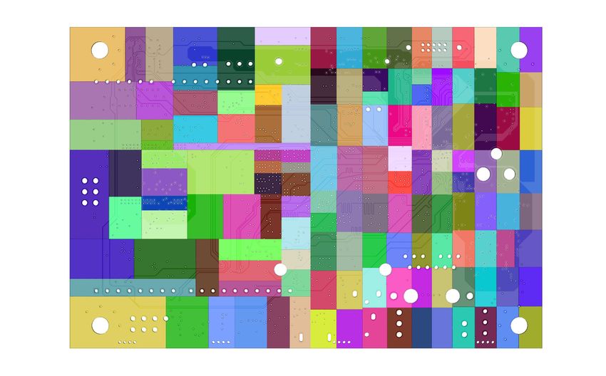
3
Fig. 4: Local surface variables on sub-domain boundaries
Fig. 3: An electronic system with three components
B. Interior Penalty Domain Decomposition Formulation
III. T ECHNICAL A PPROACH To obtain a modular and robust domain decomposition, we
bring out an additional set of variables, the so-called electric
A. Boundary Value Problem trace jm . Together with the naturally induced magnetic trace
Consider an electronic system with an integration of mul- em , we have two sets of local variables on each sub-domain
tiple sub-systems as illustrated in Fig. 3. We are interested boundary ∂Ωm as illustrated in Fig. 4, defined by:
in the EMI and SI analysis among those sub-systems. To
1 (m) 1
do so, we need to solve for the time-harmonic electric field jm = π× ∇×Em (7)
−k0 µrm
within each sub-system, denoted by Em ∈ H0 (curl, Ωm ).
H0 (curl, Ωm ) is the space of curl-conforming functions that em = πτ(m) (Em ) (8)
satisfy essential boundary conditions on the collection of
which represent the (scaled) electric current and the tangential
perfect electric conducting (PEC) surfaces [57].
electric field on ∂Ωm . We remark that through this decom-
In this work, the computational domain Ω is partitioned into
position, the original boundary value problem (BVP) is now
non-overlapping sub-domains, Ω = Ω1 ∪ Ω2 ∪ · · · ΩM . The
replaced by many local and nearly decoupled BVPs within
boundary of sub-domain Ωm is denoted as ∂Ωm . Moreover,
sub-domains. Adjacent sub-domains are coupled through the
we denote Γmn and Γnm for the interfaces between Ωm and
auxiliary surface variables and transmission conditions locally
Ωn with Γmn the surface seen from Ωm and Γnm as the one
at sub-domain interfaces. We can then develop the varia-
from Ωn . Γm denotes the set of all the sub-domain interfaces in
tional weak formulation sub-domain-wise through the interior
the sub-domain, Ωm . Hence, the boundary of mth sub-domain
penalty formulation.
∂Ωm has been decomposed into the domain interface part Γm
fm . 1) Volume Interior Penalty Term: Similar to the standard
and the exterior boundary part ∂Ω
finite element method, the vector wave equation (3) is tested
We introduce two surface trace operators on the boundary with test field vm ∈ H0 (curl, Ωm ). The resulting volume
∂Ωm , the tangential components trace operator πτ (•) and the penalty term, Pm v
(vm , Em ), can be written as:
twisted tangential trace operator π× (•), defined by:
V 1
(m)
π× (um ) := n̂m × um |∂Ωm (1) Pm (vm , Em ) = vm , ∇ × ∇ × Em
µrm
Ωm
πτ(m) (um ) := n̂m × (um × n̂m )|∂Ωm = π× (u) × n̂m (2) − k (vm , εrm Em )Ωm + kη0 vm , Jimp
2
m (9)
Ωm
Consequently, within each sub-domain, the electric field Em After applying the Green’s identity, it becomes:
must satisfy the following vector wave equation and boundary
conditions: V 1
Pm (vm , Em ) = ∇ × vm , ∇ × Em
µrm Ωm
∇×µ−1 2 imp
rm ∇×Em −k0 εrm Em + kη0 Jm = 0 in Ωm (3) − k 2 (vm , εrm Em )Ωm + kη0 vm , Jimp
m Ωm
πτ(m) (Em ) − πτ(n) (En ) = 0 on Γmn (4) D E
(m)
+ kη0 πτ (vm ) , jm
(m) (n) fm
π× µ−1rm ∇×Em + π× µ−1
rn ∇×En = 0 on Γmn (5) X D
∂Ω
E
+ kη0 πτ(m) (vm ) , jm (10)
(m) f m (6)
π× µ−1rm ∇×Em +DtN πτ
(m)
(Em ) = 0 on ∂Ω Γmn
Γmn ∈Γm
Namely, the electric field Em is curl-conforming within each 2) Interface Interior Penalty Term: Equations (4) and (5)
sub-domain Ωm but can be discontinuous across sub-domain enforce the necessary continuities of tangential components
interfaces. Equations (4) and (5) need to be satisfied for all of electric and magnetic fields across the interfaces between
Γmn ∈ Γm , which enforce the necessary field continuity adjacent sub-domains. Moreover, they also determine the
conditions for the tangential components of the electric and convergence behavior of the Schwarz iterative process. In
magnetic fields across the sub-domain interfaces. Equation (6) the literature, a number of transmission conditions (TCs)
f m and the DtN is the
is the exact boundary condition on ∂Ω have been developed to accelerate the convergence [59]–[63].
Dirichlet-to-Neumann operator [58]. The implementation of Among them, we consider a second order (2nd ) TC [53],
DtN will be discussed in detail in the next subsection. which has been proven to provide converging mechanism for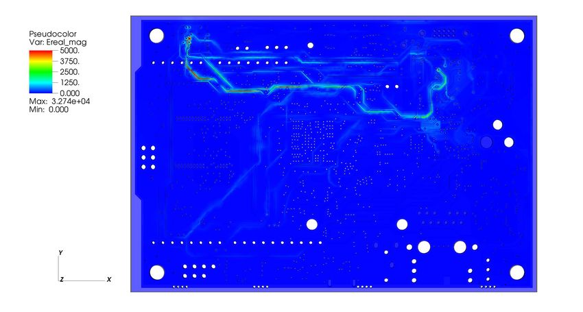
4
both the propagating and evanescent waves on the sub-domain
interfaces. It can be written as:
−η̄m jm + em + κTE TM
m ∇ τ × ∇ τ × em − κ m ∇ τ ∇ τ · j m
= η̄m jn + en + κTE TM
m ∇τ × ∇τ × en + κm ∇τ ∇τ · jn (11)
where η̄m represents the relativepintrinsic impedance in mate-
rial regions defined as η̄m = µrm /εrm . The ∇τ × ∇τ ×
and ∇τ ∇τ · are second order tangential derivatives and τ
denotes the tangential direction. The κTE TM
m and κm are complex Fig. 5: Exterior electric and magnetic traces on the exterior
parameters that can be chosen to obtain rapidly converging DD sub-domain boundary
algorithms. The optimized choices of these parameters and a
detailed theoretical convergence analysis have been discussed
in [64], [65]. ejm (r) ∈ H−1/2 (divτ , ∂Ω f m ) and H−1/2 (divτ , ∂Ωf m ) is the
Next, in order to implement the ∇τ ∇τ · term, an additional function space for divτ -conforming functions on the boundary
scalar variable is further introduced: f m . Similarly, the exterior magnetic trace can be written as
∂Ω LM f m)
ρm = ∇τ · jm on Γmn (12) e
e(r) = m=1 eem (r), where e em (r) ∈ H−1/2 (curlτ , ∂Ω
nd and H −1/2 f
(curlτ , ∂Ωm ) is the function space for curlτ -
Similar to [53], [62], we test the 2 TC (11) with
conforming functions on ∂Ω f m.
wm ∈ H (curlΓ ; Γmn ) and test the definition (12) with
φm ∈ H 1/2 (Γmn ). The resulting interface penalty term on By using those exterior traces, ej and e
e, as input arguments,
Γmn can be written as (after the integration by parts): we can write the following multi-trace combined field integral
equation (MT-CFIE) on ∂Ω f [65] (the combination parameter
I
Pmn (wm , φm ; jm , em , ρm , jn , en , ρn ) is set to be 0.5):
= − η̄m hwm , jm + jn iΓmn + hwm , em − en iΓmn 1 1
e + ej − C× e
e f − Cτ ej; ∂Ω
e × n̂; ∂Ω f = 0 on ∂Ω f (14)
+ κTE
m h∇τ × wm , ∇τ × (em − en )iΓmn 4 4
− κTM
m hwm , ∇τ ρm + ∇τ ρn iΓmn where the combined field integral operator Cαk0 is defined as:
+ κTM TM
m hφm , ρm iΓmn + κm h∇τ φm , jm iΓmn (13) f := π (0) L f ; ∂Ω f (0) f
Cτ f ; ∂Ω τ + π × K̄ f ; ∂Ω (15)
Note that we have scaled the definition equation (12) with κTM m
in order to obtain a balanced interface penalty term. and its rotational counterpart:
3) Boundary Interior Penalty Term: Equation (6) indi- f := π (0) L f ; ∂Ω f f
C× f ; ∂Ω × − πτ(0) K̄ f ; ∂Ω (16)
cates the truncation boundary condition using Dirichlet-to-
Neumann map on ∂Ω f m . Since the exact DtN operator is Note that the superscript of the trace operator indicates the
not easily obtainable for complex geometries, the pseudo- unit norm on ∂Ω f is pointing outward to the exterior space. The
differential operators are commonly used as an approximation electric field boundary potential L and magnetic field boundary
[52], [66], [67]. For instance, when the first (1st ) order potential K are defined as:
absorbing boundary condition (ABC)is employed, we have:
(m)
π× µ−1 ∇×E
+k
(m) f m. f := −k0 ΨA f ; ∂Ω
L f ; ∂Ω f + 1 ∇∇·ΨF f ; ∂Ω f (17)
rm m 0 πτ
η̄ (Em ) = 0 on ∂Ω
k0
However, the use of ABC is not sufficient to represent
f
K f ; ∂Ω := ∇ × ΨA f ; ∂Ω f (18)
accurately the coupling among these sub-domains. In turn,
it cannot accurately characterize the intra-system EM inter-
where ΨA and ΨF are the single-layer vector and scalar
ferences. One of the main contributions of this paper is to
potential, defined by:
apply an interior penalty discontinuous Galerkin (DG) integral Z
equation (IP-DG-IE) formulation as the truncation boundary f (r) :=
ΨA f ; ∂Ω f (r′ )G(r, r′ )dr′ , (19)
condition. The formulation was recently proposed for solving Z f
∂Ω
EM scattering from PEC objects. The formulation leads to f (r) :=
ΨF f ; ∂Ω f (r′ )G(r, r′ )dr′ , (20)
a rapidly-convergent, scalable boundary IE DD method [68], f
∂Ω
and an adaptive, parallel IE solver [69] for very large-scale ′
exp−k0 |r−r |
EM modeling and simulation. and G(r, r′ ) : = 4π|r−r |′ is the free-space Green’s func-
This work extends the IP-DG-IE formulation from PEC tion. Finally, K̄ in (15) and (16) stands for the principle value
cases with only electric traces to general cases involving both of the magnetic field boundary potential, K.
electric and magnetic traces. We first introduce the electric and In the following, we introduce the DG weak formulation
magnetic traces ejm and e em , at individual exterior boundaries, for the solution of Eq. (14). To begin with, we denote by
f m , m = 1, . . . , M , as shown in Fig. 5.
∂Ω Cmn and Cnm the contour boundaries between two adjacent
One direct benefit of the IP-DG-IE formulation is that exterior boundaries ∂Ω f m and ∂Ωf n , by Cmn the contour line
it enables us to construct the boundary element space sub- f f
on ∂Ωm and by ∂Ωnm the contour line on ∂Ω f n . Furthermore,
domain-wise for the unknown traces. The LM total exterior elec- associated with each sub-domain contour, Cmn , we define a
tric trace can be written as ej(r) = e
m=1 jm (r), where unit normal t̂mn , which points from sub-domain ∂Ω f m toward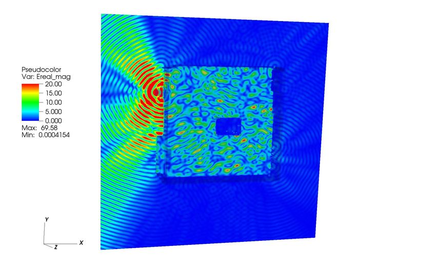
5
sub-domain ∂Ω f n . Since the in-plane components of exterior be expressed as:
traces may be discontinuous across contour boundaries, we
TC e
first introduce the following jump operator: Pm e m , wm ; ejm , e
λm , w em , j m , em
D E D E
= η̄m λ em , ejm + jm − λ em , e
em − e m
f fm
JuKmn := t̂mn · um − t̂mn · un on Cmn . (21) D E∂Ωm ∂Ω
− η̄m w e m , ejm + jm + hw e m, eem − em i∂Ω
fm
f
D E∂Ωm
Ther normal
z jump of the exterior trace ej can be expressed − η̄m wm , jm + ejm + hwm , em − e em i∂Ω
fm (23)
fm
∂Ω
as j e . The tangential jump of the exterior trace e
e can
mn 4) Variational Weak Formulation: With the above dis-
be written as Je e × n̂Kmn . In addition, the vector
R and scalar cussions, the complete variational weak formulation can be
inner products areRdefined by hx, yi∂Ω f m : = ∂Ωf m x • y ds formally stated as:
and hx, yi∂Ω f m := ∂Ωf m xy ds, respectively. Find E = ⊕M M
m=1 Em , Em ∈ H0 (curl, Ωm ); j = ⊕m=1 jm ,
To simplify the notations for the DG weak formulation, we M
jm ∈ H (curlΓ ; Γm ); ρ = ⊕m=1 ρm , ρm ∈ H 1/2
(Γm ); ej =
M e e −1/2 f LM
first define the following bilinear form: ⊕m=1 jm , jm ∈ H (divτ , ∂Ωm ); and, e
e = m=1 e em ,
f m ) such that
em ∈ H−1/2 (curlτ , ∂Ω
e
* +
k0 X
M XM M
X
a (v, u) := vm , f
ΨA un ; ∂Ωn V
Pm e w;
(vm , Em ) + P BI λ, e ej, e
e
2 m=1 n=1 f
∂Ω m=1
* +m
1 X
M XM M
X X
+ ∇τ · v m , fn
ΨF ∇τ · un ; ∂Ω + I
Pmn (wm , φm ; jm , em , ρm , jn , en , ρn )
2ık0 m=1 n=1 f
∂Ω m=1 Γmn ∈Γm
* + m
1 X XM M
X
+ JuKmn , fn
ΨF ∇τ · vn ; ∂Ω + TC e
Pm e m , wm ; ejm , e
λm , w e m , j m , em = 0 (24)
4ık0 n=1
Cmn ∈C C m=1
* + mn
X XM ∀v = ⊕M M
1 fn m=1 vm , vm ∈ H0 (curl, Ωm ); ∀w = ⊕m=1 wm ,
− JvKmn , ΨF ∇τ · un ; ∂Ω M
wm ∈ H (curlΓ ; Γm ); ∀ψ = ⊕m=1 ψm , ψm ∈ H 1/2
(Γm ),
4ık0 n=1
Cmn ∈C Cmn e = ⊕M λ em , λem ∈ H−1/2 (divτ , ∂Ω f m ); and, w
λ m=1 e =
X M LM
β 1 X m=1 e
w m , e
w m ∈ H −1/2
(curl τ , f m) .
∂Ω
+ hJvKmn , JuKmn iCmn + hvm , um i∂Ω
fm
2k0 4 m=1
Cmn ∈C
* + C. Multi-Scale and Parallel Computation
1 X
M XM
+ n̂ × vm , fn
K̄ un ; ∂Ω The mathematical ingredients of this work enable an adap-
2 m=1 n=1 f ∂Ωm tive, parallel and scalable computational framework well-
suited for advanced distributed computing systems. Both the
where the stabilization parameter [68] is chosen to be β = EM field quantities of interest and full-wave analysis are for-
logh̄ /10, where h̄ is the average element size over the entire mulated on the geometry representation of individual electrical
discretization. We notice that even though it may not be the components. It allows generating analysis-suitable models per-
optimal choice, it leads to a robust and easy implementation component, analyzing individual components independently,
for the geometrically non-conformal DD partitioning. Another and automating assembly of multiple components to obtain
choice could be choosing h̄ locally for each pair of sub- the virtual prototyping of entire product. Such a component-
domains. The comparison of two choices will be reported in oriented analysis framework provides flexibility and conve-
the future work. nience for the fast turn-around electrical design automation,
since it is possible to only update the portion of the geometry
Following the Galerkin procedure, the MT-CFIE (14) is
that has changed during the design process.
tested twice L with sub-domain-wise curlτ -conforming func-
M 1) Discrete Formulation: In the context of discrete meth-
tions we = we (r) and divτ -conforming functions
e LM e m=1 m f The boundary ods, individual sub-domains can be discretized independently
λ = m=1 λm (r) on the exterior boundary ∂Ω. from the others. Based on the variational weak formulation
interior penalty term with the MT-CFIE can be expressed as: (24), each sub-domain consists of a volume finite element
part in Ωm , and a boundary integral (BI) part on ∂Ω f m.
e w;
P BI λ, e ej, e
e = a λ,e ej + a λe × n̂, e
e × n̂ Subsequently, volume tetrahedral meshes are employed for the
local FE part and surface triangular meshes are used for the
e ej + a (w
+ a w, e × n̂, e
e × n̂) (22) local BI part. Fine surface discretizations are generated locally
to accurately represent complex geometries. Individual sub-
domains contain their own collection of tetrahedra, triangles,
Finally, these exterior traces will couple to interior FE traces edges and vertices. This attractive feature enables a trivially
through Robin-type TCs on each sub-domain boundary ∂Ω f m. parallel mesh generation and and allows engineers to rapidly
The resulting boundary interior penalty term with the TCs can generate high-fidelity models of complex electronics.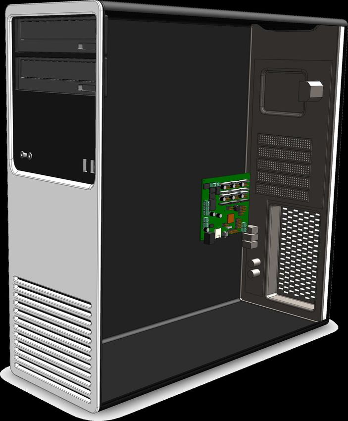
6
Specifically, for each of the sub-domains, the solution vector
the rest of the unknowns. Namely, the CFEmn only involves the
may contain six components, e.g. xm = xFE m | xm
BI
= sub-domain surface FE tangential traces.
b T
Em esm jm s
ρsm | ebm jm , including: the coefficients of vec- We introduce a simple restriction operator, Rm , for FE
tor field Em inside Ωm ; esm for the coefficient vector of Em on coefficient vector xFE
m . Specifically, we have:
s
the sub-domain boundary ∂Ωm ; jm for the coefficient vector
of jm on the sub-domain surface ∂Ωm ; ρsm for the coefficient 0 I 0 0
vector of ρm on the sub-domain interface Γm ; ebm and jm b Rm = 0 0 I 0 (27)
for the coefficient vectors of e em and ejm on the sub-domain 0 0 0 I
exterior boundary. and,
The matrix equation resulted from the finite dimensional
esm
discretization can be written as the following compact form: Rm xFE FE
= jms
m = x̄m (28)
(for simplicity, we use the three sub-domains illustrated in Fig. ρms
3 as an example)
Furthermore, it is easy to show that
A1 C12 C13 x1 b1
C21 A2 C23 x2 = b2 (25)
CFE T FE T T FE
mn = Rm Rm Cmn Rn Rn = Rm C̄mn Rn (29)
C31 C32 A3 x3 b3
where Am denotes the matrix for the mth sub-domain, and (2) Projection from boundary BI unknowns to skeleton
Cmn is the coupling matrix between sub-domains. Moreover, unknowns: Next, we investigate the use of multi-level skele-
we have: tonization to construct effective basis functions for the fine-
FE FE scale structures. The skeletonization scheme can be viewed
Am AFB m Cmn 0
Am = Cmn = (26) as a compressed (“data-sparse”) representation of structured
ABF
m ABI
m 0 CBI
mn
rank-deficient matrices. It has been applied to the compression
We remark that coupling matrices Cmn can be divided into of low rank matrices via the interpolative decomposition [90],
two categories: (i) sparse sub-matrices CFE mn referring to FE [91], and the development of fast direct solvers for elliptic
interface coupling between adjacent sub-domains; (ii) dense operators [92]–[94]. Here we extend the previous work [89],
sub-matrices CBI mn referring to BI radiation coupling, which [95], [96] and use the skeletonization scheme to build effective
requires that the surface currents in each independent sub- basis functions for overly dense boundary discretizations.
domain be radiated to all other sub-domains. The separable First, Huygens’ surfaces are introduced for individual sub-
matrix structure enables the possibility of applying suitable domains to facilitate the selection of the skeleton basis func-
matrix compressing approaches for the efficient multi-scale tions [89]. Thus, the skeletonization can be achieved locally
and parallel computation, as discussed in the following section. per sub-domain and in parallel. The mapping of original BI
2) Multi-Scale Computation: One of the challenges in the unknowns to skeleton unknowns can be written as:
full-wave analysis of IC and electronics is the multi-scale
modeling of different components with different scales. Many x̄BI BI
m = Pm x m (30)
methods have been proposed to address the computational
complexity of multi-scale EM and circuit simulations, includ- where Pm is the projection matrix. The BI coupling matrices
ing hierarchical bases [70]–[72], multi-grid methods [73]–[76], between sub-domains can then be decomposed as:
equivalence principle algorithms [51], [77], macromodeling
[78]–[82] and reduced order models [83]–[88]. CBI T BI
mn ≈ Pm Smn Pn (31)
In this work, we develop a rigorous, error controllable, and
The SBI
mn is the dense coupling matrix between the skeletons
parallelizable scheme to reduce the computational complex-
of two corresponding sub-domains. Moreover, it is a subset of
ity in the multi-scale computation. For IC and electronics
CBI
mn and its matrix entires can be computed exactly the same
of interest, very fine discretizations are usually required to
way as CBImn .
accurately represent complex geometries. We first employ the
multi-level skeletonization [89] to build effective “coarse-grid” By combining (29) and (31), the coupling matrix Cmn can
basis functions. These “coarse-grid” bases are selected from be written as:
T FE
the original basis functions on overly dense discretizations, Rm 0 C̄mn 0 Rn 0
without the need to construct nested meshes as in multi- Cmn =
0 PTm 0 SBI
mn 0 Pn
grid methods. Hence, they are termed as the skeleton basis. T
= Vm C̄mn Vn (32)
Subsequently, the interactions between sub-systems will be
computed using selected skeletons, and the DD iteration will (3) Preconditioned DD system: After applying (32) to the
be performed on the skeleton-based compressed system. We original matrix equation (25), the result can be expressed as:
will progressively elaborate the DD matrix solution procedure
as the following three steps: A1 V1T C̄12 V2 V1T C̄13 V3 x1 b1
(1) Restriction from volume FE to surface unknowns : One V2T C̄21 V1 A2 V2T C̄23 V3 x2 = b2
appearing feature of the matrix equation in (25) is that the V3T C̄31 V1 V3T C̄32 V2 A3 x3 b3
interior FE unknown coefficients are almost decoupled from (33)
7
Subsequently, we employ a one-level non-overlapping additive its own appropriate sub-domain solver based on local EM
Schwarz preconditioner [53], and use only the inverse of sub- wave characteristics and geometrical features. Furthermore,
domain matrices, namely, we have developed a queue-based task balancing strategy. The
time spent for individual tasks in the previous DD iteration is
I A−1 T
1 V1 C̄12 V2 A−1 T
1 V1 C̄13 V3 x1
A−1 T −1 T measured, and the tasks are sorted and recorded into a task
2 V 2 C̄ V
21 1 I A 2 V 2 C̄ V
23 3 x 2
−1 T −1 T queue. Each MPI process will be assigned with a group of
A3 V3 C̄31 V1 A3 V3 C̄32 V2 I x 3
−1 T tasks based on the timing data, leading to a dynamic load
−1 −1 balancing environment.
= A1 b 1 A2 b 2 A3 b 3 (34)
The second part in the parallel computing is the coupling
Finally, we apply the projection matrix Vm on both sides of among multiple sub-domains, C̄mn . It consists of two type of
equation (34), which results in sub-matrices: (i) interface coupling referring to sparse matrices
I Z1 C̄12 Z1 C̄13 x̄1 b̄1 C̄FE
mn , which only requires communications between adjacent
Z2 C̄21 I Z2 C̄23 x̄2 = b̄2 (35) sub-domains through touching interfaces. This is particularly
Z3 C̄31 Z3 C̄32 I x̄3 b̄3 suitable for distributed memory supercomputers; (ii) radiation
coupling regarding to dense matrices, Smn , which requires
where x̄m contains only the FE surface unknowns and BI that the surface currents in each independent sub-domain be
skeleton unknowns, and radiated to all other sub-domains.
Zm = Vm A−1 T −1 As alluded earlier, one particularly interesting aspect of
m Vm , b̄m = Vm Am bm (36)
the skeleton matrix Smn is that its matrix entries belong to
The preconditioned matrix equation (35) will be solved by a a subset of CBI mn . As a result, the multilevel fast multipole
Krylov subspace iterative method. Once the reduced unknown method (FMM) [97], [98] can be directly applied to speed
vector x̄m is computed, the solution for each sub-domain can up the matrix-vector multiplication. Furthermore, to achieve
be recovered through backward substitutions. high parallelization efficiency, we have utilized a primal-
In summary, instead of directly applying Schwarz DD dual octree partitioning algorithm aiming for separable sub-
scheme to the original full-scale system with a total number of domain couplings. Namely, instead of partitioning the entire
N degrees of freedom (DOFs), we construct a coarse-grained computational domain into a single octree as in the traditional
compressed system to reduce the DD matrix dimension from FMM, we first create independent octrees for all sub-domains.
O(N ) to O(M ), where M is the number of surface FE and Those octrees are allowed to be overlapping or intersecting.
skeletoned BI unknowns. A dramatic reduction in computa- Both the skeletonization and aggregration/disaggregration can
tional complexity is expected since M will be a much smaller be computed locally per sub-domain and in parallel.
number than N regarding to 3D IC and electronics applications In summary, the appealing parallel simulation capabilities
of interest. including: (i) high data locality property, which consists of
3) Parallel Computing: To fully exploit the recent suc- embarrassingly parallel model preparation, concurrent mesh
cess of multi-core processors and massively parallel dis- generation and trivially parallel sub-domain solutions. Essen-
tributed memory supercomputers, we have considered a hybrid tially, all large-scale data structures will be distributed among
MPI/OpenMP implementation of proposed algorithms. The processors; (ii) parallel skeletonization scheme, separable cou-
computation in solving the preconditioned DD matrix equation pling procedure, and offline construction of the computing
(35) can be divided into two parts: (i) the application of the block database; (iii) the optimized Schwarz transmission con-
additive Schwarz preconditioner involving local sub-domain ditions at FE interfaces and the DG coupling at BI boundaries
solutions, Zm ; and (ii) the coupling among sub-domains result in scalable convergence in the iterative solution of the
corresponding to off-diagonal matrices, C̄mn . preconditioned DD systems.
One advantage of the proposed preconditioner is the ability
to solve all the sub-domain problems simultaneously in each
IV. N UMERICAL E XPERIMENTS
DD iteration. For common types of components in IC and
package layout, we may explicitly construct the sub-domain In this section, we present numerical experiments to access
matrix Zm . These component-wise sub-domain matrices are the performance and to illustrate the capability of the proposed
stored as the computing block database, and can be used for all work. The discussion is organized into two parts. The first
future online assembly and simulation. For electrically large part is to study the numerical performance of the method,
sub-domains, the matrix Zm can be realized implicitly through including the convergence analysis of DD method, the multi-
another preconditioned Krylov method (inner-loop iteration). scale computing using skeleton bases, and the validation of
In the parallel implementation, we have employed a task- the solution accuracy. The second part is the application of
based parallelism for sub-domain solutions. Namely, those the work to electronics of practical interest, including the full-
sub-domain solutions are considered as independent tasks wave analysis of a product-level PCB and the intra-system
in an MPI programming model. Individual MPI processes EMI analysis of a computer box with multiple electronic
will execute different tasks simultaneously. The parallelization components.
within each task is attained using OpenMP, which exploits We solve the preconditioned DD matrix equation (35) via a
the fast memory access in the shared-memory multi-core parallel Krylov subspace iterative method, Generalized Con-
processors. Therefore, each sub-domain is allowed to choose jugate Residual (GCR) [99] with the truncation size to be 10
8

                                                 120 mm
     y

                                                                              15 mm
 x                                                    PEC trace

                       45 mm
                                                                                      15 mm

                                                    30 mm
            60 mm

                                                                  1.2 mm

                    15 mm      r = 1.38 mm                            45 mm

                                                                                                1.5 mm
                                                PEC trace
         3 mm

 z
     y              Port 1      rin = 0.6 mm                            Port 2
                                                             1.5 mm                    1.5 mm
                               rout = 1.38 mm   PEC ground

          Fig. 6: Geometry of a microstrip transmission line

[100]. Each sub-domain Krylov subspace vector is stored only
in the local memory associated with individual MPI processes.                                             (a) Geometry-based partitioning                  (b) Graph partitioning
The relative residual in the Krylov iterative solver is designated
                                                                                                         Fig. 7: Illustration of sub-domain partitioning strategies
as ǫ = 10−3 unless specified otherwise. Experiments were
conducted on Copper, a Cray XE6m DoD HPCMP Open
Research System. Copper has 460 compute nodes that share
memory only on the node; memory is not shared across the
nodes. Each compute node has two sixteen-core processors (32
cores per node) that operate under a Cray Linux Environment
(CLE) sharing 64 GBytes of DDR3 memory.                                                                                 0

                                                                                                                       -5
A. Performance Study
   1) Convergence Study: The first numerical example is a                                                             -10
                                                                                                           S11 (dB)

microstrip transmission line with two coaxial cable ports. The
PEC trace is embedded in the middle of a FR4 dielectric                                                               -15

substrate. The thickness of the substrate is 3 mm and the
relative permittivity of the dielectric material is 4.5. The                                                          -20
                                                                                                                                                                Regular Partition
geometry details are given in Fig. 6. To highlight the flexibility                                                                                              Irregular Partition

of the method, we consider two domain partitioning strategies.                                                        -25
                                                                                                                            5       6            7         8           9              10
The first case is the geometry-based partitioning, in which                                                                                    Frequency(GHz)
the sub-domains are formed by a direct decomposition of the                                                                                 (a) S11 parameter
original problem geometry by transverse cutting planes. The
second case is the algorithmic graph partitioning using METIS                                                          0
[101]. We first generate quasi-uniform tetrahedral meshes of
the entire geometry, and then partition the mesh into equally
sized sub-domains with nonplanar interfaces . The resulting                                                           -5
sub-domain partitionings are depicted in Fig. 7. In both cases,
                                                                                                         S12(dB)

each sub-domain consists of a volume FE part, Ωm , and a
                  f m.                                                                                             -10
surface BI part ∂Ω
   The simulation is performed over a high frequency band (5
GHz - 10 GHz). The calculated S11 and S12 parameters using                                                         -15
the two domain partitionings are depicted in Fig. 8. We see that                                                                Regular Partition
the regular partitioning (resulting from the geometry-based                                                                     Irregular Partition
strategy) and the irregular partitioning (resulting from graph                                                     -20
                                                                                                                            5       6            7         8           9              10
partitioning) give identical solutions. The numbers of iterations                                                                            Frequency(GHz)
required for the two cases are given in Fig. 9. The convergence                                                                             (b) S12 parameter
curves maintain a relative constant rate with respect to the
operating frequency. Lastly, Figure 10 presents the surface                                                   Fig. 8: The comparison of calculated S parameters
magnetic current distributions at 5 GHz, where we notice that
the two cases agree very well.
9

                            100
                                                               Regular Partition
                                                               Irregular Partition
                             80
     Number of Iterations

                             60

                             40

                             20

                              0
                                  5   6    7          8               9              10
                                          Frequency(GHz)

                                                                                             Fig. 11: The geometry of a mock-up multi-scale object
 Fig. 9: Number of iterations for the microstrip simulation
                                                                                               TABLE I: Statistics of the skeleton basis functions

                                                                                                          Sub-domain         1     2       3
                                                                                                        Original DOFs       553   1812   11750
                                                                                                     Skeleton DOFs (5 G)    274   787     581
                                                                                                     Skeleton DOFs (10 G)   274   792     543

                                                                                          number of the skeleton basis functions is given in Table I,
                                                                                          where a reduction of 20 times is achieved in comparison
                                                                                          with the original basis functions in both operating frequencies.
                                                                                          Moreover, the iterative solver convergences for the original
                                                                                          DD system without compression and the skeletonized DD
                                                                                          system are plotted in Fig. 13. The calculated far-field for
                                                                                          two frequencies are given in Fig. 14. We notice that the
                                                                                          the skeletonized DD system requires less iteration counts
                                                                                          to converge, and produces nearly identical far-field patterns
   (a) Geometry-based partitioning                         (b) Graph partitioning         comparing to the original DD system.
                                                                                             3) Validation Example: We conclude this subsecton with
Fig. 10: Surface magnetic currents on the top surface of the
                                                                                          a validation example by simulating two monopole antennas
microscrip transmission line at 5 GHz.
                                                                                          mounted inside a closed surface PEC cavity. The compu-
                                                                                          tational domain is decomposed into three components: 1)
                                                                                          interior cavity case; 2) long monopole; and 3) short monopole,
   2) Multi-Scale Analysis: To demonstrate the benefit of                                 as shown in Fig. 15. The geometry of each monopole is also
skeleton basis functions in the multi-scale analysis, we create a                         illustrated. After decomposition, the IP-DG-IE formulation
mock-up object, whose geometry consists of three components                               [102] is used to discretize the cavity sub-domain Ω1 , and the
with different scales, as illustrated in Fig. 11. For the sake of                         volume FE method is employed to discretize the antenna sub-
simplicity, we assume the object is PEC and the excitation                                domains Ω2 and Ω3 . In the simulation, we excite the short
is an external plane wave illumination from −ẑ direction.                                monopole and use the long monopole as the receiving antenna.
The solution vector is the surface electric trace ej on the                               The computed S11 and S12 with respect to different operating
exterior boundary. The simulation is performed at two different                           frequencies are shown in Fig. 16. The measurement results
frequencies: 5 GHz and 10 GHz.                                                            conducted in Applied EM Group at University of New Mexico
   The sub-domains are formed by a geometry-based parti-                                  (UNM) are also given in Fig. 16. Very good agreement is
tioning, resulting in three sub-domains for three components.                             observed between the results obtained by computation and
All three sub-domains are discretized independently. The                                  measurement.
discretization size is based on the characteristic size of the
component. As depicted in Fig. 12(a), the surface discretiza-
tions are non-conformal along the contour boundaries between                              B. Application Study
adjacent sub-domains. Next, Figure 12 (b) and (c) present                                    1) Signal Integrity of PCB Interconnects: To examine the
the skeletoned discretizations at two operating frequencies.                              performance of the work on practical electronics of interest, a
We see that the original fine surface discretizations are suc-                            product-level PCB, Intel Galileo Development Board, is con-
cessfully coarsened and the selected triangular meshes are                                sidered in this study. The detailed Galileo datasheet is provided
mostly around the edges and corners in the geometry. The                                  in [103]. The geometry and the high intensity interconnects
10

                                                                                  10 -1
                                                                                                                                Original DD System
                                                                                                                                Skeletoned DD System

                                                                                  10 -2

                                                                                  10 -3

                                                                       Residual
                                                                                  10 -4

                                                                                  10 -5
                     (a) Original surface mesh

                                                                                  10 -6
                                                                                          0       5        10         15         20         25         30
                                                                                                                 Iterations
                                                                                                                (a) 10 GHz

                                                                                  10 0
                                                                                                                                Original DD System
                                                                                                                                Skeletoned DD System
                                                                                  10 -1

                                                                                  10 -2

                                                                       Residual
                                                                                  10 -3

                  (b) Skeletoned mesh at 10 GHz
                                                                                  10 -4

                                                                                  10 -5

                                                                                  10 -6
                                                                                          0   5       10         15        20         25     30        35
                                                                                                                 Iterations
                                                                                                                (b) 5 GHz

                                                                   Fig. 13: Iterative solver convergences for the multi-scale object

                                                                   solver requires 29 iterations to converge, and the computation
                   (c) Skeletoned mesh at 5 GHz                    takes 2 minute per DD iteration. The electric and magnetic
                                                                   fields for the large multi-scale simulation are plotted in Fig.
Fig. 12: Domain partitioning and surface discretizations for       18.
the multi-scale object                                                2) Intra-System EMI of Electronics: The second numerical
                                                                   example is the intra-system EMI analysis of a complex elec-
                                                                   tronic system as shown in Fig. 19(a). There are two monopole
are depicted in Fig. 17 (a) and (b). The total thickness of        antennas located at the back case of the computer. These two
the PCB interconnect is slightly more than 2.36 mm. After          antennas are connected to the Intel Galileo PCB inside the
a geometry-based partitioning, the 3D geometry is divided          computer box through two coaxial cables. We are interested
into 141 sub-regions by transverse planes, as illustrated in       in both the EM conductive and radiative coupling to the PCB
Fig. 17 (c). All sub-regions are discretized independently and     interconnect when the monopole antenna is turned on. The
concurrently. Attributed to the benefit of non-conformal FE        operating frequency is 10 GHz. As illustrated in Fig. 19,
DD and IE DG formulations, both the volume discretizations         individual sub-systems exhibit vast differences in the aspect
on the FE interfaces and the surface discretizations on the BI     ratios (ratio of wavelength to feature size).
boundaries can be non-matching. The simulation requires a             We employ a hierarchical domain partitioning strategy. The
total number of 43,508,700 DOFs for the FE unknowns and            electronic system is firstly divided into the computer box,
39,204 DOFs for the BI unknowns. In the parallel computing,        antennas, coaxial cables and PCB sub-systems. Each sub-
we assign each FE sub-domain with one MPI process in which         system is further decomposed into sub-domains based on
16 OpenMP threads are used. To achieve a load balanced             the number of processors available and the local memory
computation, we group the BI unknowns into a single sub-           each processor can access. For example, the computer case
domain and assign it to one MPI process. Thus, a total number      is decomposed into 8 sub-domains following the graphic
of 142 sub-domains and 2272 computing cores are used in            partitioning strategy. The PCB interconnect is decomposed
the computation. The simulation is conducted at 5 GHz with         into 80 sub-domains based on a geometry-based partitioning.
the port 1 as the excitation port. The parallel Krylov iterative   Due to the complexities of the entire system, the simulation
11
76.20 76.20
10 66.04 66.04
Original DD System
Skeletoned DD System
13.688
0 25.40 25.40
22.634
-10
Ω2
Far field(dBsm)
2.540
Ω2 Ω1
76.20
66.04
-20
Ω1
-30 Ω3 Ω3
15.212
13.688
3.048
-40
Unit: cm
-50
-180 -120 -60 0 60 120 180 (a) Enclosure
Theta(degree)
(a) 10 GHz 5.588
7.112
L0.7L0.7 Ω2 0.635 0.635 L0.635φ0.635 L0.4φ704
Ω3
L0.4φ0.4
φ1.270
φ1.270
0 L0.783L0.783
L1.0φ0.833 L0.4φ0.704
Original DD System
L0.635φ0.635 L0.8φ0.833
-5 Skeletoned DD System L0.6φ0.704
L0.6φ0.833 L0.6φ0.833 L0.6φ0.833 L0.3φ0.704
L0.3φ0.704 L0.6φ0.653
8.128
-10 L0.6φ0.704 L0.6φ0.704
L0.1φ0.577
10.160
L0.5φ0.704 L0.8φ0.833 L0.127φ0.193 PEC surface
Far field(dBsm)
-15 L0.4φ0.610 L0.8φ0.833
L0.127φ0.191 L1.891φ0.193
PEC surface L1.2φ0.704
Teflon
-20 L1.797φ0.191 Teflon
L0.8φ0.833 PEC Pole
L1.582φ0.0508
-25
L1.824φ0.0508 PEC Pole Unit: cm
-30 L:length
φ:diameter
-35
(b) Antennas
-40
-180 -120 -60 0 60 120 180 Fig. 15: Configuration of the validation example and geometry
Theta(degree)
of the antennas
(b) 5 GHz
Fig. 14: Calculated far-field patterns for the multi-scale object
requires 66 million DOFs with a total number of 92 sub-
domains. Each sub-domain is assigned to one MPI process
with 32 computing cores. A total number of 2944 computing
cores are used in the computation. After the skeletonization,
we obtain a coarse-grained compressed DD system with a total
number of 4.9 millions DOFs for the FE interface and BI
surface unknowns. The simulation takes 4 minutes for one
DD iteration and 18 iterations are required to converge. The
EM field distributions with respect to the monopole antenna
radiation at 10 GHz are given in Fig. 20. The calculated
S-parameters for the six ports on the PCB interconnect are
4.12e-04, 9.12e-04, 2.14e-04, 1.03e-04, 1.65e-04 and 1.46e- Fig. 16: Comparison of S-parameters obtained by computation
04, respectively. The location of the six ports are depicted and measurement.
in Fig. 17 (b). The magnitude of S-parameters for port 1
and port 2 are bigger than others due the presence of both
conductive and radiative coupling. The results show that the The resulting EM interference among different components
method is promising to simultaneously simulate heterogeneous within a system may significantly affect the in-situ perfor-
sub-systems exhibiting vast differences in the aspect ratios, mance of individual components. This paper elaborates on
and provides concurrent resolution of multiple scales in the the flexibility, scalability, and efficiency of the computational
computational domain. methods for the intra-system analysis of 3D product-level IC
electronics. The advancements will enable IC and electronics
designers to quickly create and analyze virtual prototypes of
V. C ONCLUSION
products. By simultaneously consider mutual interactions of
Next-generation electronic systems are evolving rapidly to circuits, 3D interconnects, packages and PCBs, it will serve
achieve greater functionality and lower cost with smaller size. as a powerful verification tool in the design stage. As a result,12
(a) Electric field
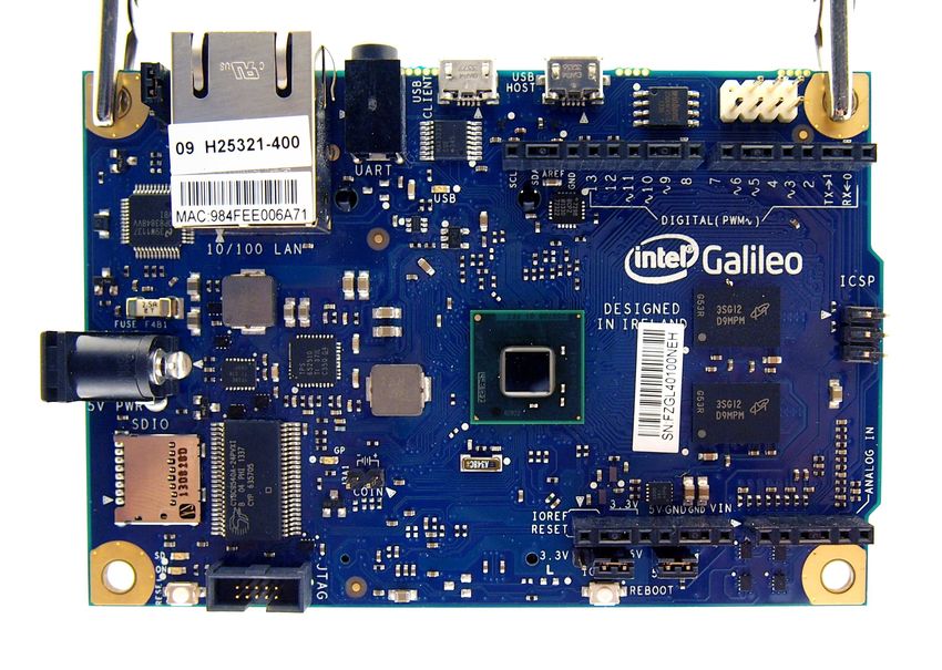
(a) Top view of the Intel Galileo board [103]
port 2
port 1
port 3 port 5 port 6
port 4
(b) Magnetic filed
Fig. 18: The calculated EM field distributions for the Intel
Galileo board
it is expected to dramatically improve our ability to develop
and predict the behavior of modern and future complex IC
systems, while maintaining a high level of confidence on the
in-situ performance.
(b) The traces and interconnects
We remark that the proposed methods do not fundamentally
address the low frequency breakdown problems, although
the direct solver and skeletonization technique alleviate the
computational burden of strongly non-uniform discretizations
and multi-scale computing. One direction for future research
is integrating the treatments of low frequency breakdown for
both FE and BI formulations. Another direction of future
research is investigating an efficient hybridization of full wave
frequency domain and time domain Maxwell solvers, since
the simulations of non-linear components in IC and electronic
systems are more easily tackled in time-domain.
ACKNOWLEDGMENT
The authors would like to thank anonymous reviewers for
(c) Geometry-based partitioning their comments and suggestions. The authors would also like
Fig. 17: Geometry and domain partitioning for the Intel to thank Ms. Ghadeh Hadi, Dr. Sameer Hemmady and Dr. Edl
Galileo board Schamiloglu in Applied Electromagnetics Group at University
of New Mexico for the experiment and measurement results
for the validation example.
R EFERENCES
[1] L. Benini and G. De Micheli, “Networks on chips: a new SoC
paradigm,” Computer, vol. 35, pp. 70–78, Jan 2002.13
Excitation antenna
(a) Problem statement
(a) Electric field
(b) Magnetic field
(b) Computational partitioning
Fig. 19: A complex electronic system and the computational Fig. 20: The calculated EM field distributions for the computer
partitioning system
sis for mixed-signal system implementation: system-on-chip or system-
[2] K. Banerjee, S. Souri, P. Kapur, and K. Saraswat, “3-D ICs: a novel chip on-package?,” IEEE Trans. Electron. Packag. Manufact., vol. 25,
design for improving deep-submicrometer interconnect performance pp. 262–272, Oct 2002.
and systems-on-chip integration,” Proc. IEEE, vol. 89, pp. 602–633, [10] K. S. Yang, S. Pinel, I. K. Kim, and J. Laskar, “Low-loss integrated-
May 2001. waveguide passive circuits using liquid-crystal polymer system-on-
[3] D. Bertozzi, A. Jalabert, S. Murali, R. Tamhankar, S. Stergiou, package (SOP) technology for millimeter-wave applications,” IEEE
L. Benini, and G. De Micheli, “NoC synthesis flow for customized Trans. Microwave Theory Tech., vol. 54, pp. 4572–4579, Dec 2006.
domain specific multiprocessor systems-on-chip,” IEEE Transactions [11] A. Shamim, M. Arsalan, L. Roy, M. Shams, and G. Tarr, “Wireless
on Parallel and Distributed Systems, vol. 16, pp. 113–129, Feb 2005. dosimeter: System-on-chip versus system-in-package for biomedical
[4] L.-R. Zheng, X. Duo, M. Shen, W. Michielsen, and H. Tenhunen, “Cost and space applications,” IEEE Trans. Circuits Syst. II, Exp. Briefs,
and performance tradeoff analysis in radio and mixed-signal system- vol. 55, pp. 643–647, July 2008.
on-package design,” IEEE Trans. Adv. Packag., vol. 27, pp. 364–375, [12] J.-L. Kuo, Y.-F. Lu, T.-Y. Huang, Y.-L. Chang, Y.-K. Hsieh, P.-J. Peng,
May 2004. I.-C. Chang, T.-C. Tsai, K.-Y. Kao, W.-Y. Hsiung, J. Wang, Y. Hsu,
[5] S. K. Lim, “Physical design for 3D system on package,” IEEE Des. K.-Y. Lin, H.-C. Lu, Y.-C. Lin, L.-H. Lu, T.-W. Huang, R.-B. Wu,
Test. Comput., vol. 22, pp. 532–539, Nov 2005. and H. Wang, “60-GHz four-element phased-array transmit/receive
[6] V. Madisetti, “Electronic system, platform, and package codesign,” system-in-package using phase compensation techniques in 65-nm flip-
IEEE Des. Test. Comput., vol. 23, pp. 220–233, May 2006. chip CMOS process,” IEEE Trans. Microwave Theory Tech., vol. 60,
[7] I. Ju, Y. Kim, S. Lee, S. Song, J. Lee, Changyul-Cheon, K.-S. Seo, and pp. 743–756, March 2012.
Y. Kwon, “V-band beam-steering ask transmitter and receiver using [13] D. Appello, P. Bernardi, M. Grosso, and M. Reorda, “System-in-
bcb-based system-on-package technology on silicon mother board,” package testing: problems and solutions,” IEEE Design Test of Com-
IEEE Microwave Wireless Compon. Lett., vol. 21, pp. 619–621, Nov puters, vol. 23, pp. 203–211, May 2006.
2011. [14] S. Y. Yu, Y.-M. Kwon, J. Kim, T. Jeong, S. Choi, and K.-W. Paik,
[8] S. Song, Y. Kim, J. Maeng, H. Lee, Y. Kwon, and K.-S. Seo, “Studies on the thermal cycling reliability of BGA system-in-package
“A millimeter-wave system-on-package technology using a thin-film (SiP) with an embedded die,” IEEE Trans. Comp., Packag., Manufact.
substrate with a flip-chip interconnection,” IEEE Trans. Adv. Packag., Technol., vol. 2, pp. 625–633, April 2012.
vol. 32, pp. 101–108, Feb 2009. [15] V. Kripesh, S. W. Yoon, V. Ganesh, N. Khan, M. Rotaru, W. Fang, and
[9] M. Shen, L.-R. Zheng, and H. Tenhunen, “Cost and performance analy- M. Iyer, “Three-dimensional system-in-package using stacked silicon14
platform technology,” IEEE Trans. Adv. Packag., vol. 28, pp. 377–386, [36] F. Bilotti, S. Lauro, A. Toscano, and L. Vegni, “Efficient modeling
Aug 2005. of the crosstalk between two coupled microstrip lines over noncon-
[16] P. Pulici, G. Vanalli, M. Dellutri, D. Guarnaccia, F. Lo Iacono, ventional materials using an hybrid technique,” IEEE Trans. Magn.,
G. Campardo, and G. Ripamonti, “Signal integrity flow for system-in- vol. 44, pp. 1482–1485, June 2008.
package and package-on-package devices,” Proc. IEEE, vol. 97, pp. 84– [37] C. Buccella, M. Feliziani, and G. Manzi, “Three-dimensional FEM
95, Jan 2009. approach to model twisted wire pair cables,” in 12th Biennial IEEE
[17] Y.-P. Zhang and D. Liu, “Antenna-on-chip and antenna-in-package Conference on Electromagnetic Field Computation, 2006, pp. 384–384,
solutions to highly integrated millimeter-wave devices for wireless 2006.
communications,” IEEE Trans. Antennas Propagat., vol. 57, pp. 2830– [38] R. Wang and J.-M. Jin, “A symmetric electromagnetic-circuit simulator
2841, Oct 2009. based on the extended time-domain finite element method,” IEEE
[18] Y.-P. Zhang, M. Sun, and W. Lin, “Novel antenna-in-package design Trans. Microwave Theory Tech., vol. 56, pp. 2875–2884, Dec 2008.
in LTCC for single-chip RF transceivers,” IEEE Trans. Antennas [39] Q. He and D. Jiao, “Fast electromagnetics-based co-simulation of linear
Propagat., vol. 56, pp. 2079–2088, July 2008. network and nonlinear circuits for the analysis of high-speed integrated
[19] X. Gu, D. Liu, C. Baks, A. Valdes-Garcia, B. Parker, M. Islam, circuits,” IEEE Trans. Microwave Theory Tech., vol. 58, pp. 3677–3687,
A. Natarajan, and S. Reynolds, “A compact 4-chip package with Dec 2010.
64 embedded dual-polarization antennas for w-band phased-array [40] S. Dosopoulos and J.-F. Lee, “Interconnect and lumped elements mod-
transceivers,” in IEEE 64th Electronic Components and Technology eling in interior penalty discontinuous Galerkin time-domain methods,”
Conference (ECTC), pp. 1272–1277, May 2014. J. Comput. Phys., vol. 229, no. 22, pp. 8521–8536, 2010.
[41] S. Dosopoulos, “Interior penalty discontinuous Galerkin finite element
[20] Y.-S. Lai, T. H. Wang, and C.-C. Wang, “Optimization of ther-
method for the time-domain Maxwell’s equations,” Ph.D. dissertation,
momechanical reliability of board-level package-on-package stacking
Dept. of Electrical and Computer Engineering, The Ohio State Uni-
assembly,” IEEE Trans. Comp. Packag. Technol., vol. 29, pp. 864–868,
versity, Columbus, OH, 2012.
Dec 2006.
[42] B. Zhao, J. Young, and S. Gedney, “SPICE lumped circuit sub-
[21] A. Yoshida, J. Taniguchi, K. Murata, M. Kada, Y. Yamamoto, Y. Takagi, cell model for the discontinuous Galerkin finite-element time-domain
T. Notomi, and A. Fujita, “A study on package stacking process for method,” IEEE Trans. Microwave Theory Tech., vol. 60, pp. 2684–
package-on-package (PoP),” in Electronic Components and Technology 2692, Sept 2012.
Conference, pp. 6 pp.–, 2006. [43] P. Li and L. J. Jiang, “A hybrid electromagnetics-circuit simulation
[22] M. Dreiza, A. Yoshida, K. Ishibashi, and T. Maeda, “High density method exploiting Discontinuous Galerkin finite element time domain
PoP (package-on-package) and package stacking development,” in method,” IEEE Microwave Wireless Compon. Lett., vol. 23, pp. 113–
Electronic Components and Technology Conference, pp. 1397–1402, 115, March 2013.
May 2007. [44] J. Lee, V. Balakrishnan, C. K. Koh, and D. Jiao, “A linear-complexity
[23] F. Carson, Y. C. Kim, and I. S. Yoon, “3-D stacked package technology finite-element-based eigenvalue solver for efficient analysis of 3-d on-
and trends,” Proc. IEEE, vol. 97, pp. 31–42, Jan 2009. chip integrated circuits,” IEEE Microwave and Wireless Components
[24] J. Fan, “A new EMC challenge: Intra-system EMI and RF interference,” Letters, vol. 24, pp. 833–835, Dec 2014.
Safety & EMC, pp. 3–5, 2015. [45] W. Lee and D. Jiao, “Fast structure-aware direct time-domain finite-
[25] S. P. J.E. Bracken and S. Pytel, “Coupled thermal-fluid-electrical element solver for the analysis of large-scale on-chip circuits,” IEEE
simulation for printed circuit board design,” International Conference Transactions on Components, Packaging and Manufacturing Technol-
on Electromagnetics in Advanced Applications (ICEAA), pp. 1005– ogy, vol. 5, pp. 1477–1487, Oct 2015.
1008, 2010. [46] B. Krauter, M. Beattie, D. Widiger, H.-M. Huang, J. Choi, and Y. Zhan,
[26] J. Phillips and J. White, “A precorrected-FFT method for electrostatic “Parallelized full package signal integrity analysis using spatially
analysis of complicated 3-D structures,” IEEE Trans. Computer-Aided distributed 3D circuit models,” IEEE Conf. Elect. Perform. Electron.
Design Integr. Circuits Syst., vol. 16, pp. 1059–1072, Oct 1997. Packag. (EPEP), pp. 303–306, Oct 2006.
[27] S. M. Seo and J.-F. Lee, “A single-level low rank IE-QR algorithm [47] E. Gjonaj, T. Weiland, I. Munteanu, and P. Thoma, “A parallel
for PEC scattering problems using EFIE formulation,” IEEE Trans. electromagnetic simulation approach for the signal integrity analysis
Antennas Propagat., vol. 52, pp. 2141–2146, Aug 2004. of IC packages,” in IEEE International Symposium on Electromagnetic
[28] W. Chai and D. Jiao, “Linear-complexity direct and iterative inte- Compatibility, pp. 1–5, July 2007.
gral equation solvers accelerated by a new rank-minimized H2 - [48] “International technology roadmap for semiconductors 2013 edition
representation for large-scale 3-d interconnect extraction,” IEEE Trans- modeling and simulation,” 2013.
actions on Microwave Theory and Techniques, vol. 61, pp. 2792–2805, [49] S. Lin, H. W. Gao, and Z. Peng, “High-fidelity, high-performance
Aug 2013. full-wave computational algorithms for intra-system emi analysis of
[29] A. E. Yilmaz, J.-M. Jin, and E. Michielssen, “A parallel FFT acceler- ic and electronics,” in 2016 IEEE 20th Workshop on Signal and Power
ated transient field-circuit simulator,” IEEE Trans. Microwave Theory Integrity (SPI), pp. 1–4, May 2016.
Tech., vol. 53, pp. 2851–2865, Sep. 2005. [50] S.-C. Lee, M. Vouvakis, and J.-F. Lee, “A non-overlapping domain
decomposition method with non-matching grids for modeling large
[30] J.-M. J. A.E. Yilmaz and E. Michielssen, “A TDIE-based asynchronous
finite antenna arrays,” J. Comput. Phys., vol. 203, no. 1, pp. 1–21,
electromagnetic-circuit simulator,” IEEE Microwave Wireless Compon.
2005.
Lett., vol. 16, no. 3, pp. 122–124, 2006.
[51] M.-K. Li and W. C. Chew, “Multiscale simulation of complex struc-
[31] W. Yu and R. Mittra, “A conformal FDTD software package modeling tures using equivalence principle algorithm with high-order field point
antennas and microstrip circuit components,” IEEE Antennas Propagat. sampling scheme,” IEEE Trans. Antennas Propagat., vol. 56, pp. 2389–
Mag., vol. 42, pp. 28–39, Oct 2000. 2397, Aug. 2008.
[32] E.-P. Li, E.-X. Liu, L.-W. Li, and M.-S. Leong, “A coupled efficient and [52] Y. Shao, Z. Peng, and J.-F. Lee, “Full-wave real-life 3-D package signal
systematic full-wave time-domain macromodeling and circuit simula- integrity analysis using nonconformal domain decomposition method,”
tion method for signal integrity analysis of high-speed interconnects,” IEEE Trans. Microwave Theory Tech., vol. 59, pp. 230–241, Feb 2011.
IEEE Trans. Adv. Packag., vol. 27, pp. 213–223, Feb 2004. [53] Z. Peng and J.-F. Lee, “A scalable non-overlapping and non-conformal
[33] W. Yu, X. Yang, Y. Liu, L. ching Ma, T. Sul, N.-T. Huang, R. Mittra, domain decomposition method for solving time-harmonic Maxwell
R. Maaskant, Y. Lu, Q. Che, R. Lu, and Z. Su, “A new direction equations in R3 ,” SIAM J. Sci. Comput., vol. 34, no. 3, pp. A1266–
in computational electromagnetics: Solving large problems using the A1295, 2012.
parallel FDTD on the BlueGene/L supercomputer providing teraflop- [54] Z. Peng, K.-H. Lim, and J.-F. Lee, “Non-conformal domain decompo-
level performance,” IEEE Antennas Propagat. Mag., vol. 50, pp. 26–44, sition methods for solving large multi-scale electromagnetic scattering
April 2008. problems,” Proceedings of IEEE, vol. 101, no. 2, pp. 298–319, 2013.
[34] M. Gaffar and D. Jiao, “An explicit and unconditionally stable fdtd [55] M.-F. Xue and J.-M. Jin, “A hybrid conformal/nonconformal domain
method for electromagnetic analysis,” IEEE Transactions on Mi- decomposition method for multi-region electromagnetic modeling,”
crowave Theory and Techniques, vol. 62, pp. 2538–2550, Nov 2014. IEEE Trans. Antennas Propagat., vol. 62, pp. 2009–2021, Apr. 2014.
[35] K. Hollaus, O. Biro, P. Caldera, G. Matzenauer, G. Paoli, and G. Pli- [56] M. A. E. Bautista, F. Vipiana, M. A. Francavilla, J. A. T. Vasquez,
eschnegger, “Simulation of crosstalk on printed circuit boards by and G. Vecchi, “A nonconformal domain decomposition scheme for
FDTD, FEM, and a circuit model,” IEEE Trans. Magn., vol. 44, the analysis of multiscale structures,” IEEE Transactions on Antennas
pp. 1486–1489, June 2008. and Propagation, vol. 63, pp. 3548–3560, Aug 2015.You can also read