Facile fabrication of flexible metal grid transparent electrode using inkjet printed dot array as sacrificial layer
←
→
Page content transcription
If your browser does not render page correctly, please read the page content below
www.nature.com/scientificreports
OPEN Facile fabrication of flexible
metal grid transparent electrode
using inkjet‑printed dot array
as sacrificial layer
Chaewon Kim1,2,5, Kunsik An3,5, Mingu Kang1, Phillip Won4, Jung‑Jae Park4, Kwan Hyun Cho1,
Seung Hwan Ko4, Byeong‑Kwon Ju2,5* & Kyung‑Tae Kang1,5*
In this study, we introduce a flexible metal grid transparent electrode fabricated using a lift-off
process. This transparent electrode consisting of metal thin film with punched-like pattern by hole
array was fabricated with 8 um separations. The separation of inkjet-printed etching resistant ink
droplets was controlled in order to investigate the relationship between its electrical and optical
properties of the electrodes. The aluminum areal density was defined to predict the electrical and
optical properties of different arrays. A high and uniform transmittance spectrum appears to extend
broadly into the UV region. The figure of merit of the transparent electrode was investigated in order
to determine its performance as a transparent electrode. Moreover, there was no significant change in
the resistance after 7000 bending cycles, indicating that the array conductor had superior stability. We
also demonstrate transparent touch screen panels fabricated using the transparent electrode.
Transparent electrodes have been widely used in electronic devices such as solar cells1, displays2, touch screens3,
thermoelectric devices4 and so on. Currently, transparent conducting oxides such as indium tin oxide (ITO) have
been the most commonly used material because they offer high transmittance (> 80%) with low sheet resistance
(≈ 15 Ω s q-1)5 and long reliability. However, indium as the main element of ITO is a rare earth material, resulting
in high material c ost6. Furthermore, metal oxides are also brittle and tend to crack and lead to device failure when
deposited on flexible substrates. To overcome these limitations of transparent conducting oxides, many research-
ers have investigated alternatives for flexible transparent electrodes, such as sliver nanowires (Ag NWs)7, carbon
nanotubes (CNTs)8, graphene9, conducting p olymers10, metal oxide-metal–metal oxide structures (OMO)11–13
14,15
and metal grid patterns under the industrial demand for expansion of a form factor.
A metal grid pattern is a mesh structure of metal lines that enables not only high electrical conductivity but
also high transparency through the area where the material is not deposited. This electrode type has advantages
in stability compared to some other flexible conductors. For example, silver nanowires are one of the most prom-
ising candidates for alternative transparent electrode but it has severe disadvantages in chemical and thermal
stability. Meanwhile, conducting polymers including PEDOT:PSS has exhibited high electrical conductivity
with high transparency but they are weak in adhesion issues. E-beam lithography16, imprinting17, laser writing18,
electrodeposition19 and inkjet printing have been utilized for patterning of the metal grid electrode. Among them,
ink-jet printing, discharging of conductive ink (metal nanoparticles or a precursor solution) only on the area of
interest, is a very promising technique because it has a low manufacturing cost due to a simple manufacturing
process and small material consumption.20–22 The metal grid electrodes can be fabricated using various methods,
such as lithography, soft lithography, printing.
The inkjet printing fabrication has many advantages but it also has a limitation in line width, which is deter-
mined by the minimum size of a printed drop. The drop size is concerned with ink viscosity, surface tension,
printing conditions and so on, but generally 50 um to 100 um. This limitation restricts the usability of the elec-
trode because it is visible to the naked eye.22 The wide width of the grid line results inconveniences users when
1
Digital Transformation R&D Department, Korea Institute of Industrial Technology (KITECH), Sangnok‑gu,
Ansan‑si 15588, Korea. 2Display and Nanosystem Laboratory, School of Electrical Engineering, Korea University,
Seoul 02841, Korea. 3Department of Mechatronics Engineering, Konkuk University, Chungju 27478, South
Korea. 4Applied Nano and Thermal Science Lab, Department of Mechanical Engineering, Seoul National
University, 1 Gwanak‑ro, Gwanak‑gu, Seoul 08826, South Korea. 5These authors contributed equally: Chaewon
Kim, Kunsik An, Byeong-Kwon Ju and Kyung-Tae Kang. *email: bkju@korea.ac.kr; ktkang@kitech.re.kr
Scientific Reports | (2022) 12:1572 | https://doi.org/10.1038/s41598-022-05312-w 1
Vol.:(0123456789)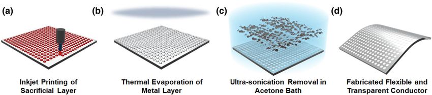
www.nature.com/scientificreports/

                                            Figure 1.  Schematic illustration for the fabrication procedure of a transparent electrode with a negative pattern
                                            of an inkjet-printed dot array. (a) PR ink-jet printing on the glass; (b) thermal evaporation of aluminum; (c) the
                                            removal of the printed PR array; (d) the metal grid electrode.

                                            the electrode within the device is facing the user, such as in a display application. To reduce its visibility to the
                                            naked eye, the line width should be less than 20 um, which is the minimum resolution of the human eye. Elec-
                                            trohydrodynamic (EHD) jet printing has also been studied to secure a narrow line width. This process provides
                                            a higher resolution than conventional inkjet printing by supplying voltage to the nozzle to form a strong electric
                                            field to print the solution. Jang et al.23 presented an invisible electrode by EHD jet printing with a line width less
                                            than 10 um. It was difficult to used at an industrial level in early stage because it is hard to maintain stable jetting
                                            condition under extremely high electric field between the nozzle and stages. In recent years, many researchers
                                            including Chen et al.24 and Khan et al.25 conducted an EHD study using multi-nozzle instead of single-nozzle.
                                            They developed the multi-nozzle printing system by restricting possible interference between electric fields by
                                            the voltage supplied to the nozzles. Likewise, the development of the fabrication process in large scale is being
                                            required in wide industrial area which is concerned with the flexible and transparent electrode.
                                                In this study, we employed a transparent and flexible electrode using a negative pattern on an inkjet-printed
                                            dot array. The dot array pattern was fabricated using inkjet printing as a sacrificial layer. By removing the sac-
                                            rificial layer, the metal layer deposited onto the sacrificial layer was removed together with the pattern of the
                                            punched hole array. This fabrication method is free from the line width limitation that enables invisibility to
                                            naked eye. Furthermore, using aluminum as the metal material instead of a noble metal significantly reduces
                                            the cost. The optical and electrical properties of the fabricated electrode were investigated by adjusting the drop
                                            distance and pattern array in the transparent electrode. Finally, the touch screen panel was made with the resis-
                                            tive type using the transparent electrode, which we successfully demonstrated.

                                            Methods
                                            The polyethylene naphthalate (PEN) substrate was prepared for inkjet printing of the sacrificial layer. The sub-
                                            strate was cleaned thoroughly using ultrasonic sonication with acetone, isopropanol, and distilled water for
                                            30 min respectively. After that, the ultraviolet surface treatment was performed for 20 min to improve adhesion
                                            between the ink and substrates. The detailed fabrication process of the transparent electrode is illustrated in
                                            Fig. 1. The ink was made by mixing a positive photoresist (PR) (az4330, AZ Electronic Materials) and its thinner
                                            (az1500, AZ Electronic Materials) with a 1:1 volume ratio using a voltex mixer. The blended solution has a viscos-
                                            ity of 9.15 cp at 24 °C and a surface tension 21.62 mN/m. A commercial inkjet printing system (Dimatix-2800,
                                            Dimatix) was used to fabricate a droplet array pattern. Each jetting of solution ink was maintained to a constant
                                            10 pl using a cartridge head (DMP-11610, Dimatix) with a 19 um nozzle diameter. The nozzle voltage was
                                            adjusted within 28 ~ 31 V and the jetting frequency is 1 kHz. After being printed, the sample was baked at 110 °C
                                            for 80 s to increase adhesion between the substrate and sacrificial layer. The sample was exposed to extreme
                                            ultraviolet for 20 s. Then, 100 nm of aluminum was deposited on the sacrificial layer with thermal evaporation.
                                            Finally, the sacrificial layer was immersed in acetone and removed using ultrasonication for 20 min. Through the
                                            removal process of the sacrificial layer, the aluminum was patterned in the punched shape from the dot array.

                                            Results
                                            The transparent electrode with a negative pattern of an inkjet-printed sacrificial dot array was fabricated with
                                            different array patterns and dot distances. The electrode was designed with two different arrays, a triangular array
                                            and a square array as explained in Fig. 2a,b. The drop spacing of the two array pattern varied from 75 to 200 um.
                                            The size of the printed droplets was consistently 67 um over the entire fabricated electrode. By decreasing the
                                            drop spacing, the width of the negative pattern could be decreased. For example, at 75 um drop spacing of the
                                            smallest distance, the width of the negative pattern was 8 um at the narrowest region. Since the negative region
                                            rather than the printed region was used, the width of the pattern could be decreased to make it narrower than
                                            the transparent part to the naked eye. Figure 2c–h present the optical microscope images of the fabricated trans-
                                            parent electrode in triangular and square shapes with 75 um, 100 um, and 150 um, respectively. The aluminum
                                            layer was colored light and the punched hole array was colored dark because the metal electrode reflected the
                                            incident light from the top. The hole pattern was formed precisely with the commercial inkjet system for printed
                                            electronics. The drop spacing could not be decreased more than 75 um because the printed drop was connected
                                            at a drop spacing of less than 75 um.
                                                The fabrication steps of the transparent electrodes were studied through an optical microscope and atomic
                                            force microscopy (AFM). Figure 3 shows the steps of the fabrication process that corresponds to Fig. 1a,b,d.

          Scientific Reports |   (2022) 12:1572 |                 https://doi.org/10.1038/s41598-022-05312-w                                                      2

Vol:.(1234567890)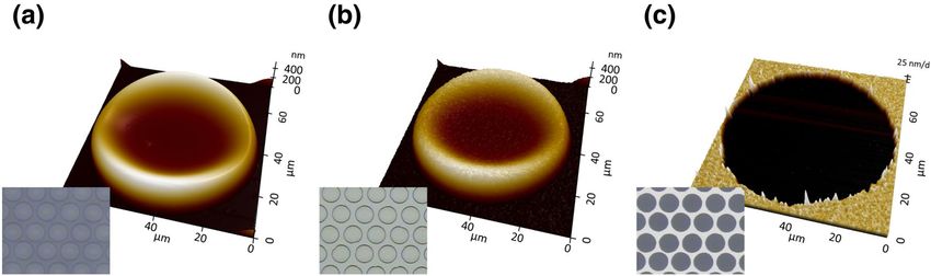
www.nature.com/scientificreports/

                                  Figure 2.  Pattern structure of the fabricated transparent electrodes with different patterning arrays and drop
                                  distances using a 67 um droplet. Schematic of the pattern shape that is connected by adjacent drop distances:
                                  (a) triangular shape, (b) square shape. Optical images by different droplet distances (c–d) 75 um, (e–f) 150 um,
                                  (g–h) 200 um.

                                  Figure 3.  AFM images and microscope images (inset) of the single unit pattern at each step: (a) inkjet printing
                                  of the PR, (b) thermal evaporation of aluminum, and (c) removal of the sacrificial layer.

                                  Figure 3a is an optical image of the patterned PR by ink-jet printing and an AFM image measuring the droplet
                                  shape of one of the patterns. There was a height difference in a printed droplet, which is known as the coffee ring
                                  effect because the shape is similar to a coffee stain mark. The coffee ring effect was formed from the difference
                                  in the relative evaporation rates of solvents during ink-jet printing.26 Since the evaporation rates of the printed
                                  ink at the outside was higher than that of the ink at the inside, the height of the edge was higher than that of the
                                  center. The ink used for the printing of the sacrificial layer also exhibited the conventional characteristics of the
                                  coffee ring effect. The maximum height of the edge area was 555 nm and the height of the center was 112 nm.
                                  After the sacrificial layer was printed, aluminum was deposited using thermal evaporation. One hundred nm of
                                  aluminum was deposited on the whole region of the printed sample, both for the sacrificial layer region and the
                                  bare substrate region. The study confirmed that the optical image was bright in the microscope image of Fig. 3b.
                                  The printed pattern followed the profile of the sacrificial layer with a concave center area. The aluminum elec-
                                  trode with a negative pattern dot array was fabricated by removing the underneath sacrificial layer. The patterned
                                  droplets were neatly removed by sonication in acetone, resulting in a transparent electrode with a negative pat-
                                  tern, as shown in Fig. 3c. The removal of the aluminum layer with the pattern of the underneath sacrificial layer
                                  was similar to the liftoff process in conventional lithography. In a general liftoff process, the thickness of the PR
                                  should be 3 ~ 4 times thicker than that of the metal layer because the height difference by the photoresist should
                                  be high enough to break the metal bonding. Though the thickness of the inkjet-printed sample was similar to
                                  the aluminum layer, the negative pattern was formed clearly and was attributed to the coffee-ring effect. Since
                                  the thickness of the edge was about 5 times higher than the center, the printed sacrificial layer gained the effect
                                  of a layer thick enough to break the metal bonding.
                                      We measured the adhesion strength of the transparent electrode fabricated by tape test. Figure S1 shows that
                                  there was little change within 19 Ω/□ during peeling. Therefore, it confirmed that the adhesion between the
                                  substrate and the deposited aluminum was very good. Abrasive resistance test helps ensure that the material’s
                                  original structure and look are maintained. We measured the friction coefficient according to the distance by
                                  applying a load of 1 N and a speed of 1 cm/s through the Ball-on-Disc method. Through Figure S2, it was con-
                                  firmed that the friction force of the fabricated transparent electrode was 0.947 N.

Scientific Reports |   (2022) 12:1572 |                https://doi.org/10.1038/s41598-022-05312-w                                                    3

                                                                                                                                                Vol.:(0123456789)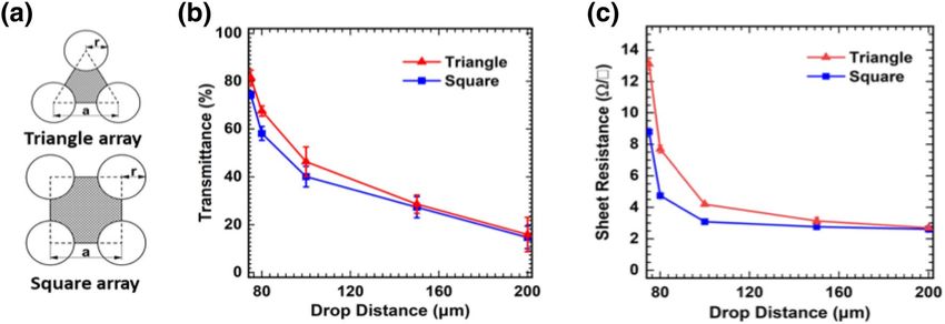
www.nature.com/scientificreports/
Figure 4. (a) Schematic illustration of the areal density of the aluminum area in the triangular and square array.
(b) Transmittance at 550 nm of wavelength and (c) sheet resistance of the fabricated transparent electrode by
drop distance with different drop pattern array.
Figure 4 shows the transmittance and the sheet resistance of the fabricated transparent electrode by the
drop distance with the triangular and square array. The transmittance of the transparent electrode is gradually
enhanced when the drop distance is decreased from 200 to 75 um, due to the decrease of the aluminum pattern
area where the incident light was reflected. When the drop distance was 75 um, the maximum transmittance with
a triangular array and square array achieved 81.4% and 74.4%, respectively. The optical properties are dependent
upon the areal density of triangular and square arrays, which can be defined as the ratio of the aluminum area
to the triangular and square areas. The areal density is expressed as:
2πr 2
(1)
Triangle array Areal density = 1 − √
3a2
πr 2
(2)
Square array Areal density = 1 − 2
a
where r is the drop radius, and a is the drop distance, as described in Fig. 4a. From the comparison of Eqs. (1)
and (2), we estimated that the triangular array with a lower aluminum areal density had a higher transmittance
than the square array. Comparing the calculated opening area with the measured transmittance, they exhibited
similar tendency but they were not entirely consistent. It might attribute to a cause from the process to pattern
the metal layer, there is inevitably over-etching or some error in the gap between the printed droplets.
Furthermore, the sheet resistance was also affected by the aluminum area density variation. As show in Fig. 4c,
the sheet resistance gradually decreased, which increased the aluminum grid drop distance. Figure 4b,c indicate
that the electrical conductivity and the transmittance had a trade-off relationship. An increase in the drop spacing
created an increase in areal density, which increased the electrical conductivity and decreased the transmittance.
From the same point of view, the sheet resistance of the square array was lower than that of the triangular array.
Not only the drop distance, the characteristics of the electrode was also determined by the thickness. Figure S3
shows the transmittance and sheet resistance of the transparent electrode with various thicknesses. The aluminum
pattern with the thickness higher than 100 nm was not achieved because the thickness is too thick to break the
films along the topography of the printed PR. On the other hands, the transparent electrode with the thickness
smaller than 100 nm exhibited small correlation with transmittance and large correlation with sheet resistance.
Though the transmittance depends on the areal density of aluminum which was determined by not the thick-
ness but electrode pattern, sheet resistance strongly depended on the thickness of the film. The decrease in the
sheet resistance is more substantial compare with the decrease transmittance. The FoM as expressed in Eq. (3)
is inversely proportional to the sheet resistance, confirming that the FoM improved as the thickness increased.
The total transmittance (T) of the fabricated transparent electrode formed by the triangular and square array
with 75 um drop spacing at wavelengths from 300 to 1000 nm is shown in Fig. 5. The samples with the other
drop spacings were also measured as shown in Figure S1. The measurement area covered total 0.5 cm by 1 cm
in area and there was negligible difference at repetitive measurements. The measurement was conducted with
the setting based on the PEN film so transmittance of the PEN film was neglected. All of the samples exhibited
the characteristics of uniform transmittance regardless of the wavelength, and the fabricated transparent elec-
trode with the triangular and square array showed transmittances of T 400 = 81.1%, T900 = 80.6%, S400 = 74.0% and
S900 = 73.8%. The other measurement results with drop distances from 80 to 200 um are given in Figure S4, which
also exhibits the uniform transmittance. Moreover, the transmittance in the visible range was slightly lower than
that of conventional ITO, but the UV area transparent electrodes still had a high transmittance unlike ITO where
light absorption occurred, which indicated that the fabricated transparent electrode had a broad transmittance
spectrum. These characteristics are advantageous in optoelectronic devices because the electrodes do not deform
the spectrum. The fabricated transparent electrode could also be used in optoelectronic devices in the ultraviolet
(UV) and infrared (IR) regions as well as the visible region.
Scientific Reports | (2022) 12:1572 | https://doi.org/10.1038/s41598-022-05312-w 4
Vol:.(1234567890)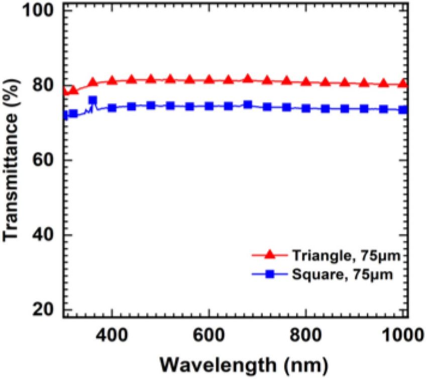
www.nature.com/scientificreports/
Figure 5. Total transmittance spectra of the fabricated transparent electrode with a 75 um drop distance.
Figure 6. Figure-of-merit values of the fabricated transparent electrode compared with other types from the
literature (ITO25,26, Ag NW28–30, CNT31,32, PEDOT:PSS33, Ag grid34, Graphene31) for comparison.
In general, transmittance and electrical conductivity has a trade-off relationship. To evaluate the fabricated
electrode properly considering the relationship, the figure-of-merit (FoM) values were calculated. An evaluation
index that included the transmittance and the sheet resistance, the FoM, was firstly suggested by H aacke27 as in
Eq. (3) where T is the optical transmittance at a wavelength of 550 nm and RS is the sheet resistance (Ω sq−1).
T 10
FoM = (3)
Rsheet
Figure 6 shows the relationship between the transmittance and the FoM of the fabricated transparent elec-
trode. The FoM increased with an increasing transmittance; in other words, by decreasing the drop spacing.
The maximum FoM was obtained at the minimum drop spacing of 75 um and the FoM of the electrode with a
triangular array was 9.7 × 10⁻³ and that with a square array was 5.9 × 10⁻³. The FoM of the triangular array and that
of the square array had the same relationship and the FoM was determined by the transmittance regardless of the
array pattern. The calculated FoM was also compared with other materials for transparent electrodes. I TO28–30,
AgNWs31–33, CNT34,35, PEDOT:PSS36, Ag g rid37, Graphene34 were selected for the comparison that was suggested
in both the literature and for commercial products. The fabricated transparent electrode exhibited comparable
values of FoM with the fabricated electrode at over 80% of transmittance. Though the transparent electrode
was fabricated using a very simple method, the performance was on a high level that brought the advantages of
low fabrication cost. Furthermore, it required a small material cost and did not need expensive nanomaterials
Scientific Reports | (2022) 12:1572 | https://doi.org/10.1038/s41598-022-05312-w 5
Vol.:(0123456789)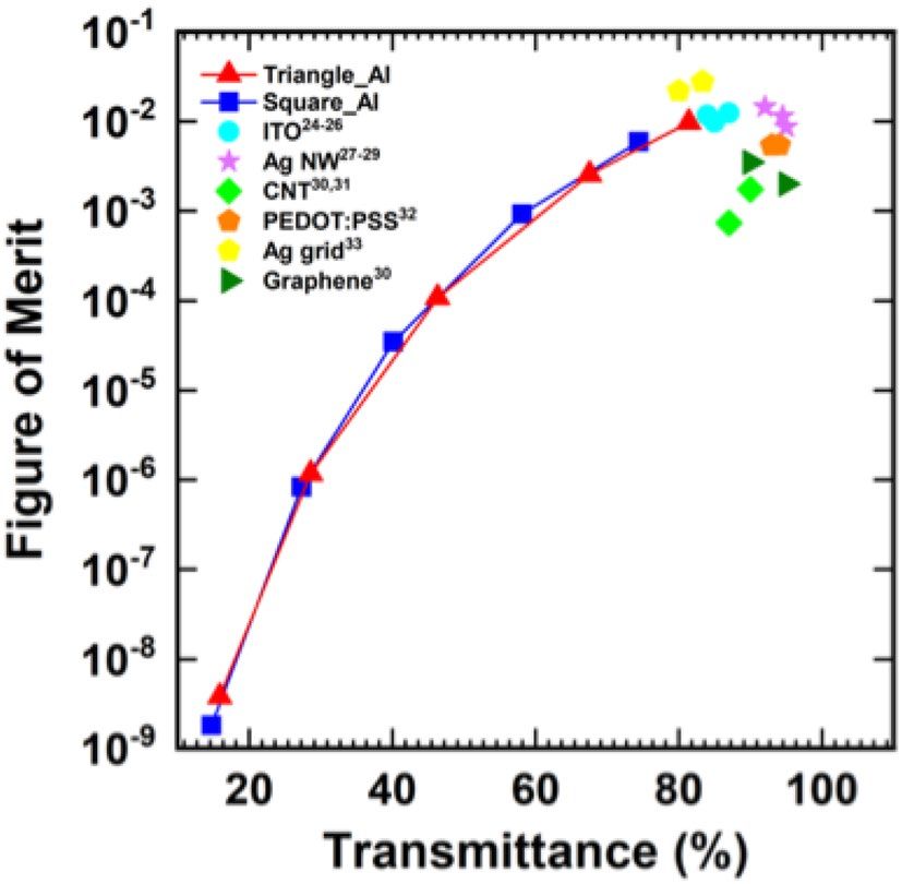
www.nature.com/scientificreports/
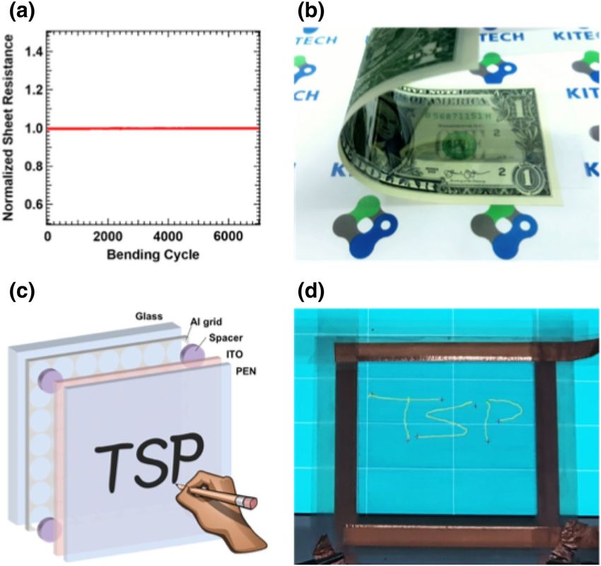
Figure 7. (a) Measured normalized sheet resistance during the mechanical bending test with a 5 mm bending
radius. (b) Flexible transparent electrode demonstrated on a one-dollar bill. (c) Schematic illustration of a touch
screen panel (TSP) (d) TSP operation on an LCD screen. “TSP” was written on TSP.
such as AgNWs, CNT, and graphene. The required amount of the photoresist for printing of the sacrificial layer
was also small because the drop array was patterned with a drop-on-demand method with a high edge height.
To determine the mechanical flexibility of the fabricated Al electrode, the electrode was folded back and forth
with a bending radius of 9 mm to 0.5 mm, and its resistance was compared to its initial value. The resistance of
the Al grid mesh electrode remained stable up to a bending radius of 1 mm, which indicates that the transpar-
ent electrode has excellent mechanical flexibility. The electromechanical reliability of the fabricated transpar-
ent electrode was plotted in Fig. 7a by measuring the normalized sheet resistance during the cyclic bending
test. The test was performed with 1 Hz of repetition rate and 5 cm by 5 cm of sample size. The resistance was
measured frequently with the rate of 4 times per cycle. There was little change within 1% during the 7000 cycles
of the bending test. The electrode guaranteed the mechanical robustness against bending fatigue. In addition,
we conducted bending tests on commercial ITO/PEN electrodes for further comparison. The resistance of the
ITO/PEN electrode increased rapidly according to bending cycles, as shown Figure S5. These properties show a
contrast in flexibility with our fabricated electrodes. Figure 7b shows the flexible electrode that was attached on
the center of a one-dollar bill to exhibit its flexibility. The electrode has undergone cyclic bending test, and the
normalized resistance of the electrode after each cycle in the relaxed state was plotted in Fig. 7a. The region of
the transparent electrode could be seen at a slightly darker region of the bill rather than at the outside edges. A
touch-screen panel (TSP) was demonstrated and is shown in Fig. 7c,d. The pattern of the triangular array with a
75 µ m drop spacing was selected for the demonstration. Figure 7c shows a schematic illustration for the demon-
stration of a four-wire resistive touch-screen panel. The TSP consists of the fabricated transparent electrode and
the counter electrode of ITO deposited on a PEN substrate. While having the spacers in between these electrodes,
the top conducting layer for resistive touch screen panel must be flexible because a mechanical pressure should
be regularly applied, and the bottom electrode can be either rigid or flexible. ITO-PEN film is used as a counter
electrode with comparable sheet resistance. The size of each drop pattern was 67 mµ for the substrate and the
area of the fabricated transparent electrode was 10 cm × 8 cm. The resistive touch panel detects a position of a
touch by capturing the electrical resistance at the point of contact where an electrical short is created. The copper
tapes are applied at both ends of each conductor and properly insulated to measure accurate detection of touch.
The function of the produced TSP was confirmed by writing the letters “TSP” on the screen. The letters were
accurately recognized on the screen by detecting touch pressure on the fabricated TSP.
TSP was successfully demonstrated by using the fabricated transparent electrode with patterned aluminum
thin film despite of the roughness of the electrode. The gap between the upper and lower electrode was far from
Scientific Reports | (2022) 12:1572 | https://doi.org/10.1038/s41598-022-05312-w 6
Vol:.(1234567890)www.nature.com/scientificreports/
the On the other hand, the non-uniform thin film might be disadvantages to the devices with the structure of
stacked thin film such as thin film solar c ells38,39 and light emitting d
iodes40,41. The roughness of the electrodes
might result in electrical nonuniformity and leakage current sometimes in severe cases. The lack of flatness was
remained as further issue to expand its usability. Meanwhile, this fabrication process had advantages in wide
choice for the material. The experiments in this study choose the PR because it was easy to control the viscosity to
be within the printable range. The selected solution was also clearly removed by the ultrasonication process with
immersed in acetone. Therefore, if the solution satisfies these two conditions, any other commercial materials can
be employed in this study. Not only the sacrificial material, metal for the thin film also be in wide choice such as
copper as well as aluminum. The variability of the solution selection is one of great advantages on our studies.
Discussion
A flexible transparent electrode was fabricated by patterning aluminum thin film though an inkjet-printed sac-
rificial layer. With this process, a metal grid electrode can be produced simply by inkjet-printing and thermal
evaporation without a shadow mask. Furthermore, many kinds of material, including metallic and inorganic
elements, can be used with this method, which expands its application. This facile fabrication method enabled
fine patterning of the electrode with a width of less than 10 um, which is less than the visibility of the naked eye.
Unlike the commercial ITO, it can be used in the UV region or IR region as well as the visible region. The figure-
of merit, defined to optimize the transmittance and sheet resistance, was comparable to the other materials as
candidates for flexible transparent electrodes. This transparent electrode also exhibited an excellent stability in
any mechanical stress, including bending. Finally, a touch screen panel was demonstrated to confirm the poten-
tial of the transparent electrode on versatile applications. This work, including the new fabrication technology
with a mask-less process for transparent electrodes, will provide new insights for the further development of
thin film electronics.
Received: 3 September 2021; Accepted: 29 December 2021
References
1. An, K. et al. Germinant ZnO nanorods as a charge-selective layer in organic solar cells. J. Mater. Sci. Technol. 55, 89–94 (2020).
2. Mortimer, R. J., Dyer, A. L. & Reynolds, J. R. Electrochromic organic and polymeric materials for display applications. Displays
27, 2–18 (2006).
3. Wu, H. et al. A transparent electrode based on a metal nanotrough network. Nanotechnology 8, 421–425 (2013).
4. Bae, E. J., Kang, Y. H., Lee, C. & Cho, S. Y. Engineered nanocarbon mixing for enhancing the thermoelectric properties of a
telluride-PEDOT:PSS nanocomposite. J. Mater. Chem. A 5, 17867–17873 (2017).
5. Paeng, D. et al. Low-cost facile fabrication of flexible transparent copper electrodes by nanosecond laser ablation. Adv. Mater. 27,
2762–2767 (2015).
6. Hecht, D. S., Hu, L. & Irvin, G. Emerging transparent electrodes based on thin films of carbon nanotubes, graphene, and metallic
nanostructures. Adv. Mater. 23, 1482–1513 (2011).
7. Leem, D.-S. et al. Efficient organic solar cells with solution-processed silver nanowire electrodes. Adv. Mater. 23, 4371–4375 (2011).
8. Zhang, Y. et al. Polymer-Embedded carbon nanotube ribbons for stretchable conductors. Adv. Mater. 22, 3207–3031 (2010).
9. Pang, S., Hernandez, Y., Feng, X. & Müllen, K. Graphene as transparent electrode material for organic electronics. Adv. Mater. 23,
2779–2795 (2011).
10. Zhou, Y. et al. Inverted and transparent polymer solar cells prepared with vacuum-free processing. Soalr Energy Materials & Solar
Cells. 93, 497–500 (2009).
11. Sahu, D. R., Lin, S.-Y. & Huang, J.-L. ZnO/Ag/ZnO multilayer films for the application of a very low resistance transparent electrode.
Appl. Surf. Sci. 252, 7509–7514 (2006).
12. Cao, W. et al. Flexible organic solar cells using an oxide/metal/oxide trilayer as transparent electrode. Org. Electron. 13, 2221–2228
(2012).
13. Kim, Y. C. et al. Optimization and device application potential of oxide–metal–oxide transparent electrode structure. RSC Adv. 5,
65094–65099 (2015).
14. Hong, S. et al. Nonvacuum, maskless fabrication of a flexible metal grid transparent conductor by low-temperature selective laser
sintering of nanoparticle ink. ACS Nano 7, 5024–5031 (2013).
15. Schneider, J. et al. Electrohydrodynamic nanodrip printing of high aspect ratio metal grid transparent electrodes. Adv. Funct.
Mater. 26, 833–840 (2016).
16. Guillorn, M. A., Carr, D. W., Tiberio, R. C., Greenbaum, E. & Simpson, M. L. Fabrication of dissimilar metal electrodes with
nanometer interelectrode distance for molecular electronic device characterization. J. Vac. Sci. Technol. B. 18, 1177 (2000).
17. Zou, J., Yip, H.-L., Hau, S. K. & Jen, A.K.-Y. Metal grid/conducting polymer hybrid transparent electrode for inverted polymer
solar cells. Appl. Phys. Lett. 96, 203301 (2010).
18. Spechler, J. A. & Arnold, C. B. Direct-write pulsed laser processed silver nanowire networks for transparent conducting electrodes.
Appl. Phys. A. 108, 25–28 (2012).
19. Liu, Y.-H. et al. High-performance, ultra-flexible and transparent embedded metallic mesh electrodes by selective electrodeposi-
tion for all-solid-state supercapacitor applications. J. Mater. Chem. 5, 9032–9041 (2017).
20. Shin, K.-Y., Hong, J.-Y. & Jang, J. Flexible and transparent graphene films as acoustic actuator electrodes using inkjet printing.
Chem. Commun. 47, 8527–8529 (2011).
21. Layani, M. et al. Nanostructured electrochromic films by inkjet printing on large area and flexible transparent silver electrodes.
Nanoscale 6, 4572–4576 (2014).
22. Secor, E. B., Prabhumirashi, P. L., Puntambekar, K., Geier, M. L. & Hersam, M. C. Inkjet printing of high conductivity, flexible
graphene patterns. J. Phys. Chem. Lett. 4, 1347–1351 (2013).
23. Jang, Y., Kim, J. & Byun, D. Invisible metal-grid transparent electrode prepared by electrohydrodynamic (EHD) jet printing. J.
Phys. D: Appl. Phys. 46, 155103 (2013).
24. Chen, M. et al. Parallel, Multi-Material Electrohydrodynamic 3D Nanoprinting. Small 16, 190640 (2020).
25. Khan, A. et al. Fabrication of circuits by multi nozzle electrohydrodynamic inkjet printing for soft wearable electronics. J. Mater.
Res. 36, 3568–3578 (2021).
Scientific Reports | (2022) 12:1572 | https://doi.org/10.1038/s41598-022-05312-w 7
Vol.:(0123456789)www.nature.com/scientificreports/
26. Yunker, P. J., Still, T., Lohr, M. A. & Yodh, A. G. Suppression of the coffee-ring effect by shape-dependent capillary interactions.
Nature 476, 308–311 (2011).
27. Haacke, G. New figure of merit for transparent conductors. J. Appl. Phys. 47, 4086–4089 (1976).
28. BIOTAIN Crystal, Longyan City, China, http://www.crystal-material.com/.
29. SCIST ITO, Suwon, Korea, https://scist.co.kr/.
30. Luminescence Technology Corp, Seongnam, Korea, https://www.lumtec.com.tw/.
31. Novarials, Woburn, MA, https://www.novarials-store.com/.
32. Kwon, J. et al. Recent progress in silver nanowire based flexible/wearable optoelectronics. J. Mater. Chem. C. 6, 7445–7461 (2018).
33. Yi, P., Zhu, Y. & Deng, Y. Fabrication and applications of flexible transparent electrodes based on silver nanowires (InTech, Avail-
able from: https://doi.org/10.5772/intechopen.77506, 2018)
34. Sohn, H., Park, C., Oh, J.-M., Kang, S. W. & Kim, M.-J. Silver nanowire networks: Mechano-electric properties and applications.
Materials. 12, 2526 (2019).
35. Kim, T. H. et al. An active carbon-nanotube polarizer-embedded electrode and liquid-crystal alignment. Nanoscale 12, 17698–
17702 (2020).
36. Dauzon, E. et al. Stretchable and transparent conductive PEDOT:PSS-based electrodes for organic photovoltaics and strain sensors
applications. Adv. Funct. Mater. (2020)
37. Choi, B. S., Choi, S. H., Ryu, J. H. & Cho, H. Comparison of characteristics of silver-grid transparent conductive electrodes for
display devices according to fabrication method. J. Korean Cryst. Growth Cryst. Technol. 27, 75–79 (2017).
38. Lee, J. et al. A dual-scale metal nanowire network transparent conductor for highly efficient and flexible organic light emitting
diodes. Nanoscale 9, 1978–1985 (2017).
39. Kim, J. Y. et al. Universal elaboration of al-doped tio2 as an electron extraction layer in inorganic-organic hybrid Perovskite and
organic solar cells. Adv. Mater. Interfaces 7, 1902003 (2020).
40. An, K., Yoon, D. G. & Kang, K.-T. Effects of residual solvent in printed phosphorescent emissive thin films as, the origin of limited
efficiency in organic light emitting diodes. Progr. Org. Coat. 147, 105781 (2020).
41. Han, Y. J., An, K., Kang, K. T., Ju, B.-K. & Cho, K. H. Optical and electrical analysis of annealing temperature of high-molecular
weight hole transport layer for quantum-dot light-emitting diodes. Sci. Rep. 9(1), 10385 (2019).
Acknowledgements
This study was conducted with the support of the Korea Institute of Industrial Technology as "Development of
root technology for multi-product flexible production (KITECH EO-21-0008)". This research was supported by
the Basic Science Research Program through the National Research Foundation of Korea (NRF) funded by the
Ministry of Education (NRF-2021R1I1A3059714).
Author contributions
C.K. and K.A. wrote the main manuscript text and Mingu Kang did a inkjet experiment. P.W. and J.-J.P. prepare
Fig. 7. All authors reviewed the manuscript.
Competing interests
The authors declare no competing interests.
Additional information
Supplementary Information The online version contains supplementary material available at https://doi.org/
10.1038/s41598-022-05312-w.
Correspondence and requests for materials should be addressed to B.-K.J. or K.-T.K.
Reprints and permissions information is available at www.nature.com/reprints.
Publisher’s note Springer Nature remains neutral with regard to jurisdictional claims in published maps and
institutional affiliations.
Open Access This article is licensed under a Creative Commons Attribution 4.0 International
License, which permits use, sharing, adaptation, distribution and reproduction in any medium or
format, as long as you give appropriate credit to the original author(s) and the source, provide a link to the
Creative Commons licence, and indicate if changes were made. The images or other third party material in this
article are included in the article’s Creative Commons licence, unless indicated otherwise in a credit line to the
material. If material is not included in the article’s Creative Commons licence and your intended use is not
permitted by statutory regulation or exceeds the permitted use, you will need to obtain permission directly from
the copyright holder. To view a copy of this licence, visit http://creativecommons.org/licenses/by/4.0/.
© The Author(s) 2022
Scientific Reports | (2022) 12:1572 | https://doi.org/10.1038/s41598-022-05312-w 8
Vol:.(1234567890)You can also read