Vis and NIR Diffuse Reflectance Study in Disordered Bismuth Manganate-Lead Titanate Ceramics

Page created by Daniel Yates
 
CONTINUE READING
Vis and NIR Diffuse Reflectance Study in Disordered Bismuth Manganate-Lead Titanate Ceramics
electronic materials

Article
Vis and NIR Diffuse Reflectance Study in Disordered Bismuth
Manganate—Lead Titanate Ceramics
Andrzej Molak * , Anna Z. Szeremeta and Janusz Koperski

                                          August Chełkowski Institute of Physics, University of Silesia in Katowice, ul. 75 Pułku Piechoty 1,
                                          41-500 Chorzów, Poland; anna.szeremeta@us.edu.pl (A.Z.S.); janusz.koperski@us.edu.pl (J.K.)
                                          * Correspondence: andrzej.molak@us.edu.pl; Tel.: +48-32-3497638

                                          Abstract: This work shows a correlation between light reflectance, absorption, and morphologies of
                                          series of bismuth manganate–lead titanate, (1 − x) BM–x PT, (x = 0.00, 0.02, 0.04, 0.08, 0.12, 0.16, 0.24,
                                          1.00) ceramics composite. Low reflectance in the Vis-NIR range corresponds to ‘black mirror’ features.
                                          The modified Kubelka-Munk function applied to measured visible-near infrared (Vis-NIR) diffuse
                                          reflectance enabled the estimation of the energy gaps magnitude of the order of 1.0–1.2 eV for BM-PT.
                                          Histograms of grains, obtained using a scanning electron microscope, enabled finding the correlation
                                          between grains size, reflectance magnitude, and PT content. The magnitude of energy gaps was
                                          attributed to electronic structure bands modified by crystal lattice disorder and oxygen vacancies.

                                          Keywords: bismuth manganate; ceramics composite; lead titanate; energy gap; surface morphology;
                                          Vis-NIR reflectance

                                1. Introduction
         
                                               Perovskite ABO3 oxide materials attract attention for solar cells research and devel-
Citation: Molak, A.; Szeremeta, A.Z.;
                                          opment and photovoltaic studies. The energy gap, Egap , which separates the energies of
Koperski, J. Vis and NIR Diffuse
                                          the valence band, VB, maximum, and conduction band minimum, determines the material
Reflectance Study in Disordered
Bismuth Manganate—Lead Titanate
                                          possibilities for such applications [1]. Electronic structure tuning is necessary for many
Ceramics. Electron. Mater. 2022, 3,
                                          materials to obtain suitable optical Egap demanded for optical applications. The power
101–114. https://doi.org/10.3390/         conversion high efficiency also depends on the long lifetimes of excited charge carriers,
electronicmat3010010                      which allows travel across long distances prior to recombination. Moreover, in accord
                                          to the Shockley–Queisser limit, the highest efficiency is reached at a band gap energy of
Academic Editor: Jai Singh
                                          1.34 eV [2,3].
Received: 28 October 2021                      The ABO3 VB is formed by oxygen O 2p states hybridized with states of metal 3d, 4d,
Accepted: 17 February 2022                and 5d placed in the B position. The 4d and 5d metal ions placed in B sublattice usually
Published: 25 February 2022               form a wide gap in the electronic structure. For instance, several perovskite titanates
                                          and niobates show insulator Egap of the order of 3 eV and ultraviolet, UV, light range
Publisher’s Note: MDPI stays neutral
                                          only is available for energy harvesting, due to limited light absorption in Vis range. It
with regard to jurisdictional claims in
published maps and institutional affil-
                                          is worth noting that the light energies higher than the Vis-UV limit are insufficient for
iations.
                                          photovoltaic applications.
                                               The wide gap ferroelectric perovskites provide low electrical conductivity and negligi-
                                          ble dielectric losses. Moreover, it should be noticed that ferroelectric ordering enhances
                                          absorption efficiency due to empty d0 shells crucial for the formation of the ferroelectric
Copyright: © 2022 by the authors.         state, which exerts a weak force on the moving charge carriers. Simultaneously, when
Licensee MDPI, Basel, Switzerland.        the electron-hole pairs are formed after photon absorption, the electrons and holes can
This article is an open access article    be separated and pushed towards opposite directions by the electric fields of the internal
distributed under the terms and           polarization [4–6].
conditions of the Creative Commons             Contrary, the narrow band perovskites can be obtained from the oxides of the metal
Attribution (CC BY) license (https://     ions from the 3d group, e.g., Fe, Mn, Cr, and Co. They offer better ability, including
creativecommons.org/licenses/by/          absorption in Vis and NIR, range. However, narrow optical Egap results in low activation
4.0/).

Electron. Mater. 2022, 3, 101–114. https://doi.org/10.3390/electronicmat3010010                           https://www.mdpi.com/journal/electronicmat
Vis and NIR Diffuse Reflectance Study in Disordered Bismuth Manganate-Lead Titanate Ceramics
Electron. Mater. 2022, 3                                                                                               102

                           energy in electric conductivity, which induces marked electrical cross-current flow and
                           losses [7–19].
                                 There are several routes to modify the optical Egap of oxide ABO3 materials. De-
                           manded properties can be obtained when materials exhibiting different Egap magnitude
                           are combined. Consequently, composites formed from oxide materials, which show large
                           and narrow Egap , respectively, allow modifying the optical properties because the narrower
                           gap may enhance light absorbance efficiency in the Vis-NIR range. The substitution of
                           the metal ions can lead either to solid solutions or the formation of precipitates. Minor
                           phases may appear when the solubility limit is overstepped, and/or a transformation of
                           the phases occurs [15,20]. The electronic structure can also be modified by an additional
                           treatment that can change the concentration of the oxygen vacancies, V O defects [21–23].
                           The V O forms shallow and deep energy levels within the Egap , increasing both absorbance
                           at lower energies and electrical losses [24]. For instance, the active role of the Mn2+ /Mn3+
                           in capturing photons in the NIR spectrum in the case of, e.g., multilayer Bi(Fe1−x Mnx )O3
                           photonic crystals and Mn-doped TiO2 was analyzed [20,25–27].
                                 From such points of view, narrow gap manganates and wide gap ferroelectric per-
                           ovskites attract attention for photovoltaic applications [6,17,20,28]. In our study, we have
                           chosen BM and PT to obtain ceramics composite. We presumed that ferroelectric PT
                           addition to semiconductor BM would affect the electronic structure and influence light
                           reflectance and absorption efficiency.
                                 The PT shows a tetragonal P4mm phase at room temperature. Ferroelectric-paraelectric
                           phase transition, which occurs in 763 K, points to the high stability of this compound
                           ferroelectric phase. PT crystal is the ferroelectric insulator showing measured optical
                           Egap = 3.4 eV [29–31]. The tuning of the energy gap was achieved by defects and doping
                           control. The Mn-doped PT crystals exhibited optical Egap lowered to 2.0–2.7 eV, attributed
                           to the occurrence of V O and dipole Mnk+ -V O defects [32]. The defected crystal, that is, N-
                           V O co-doped PT, showed the experimental Egap = 2.93 eV [29]. The PT powder, which was
                           used for the sintering of the BM-PT ceramic, was obtained from hydrothermal growth [33].
                                 BM structure depends on growth conditions [34–36]. We sintered BM ceramics in stan-
                           dard high-temperature ambient air conditions, and a thermodynamically stable two-phase
                           self-composite compound was obtained. Occurrence of two phases in equilibrium: 38% of
                           the cubic I23 with the Bi12 MnO20 composition and 62% of the orthorhombic Pbam with the
                           BiMn2 O5 composition were determined [37]. The self-composite BM was an electrically
                           non-polar compound, which exhibited antiferromagnetic order in a low-temperature range
                           with TNéel ≈ 39 K [38]. In accordance with the literature, the BiMn2 O5 phase exhibited
                           Egap = 1.24 eV for thin films [39], and Egap =1.61 eV, for nano-grain material [40]. The
                           Egap = 0.78 eV [41] and Egap = 1.23 eV [42] was calculated dependably on the modeling
                           method. The sillenite Bi12 MnO20 exhibits intrinsic Egap = 1.86 eV, intermediate band related
                           to the gap of ~1.07 eV, and VB placed 1.4 eV below the Fermi level [43]. It should be noted
                           that the Egap = 1.1 eV was estimated for the thin film perovskite BiMnO3 variance [27,44].
                           Moreover, differences in energy states related to a material’s particular phases would
                           be determined since their contribution can manifest as a superposition in the spectral
                           response [44]. Therefore, diffuse reflectance of the (1 − x) BM–x PT composite ceramics
                           should be determined in the Vis and NIR ranges of the photon spectrum.
                                 A series of (1 − x) BM–x PT, (x = 0.00, 0.02, 0.04, 0.08, 0.12, 0.16, 0.24, 1.00) ceramics
                           was sintered previously and their phases were determined using XRD, SEM, and dielectric
                           impedance tests [45–47]. In this work, we studied diffuse reflectance in the Vis-NIR range
                           to determine the PT content influence on the BM-PT composite absorption coefficient mag-
                           nitude. It should be noted that the reflectance magnitude also depends on the properties of
                           the surface exposed to the incident light. Hence, we determined ceramics’ morphology us-
                           ing scanning electron microscopy. This manuscript discusses the correspondence between
                           light reflectance, estimated absorption coefficient energy gap, ceramics’, and morphology.
Vis and NIR Diffuse Reflectance Study in Disordered Bismuth Manganate-Lead Titanate Ceramics
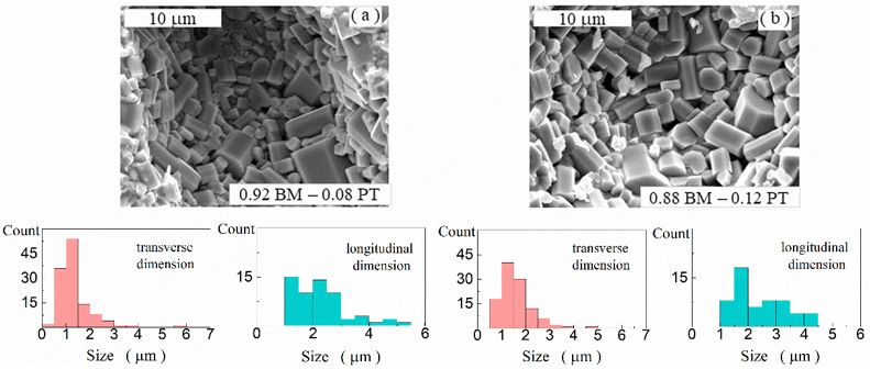
Electron. Mater. 2022, 3                                                                                                 103

                           2. Materials and Methods
                           2.1. Preparation of Composite Ceramics
                                A series of (1 − x) BM–x PT (x = 0.00, 0.02, 0.04, 0.08, 0.12, 0.16, 0.24, 1.00) ceramics was
                           produced via standard high temperature sintering. A two-stage procedure was performed.
                           BM ceramics [48] and PT powder [33] were prepared separately at the first step. BM
                           ceramics were produced using high-temperature sintering in the air (TS = 1170 K for 2 h),
                           according to the nominal BiMnO3 formula [49]. They were graphite-like in color. The
                           stoichiometric PT powder, which showed grains of sizes on submicron level (
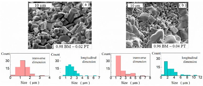
Vis and NIR Diffuse Reflectance Study in Disordered Bismuth Manganate-Lead Titanate Ceramics
Electron.
 Electron. Mater.
           Mater. 2022,
                  2022, 33, FOR PEER REVIEW                                                                                              104    4

                                   Figure 1. Secondary electron images obtained for BM ceramics (a) and PT ceramics (b). Histograms
                                   show grains’ transverse, longitudinal, and diameter size distribution.

                                        The 0.98 BM–0.02 PT ceramics (Figure 2a) shows variation in grain size similar to the
                                   pure BM ceramics. The obtained distribution shows that the grain transverse dimension
                                   is mostly between 0.5–2.5 μm. The longitudinal dimension is mostly between 0.2 and 3.5
                                   μm. There is a low number of larger grains with sizes reaching 6.5 μm. On the contrary,
                                   the 0.96 BM–0.04 PT ceramics exhibits a higher number of small grains (Figure 2b). More-
                                   over, obtained grains size distributions show an increased number of larger size grains
                                   compared to the previous composition. Namely, grain’ transverse dimension is mostly
                                   between
                                   Figure
                                    Figure 1. 1.0–5.0 μm,
                                           1. Secondary
                                              Secondary    and the
                                                        electron
                                                         electron    longitudinal
                                                                 images
                                                                  imagesobtained   dimension
                                                                          obtainedfor
                                                                                    forBM
                                                                                        BM ceramicsis mostly
                                                                                             ceramics (a)(a)
                                                                                                          and  between
                                                                                                               PT
                                                                                                             and         0.5
                                                                                                                  ceramics
                                                                                                                 PT          and
                                                                                                                           (b).
                                                                                                                    ceramics       4.0 μm.
                                                                                                                                Histograms
                                                                                                                              (b). Histograms
                                   There
                                   show   are several
                                    show grains’
                                          grains’      largelongitudinal,
                                                  transverse,
                                                 transverse,  grains withand
                                                              longitudinal,longitudinal
                                                                            anddiameter
                                                                                diameter  sizes
                                                                                            size
                                                                                         size     above 10.0 μm.
                                                                                                 distribution.
                                                                                               distribution.

                                         The 0.98 BM–0.02 PT ceramics (Figure 2a) shows variation in grain size similar to the
                                    pure BM ceramics. The obtained distribution shows that the grain transverse dimension
                                    is mostly between 0.5–2.5 μm. The longitudinal dimension is mostly between 0.2 and 3.5
                                    μm. There is a low number of larger grains with sizes reaching 6.5 μm. On the contrary,
                                    the 0.96 BM–0.04 PT ceramics exhibits a higher number of small grains (Figure 2b). More-
                                    over, obtained grains size distributions show an increased number of larger size grains
                                    compared to the previous composition. Namely, grain’ transverse dimension is mostly
                                    between 1.0–5.0 μm, and the longitudinal dimension is mostly between 0.5 and 4.0 μm.
                                    There are several large grains with longitudinal sizes above 10.0 μm.

                                   Figure 2. Secondary electron
                                   Figure                 electron images
                                                                    imagesobtained
                                                                           obtainedforfor0.98
                                                                                           0.98BM–0.02
                                                                                                BM–0.02PTPT
                                                                                                          ceramics
                                                                                                             ceramics(a)(a)
                                                                                                                         and  0.96
                                                                                                                            and    BM–0.04
                                                                                                                                 0.96      PT
                                                                                                                                      BM–0.04
                                   PT ceramics
                                   ceramics  (b).(b). Histograms
                                                  Histograms      show
                                                               show      grains’
                                                                      grains’    transverse
                                                                              transverse  andand  longitudinal
                                                                                               longitudinal sizesize distribution.
                                                                                                                 distribution.

                                          Figure 3a,b show
                                          Figure        show similar
                                                              similarmorphology
                                                                       morphologyofof0.92
                                                                                        0.92BM–0.08
                                                                                              BM–0.08  PTPT
                                                                                                          and
                                                                                                            and0.88 BM–0.12
                                                                                                                  0.88 BM–0.12PT PT
                                                                                                                                  ceram-
                                                                                                                                     ce-
                                    ics, respectively.
                                    ramics,             The The
                                             respectively.  obtained  histograms
                                                                 obtained         showshow
                                                                          histograms      that that
                                                                                               the amount   of the
                                                                                                    the amount   ofgrain’ of transverse
                                                                                                                    the grain’ of trans-
                                    variesvaries
                                    verse   between   0.3–3.0
                                                  between      µm for
                                                             0.3–3.0 μmboth
                                                                         forceramics.   The longitudinal
                                                                             both ceramics.                 dimension
                                                                                               The longitudinal          distribution
                                                                                                                  dimension            is
                                                                                                                               distribu-
                                    slightly  different  when   compared   for these two   ceramics   and  varies between
                                    tion is slightly different when compared for these two ceramics and varies between 1.0– 1.0–5.5  µm
                                    for μm
                                    5.5
Electron. Mater. 2022, 3, FOR PEER REVIEW
                                         0.92for
                                              BM–0.08    PT andPT
                                                 0.92 BM–0.08     1.0–4.5 µm forμm
                                                                     and 1.0–4.5   thefor
                                                                                       12% theof12%
                                                                                                  PT.of
                                                                                                      There  are noare
                                                                                                        PT. There    large grainsgrains
                                                                                                                       no large     with5
                                    longitudinal   size above  6.0 µm,  which  occur for  the ceramics   with a low  amount
                                    with longitudinal size above 6.0 μm, which occur for the ceramics with a low amount of    of dopant
                                    PT (compare
                                    dopant          Figures Figures
                                             PT (compare    2 and 3).2 and 3).

                                    Figure 2. Secondary electron images obtained for 0.98 BM–0.02 PT ceramics (a) and 0.96 BM–0.04
                                    PT ceramics (b). Histograms show grains’ transverse and longitudinal size distribution.

                                         Figure 3a,b show similar morphology of 0.92 BM–0.08 PT and 0.88 BM–0.12 PT ce-
                                    ramics, respectively. The obtained histograms show that the amount of the grain’ of trans-
                                    verse varies between 0.3–3.0 μm for both ceramics. The longitudinal dimension distribu-
                                    tion is slightly different when compared for these two ceramics and varies between 1.0–
                                    5.5 μm for 0.92 BM–0.08 PT and 1.0–4.5 μm for the 12% of PT. There are no large grains
                                    with longitudinal size above 6.0 μm, which occur for the ceramics with a low amount of
                                    dopant PT (compare Figures 2 and 3).

                                               Secondary electron
                                    Figure 3. Secondary    electronimages
                                                                    imagesobtained
                                                                            obtainedfor
                                                                                      for0.92
                                                                                           0.92BM–0.08
                                                                                                BM–0.08PTPT  ceramics
                                                                                                          ceramics   (a)(a)
                                                                                                                         andand
                                                                                                                             0.880.88 BM–0.12
                                                                                                                                   BM–0.12 PT
                                    PT ceramics
                                    ceramics  (b).(b). Histograms
                                                   Histograms      show
                                                                show     grains’
                                                                      grains’    transverse
                                                                              transverse  andand  longitudinal
                                                                                               longitudinal sizesize distribution.
                                                                                                                 distribution.

                                          The obtained results for the high contents of PT are shown in Figure 4a,b. We can see
                                    that the 0.84 BM–0.16 PT structure contains both large and tiny grains. The transverse size
                                    of the grain is mostly between 0.3 and 2.0 μm. Moreover, there are grains, which dimen-
                                    sions reach 7.0 μm. Grains’ longitudinal dimensions vary from 0.2 μm to 12.0 μm (Figure
Vis and NIR Diffuse Reflectance Study in Disordered Bismuth Manganate-Lead Titanate Ceramics
Electron. Mater. 2022, 3                                                                                                       105
                                    Figure 3. Secondary electron images obtained for 0.92 BM–0.08 PT ceramics (a) and 0.88 BM–0.12
                                    PT ceramics (b). Histograms show grains’ transverse and longitudinal size distribution.

                                          The obtained
                                          The  obtained results
                                                           results for
                                                                    forthe
                                                                        thehigh
                                                                            highcontents
                                                                                   contentsofofPTPTare shown
                                                                                                     are shown in in
                                                                                                                  Figure
                                                                                                                     Figure4a,b. We We
                                                                                                                              4a,b.  cancan
                                                                                                                                          see
                                    that the  0.84 BM–0.16    PT structure   contains   both  large and  tiny grains.  The  transverse
                                    see that the 0.84 BM–0.16 PT structure contains both large and tiny grains. The transverse           size
                                    of the
                                    size ofgrain   is mostly
                                             the grain        between
                                                         is mostly       0.3 and
                                                                     between    0.32.0 μm.
                                                                                     and  2.0Moreover,   there are
                                                                                               µm. Moreover,        grains,
                                                                                                                 there       which dimen-
                                                                                                                        are grains,   which
                                    sions reach 7.0
                                    dimensions         μm.7.0
                                                   reach    Grains’  longitudinal
                                                              µm. Grains’            dimensions
                                                                             longitudinal          vary from
                                                                                             dimensions       0.2from
                                                                                                           vary    μm to0.212.0
                                                                                                                            µmμm     (Figure
                                                                                                                                 to 12.0 µm
                                    4a). In turn,
                                    (Figure        theturn,
                                             4a). In    0.76the
                                                             BM–0.24    PT transverse
                                                                0.76 BM–0.24             size is mostly
                                                                                 PT transverse           between
                                                                                                 size is mostly     0.5 and0.5
                                                                                                                 between     3.0and
                                                                                                                                  μm,3.0
                                                                                                                                       while
                                                                                                                                         µm,
                                    the grains’
                                    while        longitudinal
                                           the grains’          size issize
                                                         longitudinal    between    1.0 and
                                                                             is between   1.05.5 μm5.5
                                                                                               and   (Figure  4b). 4b).
                                                                                                       µm (Figure

                                    Figure 4.
                                           4. Secondary
                                              Secondary electron
                                                          electronimages
                                                                   imagesobtained
                                                                          obtainedfor
                                                                                    for0.84
                                                                                         0.84 BM–0.16
                                                                                            BM–0.16  PTPT ceramics
                                                                                                        ceramics  (a)(a)
                                                                                                                      andand
                                                                                                                          0.760.76 BM–0.24
                                                                                                                                BM–0.24 PT
                                    PT ceramics  (b). Histograms  show grains’ transverse   and longitudinal size distribution.
                                    ceramics (b). Histograms show grains’ transverse and longitudinal size distribution.

                                          The ceramic composites studied herein exhibit many caverns in the fracture surfaces
                                     (Figure 5). Such
                                                  Such cavities
                                                        cavities are typical for the reference bismuth manganate manganate ceramics
                                                                                                                               ceramics [49].
                                                                                                                                           [49].
                                     Their
                                     Their origin
                                           origin would
                                                   would be associated with the technological process  process and attributed to chemical
                                     reactions. The
                                                 The occurrence
                                                      occurrence of these cavities, where well-formed grains are visible, is one
                                     common feature of the BM-PT ceramics. The other common feature is porosity. We can
                                     distinguish well-shaped
                                                   well-shaped hexagon
                                                                   hexagonbasebasepolyhedrons
                                                                                     polyhedronsgrains,
                                                                                                    grains,which
                                                                                                              which   are
                                                                                                                    are    loosely
                                                                                                                         loosely     attached
                                                                                                                                  attached    to
                                     to each  other.   Any   clear   tendency    in  size grain  distribution    in respect   to
                                     each other. Any clear tendency in size grain distribution in respect to PT content contri-   PT  content
                                     contribution
                                     bution was not was  not observed
                                                      observed     for the for the BM-PT
                                                                            BM-PT   compositecomposite
                                                                                                series. Theseries.  The of
                                                                                                              majority    majority   of grains
                                                                                                                            grains exhibited
                                     exhibited
                                     transversetransverse
                                                 size, whichsize,
                                                               did which   did not2.0
                                                                     not exceed     exceed
                                                                                       μm. 2.0
                                                                                            Theµm.
                                                                                                 mainThe   main number
                                                                                                         number            of grains
                                                                                                                   of grains  showed  showed
                                                                                                                                        longi-
                                     longitudinal   size lower
                                     tudinal size lower   than 7.0than
                                                                     μm.7.0  µm.
                                                                           The     The exception
                                                                               exception    occurredoccurred     for 0.96 BM–0.04
                                                                                                       for 0.96 BM–0.04    PT and 0.84 PT BM–
                                                                                                                                           and
                                     0.84 BM–0.16   PT  composition,      where  longitudinal   size  reached   dimensions
                                     0.16 PT composition, where longitudinal size reached dimensions up to 12.0 μm. Weµm.     up   to 12.0   at-
                                     We  attributed
                                     tributed
Electron. Mater. 2022, 3, FOR PEER REVIEW            the occurrence
                                               the occurrence           of thenumber
                                                                of the small    small number     ofofgrains
                                                                                         of grains           of sizes1.0below
                                                                                                       sizes below       μm to1.0
                                                                                                                                theµm   to the
                                                                                                                                     presence  6
                                     presence
                                     of the PTofcompound
                                                  the PT compound        in the ceramics
                                                              in the ceramics     compositecomposite
                                                                                               that is that  is clearly
                                                                                                        clearly  visiblevisible  for ceramics
                                                                                                                          for ceramics    with
                                     with higher
                                     higher        content
                                             content  of PT.of PT.

                                    Figure 5.
                                   Figure       Secondaryelectron
                                             5. Secondary electron images
                                                                    images obtained
                                                                           obtained for
                                                                                      for the
                                                                                           the composite
                                                                                               composite ceramics:
                                                                                                         ceramics: BMBM(a),
                                                                                                                         (a), 0.98
                                                                                                                              0.98 BM–0.02
                                                                                                                                    BM–0.02 PT PT
                                   (b),
                                    (b), 0.96 BM–0.04
                                              BM–0.04 PT
                                                       PT (c),
                                                           (c),0.92
                                                                0.92BM–0.08
                                                                     BM–0.08PT
                                                                             PT(d),
                                                                                 (d),  0.88
                                                                                    0.88     BM–0.12
                                                                                          BM–0.12  PTPT
                                                                                                      (e),(e),
                                                                                                           0.840.84 BM–0.16
                                                                                                                 BM–0.16       PT and
                                                                                                                          PT (f),  (f), and
                                                                                                                                        0.76 0.76
                                                                                                                                             BM–
                                   BM–0.24     PT (g).
                                    0.24 PT (g).

                                        Survey spectra obtained for the reference BM and PT ceramics are shown in Figure
                                   6. The BM sample showed the occurrence of manganate Mn, bismuth Bi, oxygen O, and
                                   gold Au. The occurrence of Au line relates to the gold-sputtered on the samples. The PT
Vis and NIR Diffuse Reflectance Study in Disordered Bismuth Manganate-Lead Titanate Ceramics
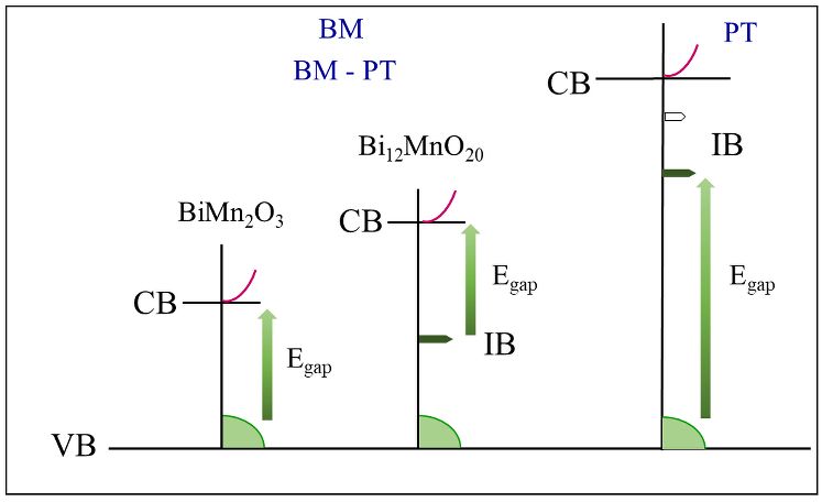
Figure 5. Secondary electron images obtained for the composite ceramics: BM (a), 0.98 BM–0.02 PT
                                  (b), 0.96 BM–0.04 PT (c), 0.92 BM–0.08 PT (d), 0.88 BM–0.12 PT (e), 0.84 BM–0.16 PT (f), and 0.76
 Electron. Mater. 2022, 3         BM–0.24 PT (g).                                                                               106

                                        Survey spectra obtained for the reference BM and PT ceramics are shown in Figure
                                  6. The BM sample showed the occurrence of manganate Mn, bismuth Bi, oxygen O, and
                                        Survey spectra obtained for the reference BM and PT ceramics are shown in Figure 6.
                                  gold Au. The occurrence of Au line relates to the gold-sputtered on the samples. The PT
                                  The BM sample showed the occurrence of manganate Mn, bismuth Bi, oxygen O, and gold
                                  showed the occurrence of lead Pb, titanate Ti, O, and Au. The EDS analysis was performed
                                  Au. The occurrence of Au line relates to the gold-sputtered on the samples. The PT showed
                                  for areas of 300 × 300 μm2 (see Table 1). For the metal elements, the nominal chemical
                                  the occurrence of lead Pb, titanate Ti, O, and Au. The EDS analysis was performed for areas
                                  composition ratio     is: Bi:Mn = 50.0:50.0 for BM ceramics, and Pb:Ti = 50.0: 50.0 for perov-
                                  of 300 × 300 µm2 (see Table 1). For the metal elements, the nominal chemical composition
                                  skite PT. The EDS analysis showed, for BM ceramics, a real composition close to the nom-
                                  ratio is: Bi:Mn = 50.0:50.0 for BM ceramics, and Pb:Ti = 50.0:50.0 for perovskite PT. The EDS
                                  inal one. In the case of PT we observed a higher amount of Ti. This effect could be related
                                  analysis showed, for BM ceramics, a real composition close to the nominal one. In the case
                                  to the evaporation of Pb during the sintering because of the high volatility of lead oxides.
                                  of PT we observed a higher amount of Ti. This effect could be related to the evaporation of
                                  For  BM-PTthe
                                  Pb during     ceramics,
                                                   sintering survey  spectra
                                                               because       are
                                                                        of the    shown
                                                                               high       in Figure
                                                                                      volatility      7. The
                                                                                                 of lead     samples
                                                                                                         oxides.       showed
                                                                                                                 For BM-PT      the oc-
                                                                                                                              ceramics,
                                  currence   of Mn,  Bi, Ti, Pb, and  Au. The  EDS  analysis   for Pb and Bi content is
                                  survey spectra are shown in Figure 7. The samples showed the occurrence of Mn, Bi, Ti,vague  because
                                  of
                                  Pb,similar
                                       and Au.energy   for these
                                                 The EDS          two elements.
                                                             analysis for Pb andHence,    quantitative
                                                                                   Bi content  is vague estimation
                                                                                                         because of suffers
                                                                                                                    similarfrom   over-
                                                                                                                             energy for
                                  lapping   of Pb and   Bi most  intensive lines in the analyzed    spectrum. However,
                                  these two elements. Hence, quantitative estimation suffers from overlapping of Pb and Bithe obtained
                                  element   contentlines
                                  most intensive      is close  to analyzed
                                                           in the  expected. spectrum.
                                                                             There are no    impurities
                                                                                         However,     the detected
                                                                                                          obtained in all studies
                                                                                                                   element        sam-
                                                                                                                             content is
                                  ples.
                                  close to expected. There are no impurities detected in all studies samples.

Electron. Mater. 2022, 3, FOR PEER REVIEW                                                                                                 7

                                  Figure 6.
                                  Figure    The survey
                                         6. The survey spectra
                                                       spectra obtained
                                                               obtained for:
                                                                        for: (a)
                                                                             (a) BM
                                                                                 BM and
                                                                                    and (b)
                                                                                        (b) PT
                                                                                            PT ceramics.
                                                                                               ceramics.

                                  Figure 7. The survey spectra obtained for: (a) 0.96 BM–0.04 PT, (b) 0.88 BM–0.12 PT, and (c) 0.76 BM–
                                  Figure 7. The survey spectra obtained for: (a) 0.96 BM–0.04 PT, (b) 0.88 BM–0.12 PT, and (c) 0.76
                                  0.24 PT ceramics.
                                  BM–0.24 PT ceramics.

                                  Table 1. Exemplar atomic concentration (at%) estimated for chosen ceramics surfaces.

                                                                0.96 BM                        0.88 BM                       0.76 BM
  Atom            BM        Atom            PT     Atom                          Atom                          Atom
                                                                –0.04 PT                       –0.12PT                       –0.24 PT
Electron. Mater. 2022, 3                                                                                                         107

                                   Table 1. Exemplar atomic concentration (at%) estimated for chosen ceramics surfaces.

 Atom       BM         Atom     PT      Atom     0.96 BM–0.04 PT         Atom        0.88 BM–0.12PT         Atom   0.76 BM–0.24 PT
   Bi       50.2           Pb   48.5      Bi            45.0               Bi              43.6              Bi           36.5
  Mn        49.8           Ti   51.5     Mn             51.4              Mn               45.1             Mn            38.3
                                         Pb             1.5                Pb               6.2              Pb           13.8
                                          Ti            2.1                Ti               5.1              Ti           11.4

                                   3.2. Vis-NIR Optical Features
                                         The room temperature diffuse reflectance R spectra were measured in the 400–1000 nm
                                   range of Vis-NIR spectrum. For the graphical estimation of the difference in energy states,
                                   Egap , magnitude, the Vis-NIR spectra recorded in the R mode were transformed to Kubelka-
                                   Munk equation:
                                                                       F(R) = (1 − R)2 /2R                                 (1)
                                   which is proportional to the extinction coefficient, α. Determination of Egap was conducted
                                   using the Tauc method and relation of incident photon energy, E = hν, with the modified
                                   Kubelka-Munk function:
                                                                     (α·hν)1/n ≈ B(hν − Egap )                              (2)
                                         We presumed the indirect allowed transitions in the BM-PT composite. Hence,
                                   (α·hν)1/n vs. hν plots, where exponent n = 2, were applied for analysis. The Egap was
                                   estimated by extrapolating the straight-line segment to the intersection with the hν axis,
                                   that is for (αhν)1/2 = 0 [51,52].
                                         We note that the PT, BiMn2 O5 , Bi12 MnO20 , and their derivative phases, which resulted
                                   from sintering, bring in individual electronic structure contributions. Moreover, the mutual
                                   migration ions and V O defects may introduce intermediate band gap states and tails in
                                   the vicinity of the VB and conductivity band, CB, [24,43]. Therefore, any superposition
                                   spectrum, obtained for a doping-modified and two-phase semiconductor, is the ‘effective’
                                   linear combination of the spectra of both components:

                                                                    (α(hν))eff = a·α1 (hν) + b·α2 (hν))                          (3)

                                   where a and b determine the components’ concentrations contributions, while α1 (hν) and
                                   α2 (hν) are the absorption coefficients of the assumed two phases contribution [6,44,52,53].
                                   Therefore, an effective energy gap is determined using the Tauc relation:

                                                                   {[(α(hν))eff ] hν)}1/2 = B(hν − Egap )                        (4)

                                        Following the proposed approximation, we decided to conduct the spectra analysis
                                   using the Tauc method [44,51]. We performed extrapolation where straight-line slopes
                                   could be distinguished.
                                        The diffuse reflectance spectra of BM and PT reference ceramics are shown in Figure 8.
                                   The R(λ) increased when wavelength increased, more steeply for λ > 900 nm. A broad
                                   hump occurred in ~550–800 nm range, corresponding to red and dark red light. The most
                                   distinct difference occurred in the 400–550 nm range, where PT reflectance exhibited a steep
                                   change in R magnitude, contrary to the BM sample.
                                        We discerned the straight-line segment in the Tauc plot obtained for the reference
                                   BM self-composite, and Egap (NIR) = 1.20 eV was estimated for the NIR spectrum range
                                   (Figure 9a). Egap (Vis) = 2.45 eV was estimated in the case of the reference PT compound
                                   (Figure 9b).
could
                           distinctbedifference
                                      distinguished.
                                                occurred in the 400–550 nm range, where PT reflectance exhibited a
                           steep change in R magnitude,spectra
                                The   diffuse reflectance         oftoBM
                                                           contrary    theand
                                                                           BMPT reference ceramics are shown in Figure
                                                                              sample.
                           8. The R(λ) increased when wavelength increased, more steeply for λ > 900 nm. A broad
                           hump occurred in ~550–800 nm range, corresponding to red and dark red light. The most
Electron. Mater. 2022, 3                                                                                     108
                           distinct difference occurred in the 400–550 nm range, where PT reflectance exhibited      a
                           steep change in R magnitude, contrary to the BM sample.

                           Figure 8. Reflectance, R, vs. wavelengths, λ, dependence measured for BM (a) and PT (b).

                                We discerned the straight-line segment in the Tauc plot obtained for the reference
                           BM self-composite, and Egap(NIR) = 1.20 eV was estimated for the NIR spectrum range
                           (Figure 9a). Egap(Vis) = 2.45 eV was estimated in the case of the reference PT compound
                           (Figure
                           Figure 8.9b).
                           Figure 8. Reflectance,R,R,vs.vs.wavelengths,
                                     Reflectance,           wavelengths,   λ, dependence
                                                                        λ, dependence    measured
                                                                                      measured      for(a)
                                                                                               for BM   BM   (a)PT
                                                                                                           and   and
                                                                                                                   (b).PT (b).

                                We discerned the straight-line segment in the Tauc plot obtained for the reference
                           BM self-composite, and Egap(NIR) = 1.20 eV was estimated for the NIR spectrum range
                           (Figure 9a). Egap(Vis) = 2.45 eV was estimated in the case of the reference PT compound
                           (Figure 9b).

                           Figure    Modified Kubelka-Munk
                           Figure 9. Modified Kubelka-Munkfunction  (αhν1/2
                                                           function(αhν) )1/2 vs.
                                                                              vs. photon energyhνhνplot
                                                                                  photonenergy      plotobtained
                                                                                                         obtainedforfor
                                                                                                                      BMBM
                                                                                                                         (a)(a)
                           and
                           and PT (b).

                                 R(λ) spectra obtained for (1 − x) BM–x PT composites are shown in Figure 10. R
                           magnitude decreased when the PT content increased, from ~50–80% to ~25–30% despite
                           that the reference PT R(λ) varied in the 40–100 % range (compare Figures 6 and 8). The R(λ)
                           common feature was its magnitude increase when wavelength increased and a more steep
                           Figure 9. Modified Kubelka-Munk function (αhν)1/2 vs. photon energy hν plot obtained for BM (a)
                           change in R magnitude for λ > 900 nm. A more or less distinct broad hump occurred in
                           and PT (b).
                           ~550–800 nm range; it shifted toward NIR range and became negligible for high content of
                           PT component.
                                 Graphical representation of the modified Kubelka–Munk function allowed us to
                           determine Egap magnitude dependence on the (1 − x) BM–x PT ceramics composition
                           (Figures 11 and 12). The Egap (NIR) of the order of ~1 eV was estimated for BM-PT ceramics,
                           and it showed a tendency to fluctuate with PT content change (Figure 12).
R(λ) spectra obtained for (1−x) BM–x PT composites are shown in Figure 10. R mag-
                                    nitude decreased when the PT content increased, from ~50–80% to ~25–30% despite that
                                    the reference PT R(λ) varied in the 40–100 % range (compare Figures 6 and 8). The R(λ)
                                    common feature was its magnitude increase when wavelength increased and a more steep
                                    change in R magnitude for λ > 900 nm. A more or less distinct broad hump occurred in
  Electron. Mater. 2022, 3                                                                                             109
                                    ~550–800 nm range; it shifted toward NIR range and became negligible for high content
                                    of PT component.

Electron. Mater. 2022, 3, FOR PEER REVIEW                                                                                                                10
                                    Figure 10. Reflectance, R, vs. wavelengths, λ      λ,, dependence              (1 − x)
                                                                                           dependence measured for (1−x) BM–x PTPT
                                                                                                                           BM–x  ceramics, x
                                                                                                                                   ceramics,
                                    = 0.02, 0.04, 0.08, 0.12, 0.16, 0.24, (a–f), respectively.
                                    x = 0.02, 0.04, 0.08, 0.12, 0.16, 0.24, (a–f), respectively.

                                         Graphical representation of the modified Kubelka–Munk function allowed us to de-
                                    termine Egap magnitude dependence on the (1−x) BM–x PT ceramics composition (Figures
                                    11 and 12). The Egap(NIR) of the order of ~1 eV was estimated for BM-PT ceramics, and it
                                    showed a tendency to fluctuate with PT content change (Figure 12).

                                    Figure11.
                                    Figure  11.Modified
                                                Modified   Kubelka-Munk
                                                        Kubelka-Munk             function
                                                                            function          1/2 νvs.
                                                                                       (αhν)(αh     )1/2photon
                                                                                                         vs. photon
                                                                                                                 energyenergy    ν plot obtained
                                                                                                                         hν plothobtained for (1 − x)
                                                                                                                                                   for (1−x)
                                    BM–xPT
                                    BM–x   PTceramics,
                                              ceramics,x x= =0.02,
                                                               0.02, 0.04,
                                                                   0.04,    0.08,
                                                                         0.08,    0.12,
                                                                               0.12, 0.16,0.16,
                                                                                            0.24,0.24,
                                                                                                   (a–f),(a–f), respectively.
                                                                                                           respectively.
Electron. Mater. 2022, 3                                                                                                                          110
                                     Figure 11. Modified Kubelka-Munk function (αhν)1/2 vs. photon energy hν plot obtained for (1−x)
                                     BM–x PT ceramics, x = 0.02, 0.04, 0.08, 0.12, 0.16, 0.24, (a–f), respectively.

                                     Figure 12.
                                     Figure                                                     (1 − x)
                                              12. Optical energy gaps estimated for BM, PT, and (1−x) BM–x PTPT
                                                                                                        BM–x  ceramic composites
                                                                                                                ceramic          (x =
                                                                                                                        composites
                                     0.02,
                                     (x    0.04,0.04,
                                        = 0.02,  0.08,0.08,
                                                       0.12,0.12,
                                                              0.16,0.16,
                                                                     andand
                                                                         0.24).
                                                                            0.24).

                                    4.
                                    4. Discussion
                                       Discussion
                                         The
                                          The reference
                                                referencefor forPT PTceramics
                                                                       ceramicswas   wasthetheone-phase
                                                                                                one-phasecompound.
                                                                                                              compound.The    Thelight-yellow
                                                                                                                                    light-yellow color
                                                                                                                                                   color
                                    of this material suggested that the actual Egap magnitude originated from a defected
                                    of this material suggested that the actual Egap magnitude originated from a defected PT
                                    PT structure would be lower from Egap = 3.4 eV reported for the ideal stoichiometric
                                    structure would be lower from Egap = 3.4 eV reported for the ideal stoichiometric transpar-
                                    transparent crystal [29,30]. We note that the Egap = 3.4 eV of such PT can only be detected
                                    ent crystal [29,30]. We note that the Egap = 3.4 eV of such PT can only be detected in the UV
                                    in the UV range, which was beyond our study frames. Hence, the Egap (Vis) = 2.45 eV
                                    range, which was beyond our study frames. Hence, the Egap(Vis) = 2.45 eV (Figure 9b)
                                    (Figure 9b) should correspond to the effects of defects and disorder. One notes that V O
                                    should correspond to the effects of defects and disorder. One notes that VO defects intro-
                                    defects introduce shallow and deep energy levels in the perovskite ABO3 structures [24].
                                    duce   shallow and
                                    Such deduction          deep
                                                         also       energyby
                                                               is justified    levels  in the perovskite
                                                                                  the literature    reports. ABO     3 structures [24]. Such deduc-
                                                                                                              It is consistent    with the results of
                                    tion also  is justified   by   the  literature   reports.   It is consistent
                                    calculations provided for defected PT, reported in the literature, where        with   the results  of calculations
                                                                                                                                   the full potential
                                    linearized augmented plane-wave calculation exhibited that oxygen vacancieslinearized
                                    provided     for  defected      PT,   reported    in  the  literature,   where     the  full potential     induce
Electron. Mater. 2022, 3, FOR PEER REVIEW
                                    augmentedin-gapplane-wave        calculation     exhibited    that  oxygen    vacancies     induce additional    11
                                    additional              Ti 3d states     -1.1 eV   below the      Fermi   energy    [54]. Indirect   optical gapin-
                                    gap Ti from
                                    varied   3d states
                                                    2.78-1.1
                                                           eV eV    below
                                                                to 3.66    eVthe   Fermi energy
                                                                               dependably            [54].PT
                                                                                                on the     Indirect
                                                                                                              surfaceoptical    gap varied
                                                                                                                         termination          from
                                                                                                                                        [31,55].    2.78
                                                                                                                                                  The
                                    eV  to  3.66  eV   dependably        on  the   PT  surface    termination     [31,55].
                                    experimentally determined Egap = 2.6 eV seems to be also related to the defects subsystemThe  experimentally     de-
                                    termined
                                    Therefore,
                                    of           E      =
                                       PT [56]. ETherefore,2.6  eV
                                                    gap(Vis) = 2.45
                                                   gap               seems
                                                                   EgapeV       to
                                                                            should
                                                                         (Vis)      be
                                                                                = 2.45  also
                                                                                      be eV    related
                                                                                         attributed
                                                                                              should to  to
                                                                                                        bethethe   defects
                                                                                                               gap between
                                                                                                            attributed        subsystem
                                                                                                                          to thethe
                                                                                                                                  gap       of  PT
                                                                                                                                      defect-induced
                                                                                                                                        between the [56].
                                    sub-band and CB,
                                    defect-induced           which and
                                                        sub-band       position     and possible
                                                                             CB, which      positiontails
                                                                                                       andwere     determined
                                                                                                            possible    tails were bydetermined
                                                                                                                                       crystal lattice
                                                                                                                                                    by
                                    crystal
                                    disorder.lattice
                                                These disorder.
                                                         literatureThese
                                                                      Egapliterature    Egap data
                                                                             data are shown           are shown
                                                                                                 in Figure    13. in Figure 13.

                                     Figure 13. The diagram compares E
                                     Figure 13.                                 Egap magnitudes, available
                                                                                 gap magnitudes, available from
                                                                                                           from cited literature reports for
                                                                                                                                         for
                                     BiMn22O55,, Bi
                                     BiMn        Bi1212MnO
                                                       MnO20,20,and
                                                                 andPbTiO
                                                                     PbTiO
                                                                         3. 3 .

                                        The BM and BM-PT ceramics are multi-phase composites [37,48,49]. BM is the self-
                                     composite consisting of the major BiMn2O5 and the minor Bi12MnO20 phase. The BM-PT
                                     composite consists of phases, which structure changed because of mutual migration of
Electron. Mater. 2022, 3                                                                                            111

                                 The BM and BM-PT ceramics are multi-phase composites [37,48,49]. BM is the self-
                           composite consisting of the major BiMn2 O5 and the minor Bi12 MnO20 phase. The BM-PT
                           composite consists of phases, which structure changed because of mutual migration of
                           ions when the ceramics were sintered from the reference BM and PT [46,50]. For instance,
                           it would be noted that the Bi2 O3 phase, iso-structural with Bi20 TiO32 , transformed from
                           the Bi12 MnO20 parent phase of the BM self-composite [50]. Moreover, local fluctuations in
                           composition and the occurrence of oxygen deficiency cannot be excluded. The graphite-
                           black color of these BM-PT compounds indicated marked light absorbance in the Vis range.
                                 Therefore, the measured R(λ) spectra were considered as effective quantities, which
                           included contributions from individual phases of the BM-PT system. It should be noted
                           that the lower R magnitude occurred when the PT content in the BM-PT ceramics was
                           higher. The R magnitude decrease from ~50–80% to ~25–30% indicated an active role of the
                           PT component and influence porosity. Similar to a glassy black mirror, a standard flat and
                           smooth surface usually offers reflectance on a 40–50% level. Lower R would be achieved in
                           the case of a textured surface when light is scattered and absorbed more effectively [57]. It
                           should be noticed that the SEM test exhibited porosity and concave voids in the BM-PT
                           ceramics surfaces.
                                 We note that the reference PT powder grain was much smaller than the BM-PT com-
                           pounds grain (compare Figure 1b to Figures 1a, 2, 3, 4 and 5). Hence, we deduce that
                           tiny grains of the PT powder introduced to the sintered BM-PT ceramics also would be
                           responsible for this effect. We conclude that both the small grains of the PT component and
                           the porous texture of BM-PT ceramics surface may facilitate scattering, decrease R to ~25%,
                           and enhance light absorption. We noticed a correlation between R and ceramics morphol-
                           ogy. The BM, 0.96 BM–0.04 PT, and PT ceramics showed R higher magnitude and more
                           homogenous morphology than the other doped BM-PT ceramics. Moreover, the BM and
                           PT samples were characterized by the smaller grains and the highest reflectance. Therefore,
                           despite any uncontrolled and random factors that cannot be excluded a priori, we deduce
                           that the low reflectance of the BM-PT ceramics can relate to the rough surface features.
                                 We applied the Tauc procedure within the NIR following the assumed effective re-
                           flectance spectrum superposition obtained for the BM and BM-PT multi-phase compos-
                           ites [43,44,58]. The Egap (NIR) = 1.20 eV, estimated for the BM self-composite, correlates
                           to the literature data. The studied herein BM consists of the major BiMn2 O5 phase and
                           minor Bi12 MnO20 phase. One notices that the Egap = 1.24 eV was reported BiMn2 O5
                           compound [44]. The case of Bi12 MnO20 compound offers more possible charge trans-
                           fers determined by Wu et al. [43]: the charge excitation between VB and CB of intrinsic
                           Egap = 1.86 eV, other from the VB to the intermediate band, IB, of ~0.79 eV, and also ex-
                           citation from the intermediate band to the CB of ~1.07 eV (see Figure 13). Therefore, we
                           do not assign the effective Egap (NIR) = 1.20 eV to specific phase. Such the choice would
                           be vague due to the similarity of the energy gap size; either Egap = 1.24 eV of BiMn2 O5 ,
                           or Egap = 1.07 eV of Bi12 MnO20 can be chosen. We note that the coincidence of estimated
                           herein Egap (NIR) = 1.20 eV to the literature reports on the perovskite BiMnO3 compound
                           (Egap = 1.1 eV) is random due to this unstable perovskite phase was not detected in case
                           of the studied herein BM. In the case of the (1 − x) BM–x PT compounds, the obtained
                           magnitude of Egap fluctuated on Egap (NIR) = 1.00 ± 0.15 eV level (see Figure 12). We
                           deduce an effective role of local disorder, which would influence the electronic structure of
                           the studied material. The V O occurrence would induce an additional sub-bands within the
                           energy gap [24]. In case of the Bi12 MnO20 phase, the V O creates the IB band, mentioned
                           above, which can be responsible for the charge transfer. However, in case of the BiMn2 O5 ,
                           additional IB energy levels, leading to lower than 1 eV excitation energy, were not observed,
                           using the applied NIR range. We propose that defects, most probably caused by mutual
                           diffusion of ions between the phases, resulting from the final sintering procedure [46,50],
                           create tails of states in the VB and CB that lead to the detected narrowing of the energy gap
                           (see diagram in Figure 14).
rence would induce an additional sub-bands within the energy gap [24]. In case of the
                                    Bi12MnO20 phase, the VO creates the IB band, mentioned above, which can be responsible
                                    for the charge transfer. However, in case of the BiMn2O5, additional IB energy levels, lead-
                                    ing to lower than 1.eV excitation energy, were not observed, using the applied NIR range.
                                    We propose that defects, most probably caused by mutual diffusion of ions between the
Electron. Mater. 2022, 3                                                                                                        112
                                    phases, resulting from the final sintering procedure [46,50], create tails of states in the VB
                                    and CB that lead to the detected narrowing of the energy gap (see diagram in Figure 14).

                                    Figure 14.
                                    Figure 14. A schematic band,
                                                           band, E
                                                                 Egap
                                                                   gap,,layout
                                                                         layout proposed
                                                                                proposed for
                                                                                         for BM,
                                                                                             BM, BM-PT,
                                                                                                 BM-PT, and PT ceramics, obtained from
                                                                                                                                  from
                                    performed  Vis-NIR test.
                                    performed Vis-NIR test.

                                       In summary,
                                          summary, wewe would
                                                        would emphasize
                                                              emphasize the
                                                                        the most
                                                                            most important
                                                                                  important properties
                                                                                            properties of
                                                                                                       of studied
                                                                                                          studied herein
                                                                                                                  herein
                                    composite ceramics.
                                    composite ceramics.
                                    1.
                                    1.    In the case of BM and PT reference materials, it was possible to attribute determined   determined
                                          Egap
                                            gapmagnitudes
                                                magnitudesto toelectric
                                                                 electric charge
                                                                          charge excitation
                                                                                    excitation from the VB to CB (BiMn  (BiMn22O55),), to
                                                                                                                                       to transi-
                                          tion from IB to the CB (Bi12    MnO2020),),and
                                                                       12MnO          andfrom
                                                                                          fromVB  VBtotoIB
                                                                                                         IB(PT);
                                                                                                             (PT);
                                    2.
                                    2.    The (1  − x)BM–x
                                               (1−x)   BM–xPT PTcomposite      exhibited Egap
                                                                  composite exhibited                       1.00 ±
                                                                                                  (NIR) == 1.00
                                                                                              gap(NIR)           ± 0.15
                                                                                                                    0.15 eV lower      thanEEgap
                                                                                                                              lower than       gap

                                          magnitudes of thethe reference
                                                               referencecompounds.
                                                                            compounds.This  Thisgapgapnarrowing
                                                                                                        narrowingeffect
                                                                                                                      effectoriginated
                                                                                                                             originated   from
                                                                                                                                            froma
                                          disorder;
                                          a disorder;
                                    3.
                                    3.    Determined properties
                                          Determined                      (1 −BM–x
                                                        propertiesofof(1−x)     x) BM–x      PT, especially
                                                                                        PT, especially         the narrowing
                                                                                                         the narrowing     of the of
                                                                                                                                  Egapthe   Egap
                                                                                                                                         magni-
                                          magnitudes,
                                          tudes,        of the of
                                                 of the order   order  of which
                                                                   1 eV,  1 eV, which    corresponds
                                                                                  corresponds            to marked
                                                                                                   to marked    light light absorption
                                                                                                                       absorption    in Visinand
                                                                                                                                              Vis
                                          and NIR,
                                          NIR,       suggest
                                                suggest       potential
                                                         potential        optoelectrical
                                                                     optoelectrical         applications.
                                                                                       applications.

                                    Author Contributions:
                                    Author    Contributions: Conceptualization,
                                                             Conceptualization, A.M.;
                                                                                  A.M.; methodology,
                                                                                        methodology, A.M.,
                                                                                                       A.M., A.Z.S.,
                                                                                                              A.Z.S., J.K.;
                                                                                                                      J.K.; validation,
                                                                                                                            validation, A.M.,
                                                                                                                                        A.M.,
                                    A.Z.S.  J.K.; formal analysis, A.M., A.Z.S.; investigation, A.M., A.Z.S., J.K.; writing—original    draft
                                    A.Z.S., J.K.; formal analysis, A.M., A.Z.S.; investigation, A.M., A.Z.S., J.K.; writing—original draft
                                    preparation, A.M.; writing—review and editing, A.M., A.Z.S.; visualization, A.M., A.Z.S.; funding
                                    acquisition, A.M., A.Z.S. All authors have read and agreed to the published version of the manuscript.
                                    Funding: A.M. and A.Z.S. note that this publication is co-financed by the funds granted under the
                                    Research Excellence Initiative of the University of Silesia in Katowice.
                                    Institutional Review Board Statement: Not applicable.
                                    Data Availability Statement: Not applicable.
                                    Conflicts of Interest: The authors declare no conflict of interest.

References
1.    Li, S.; Morasch, J.; Klein, A.; Chirila, C.; Pintilie, L.; Jia, L.; Ellmer, K.; Naderer, M.; Reichmann, K.; Gröting, M.; et al. Influence of
      orbital contributions to the valence band alignment of Bi2 O3 , Fe2 O3 , BiFeO3 , and Bi0.5 Na0.5 TiO3 . Phys. Rev. B 2013, 88, 045428.
      [CrossRef]
2.    Rühle, S. Tabulated values of the Shockley—Queisser limit for single junction solar cells. Sol. Energy 2016, 130, 139–147. [CrossRef]
3.    Ehrler, B.; Alarcón-Lladó, E.; Tabernig, S.W.; Veeken, T.; Garnett, E.C.; Polman, A. Photovoltaics Reaching for the Shockley–
      Queisser Limit. ACS Energy Lett. 2020, 5, 3029–3033. [CrossRef]
4.    Genenko, Y.A.; Glaum, J.; Hoffmann, M.J.; Albe, K. Mechanisms of aging and fatigue in ferroelectrics. Mater. Sci. Eng. B 2015,
      192, 52–82. [CrossRef]
5.    Grinberg, I.; West, D.V.; Torres, M.; Gou, G.; Stein, D.M.; Wu, L.; Chen, G.; Gallo, E.M.; Akbashev, A.R.; Davies, P.K.; et al.
      Perovskite oxides for visible-light-absorbing ferroelectric and photovoltaic materials. Nature 2013, 503, 509–512. [CrossRef]
6.    Sheikh, M.S.; Ghosh, D.; Bhowmik, T.K.; Dutta, A.; Bhattacharyya, S.; Sinha, T.P. When multiferroics become photoelectrochemical
      catalysts: A case study with BiFeO3 /La2 NiMnO6 . Mater. Chem. Phys. 2020, 244, 122685. [CrossRef]
7.    Li, P.; Abe, H.; Ye, J. Band-Gap Engineering of NaNbO3 for Photocatalytic H2 Evolution with Visible Light. Int. J. Photoenergy
      2014, 2014, 380421. [CrossRef]
8.    Hwang, D.W.; Kim, H.G.; Lee, J.S.; Kim, J.; Li, W.; Oh, S.H. Photocatalytic Hydrogen Production from Water over M-Doped
      La2 Ti2 O7 (M = Cr, Fe) under Visible Light Irradiation (λ > 420 nm). J. Phys. Chem. B 2005, 109, 2093–2102. [CrossRef]
Electron. Mater. 2022, 3                                                                                                                  113

9.    Ma, C.; Liu, Z.; Cai, Q.; Han, C.; Tong, Z. ZnO photoelectrode simultaneously modified with Cu2 O and Co-Pi based on broader
      light absorption and efficiently photogenerated carrier separation. Inorg. Chem. Front. 2018, 5, 2571–2578. [CrossRef]
10.   Madusanka, H.T.D.S.; Herath, H.M.A.M.; Fernando, C.A.N. High photoresponse performance of self-powered n-Cu2 O/p-CuI
      heterojunction based UV-Visible photodetector. Sens. Actuators A Phys. 2019, 296, 61–69. [CrossRef]
11.   He, L.; Fei, M.; Chen, J.; Tian, Y.; Jiang, Y.; Huang, Y.; Xu, K.; Hu, J.; Zhao, Z.; Zhang, Q.; et al. Graphitic C3 N4 quantum dots for
      next-generation QLED displays. Mater. Today 2019, 22, 76–84. [CrossRef]
12.   Wang, D.; Ye, J.; Kako, T.; Kimura, T. Photophysical and Photocatalytic Properties of SrTiO3 Doped with Cr Cations on Different
      Sites. J. Phys. Chem. B 2006, 110, 15824–15830. [CrossRef] [PubMed]
13.   Bujakiewicz-Koronska, R.; Nalecz, D.M.; Molak, A.; Budziak, A. DOS calculation for stoichiometric and oxygen defected
      (Bi1/2 Na1/2 )(Mn1/2 Nb1/2 )O3 . Ferroelectrics 2014, 463, 48–56. [CrossRef]
14.   Shi, H.; Li, X.; Iwai, H.; Zou, Z.; Ye, J. 2-Propanol photodegradation over nitrogen-doped NaNbO3 powders under visible-light
      irradiation. J. Phys. Chem. Solids 2009, 70, 931–935. [CrossRef]
15.   Zheng, D.; Deng, H.; Pan, Y.; Guo, Y.; Zhao, F.; Yang, P.; Chu, J. Modified multiferroic properties in narrow bandgap (1 −
      x)BaTiO3 -xBaNb1/3 Cr2/3 O3-δ ceramics. Ceram. Int. 2020, 46, 26823–26828. [CrossRef]
16.   Varignon, J.; Bibes, M.; Zunger, A. Origin of band gaps in 3d perovskite oxides. Nat. Commun. 2019, 10, 1658. [CrossRef]
17.   Chen, L.; Zheng, G.; Yao, G.; Zhang, P.; Dai, S.; Jiang, Y.; Li, H.; Yu, B.; Ni, H.; Wei, S. Lead-Free Perovskite Narrow-Bandgap
      Oxide Semiconductors of Rare-Earth Manganates. ACS Omega 2020, 5, 8766–8776. [CrossRef]
18.   Butson, J.D.; Narangari, P.R.; Lysevych, M.; Wong-Leung, J.; Wan, Y.; Karuturi, S.K.; Tan, H.H.; Jagadish, C. InGaAsP as
      a Promising Narrow Band Gap Semiconductor for Photoelectrochemical Water Splitting. ACS Appl. Mater. Interfaces 2019,
      11, 25236–25242. [CrossRef]
19.   Sathe, A.; Seki, M.; Zhou, H.; Chen, J.X.; Tabata, H. Bandgap engineering in V-substituted α-Fe2 O3 photoelectrodes. Appl. Phys.
      Express 2019, 12, 091003. [CrossRef]
20.   Gadhoumi, F.; Kallel, I.; Benzarti, Z.; Abdelmoula, N.; Hamedoun, M.; Elmoussaoui, H.; Mezzane, D.; Khemakhem, H.
      Investigation of magnetic, dielectric and optical properties of BiFe0.5 Mn0.5 O3 multiferroic ceramic. Chem. Phys. Lett. 2020,
      753, 137569. [CrossRef]
21.   Molak, A.; Pilch, M. Visible light absorbance enhanced by nitrogen embedded in the surface layer of Mn-doped sodium niobate
      crystals, detected by ultra violet—visible spectroscopy, x-Ray photoelectron spectroscopy, and electric conductivity tests. J. Appl.
      Phys. 2016, 119, 204901. [CrossRef]
22.   Mefford, J.T.; Hardin, W.G.; Dai, S.; Johnston, K.P.; Stevenson, K.J. Anion charge storage through oxygen intercalation in LaMnO3
      perovskite pseudocapacitor electrodes. Nat. Mater. 2014, 13, 726–732. [CrossRef] [PubMed]
23.   Huang, Y.; Wei, Y.; Cheng, S.; Fan, L.; Li, Y.; Lin, J.; Wu, J. Photocatalytic property of nitrogen-doped layered perovskite
      K2 La2 Ti3 O10 . Sol. Energy Mater. Sol. Cells 2010, 94, 761–766. [CrossRef]
24.   Prosandeyev, S.A.; Teslenko, N.M.; Fisenko, A. V Breaking of symmetry of one-electron orbitals at oxygen vacancies in perovskite-
      type oxides. J. Phys. Condens. Matter 1993, 5, 9327–9344. [CrossRef]
25.   Srivastava, S. Study of Band Gap Tunablity in one-dimensional Photonic Crystals of Multiferroic-dielectric materials: Case Study
      in Near Infrared Region. SOP Trans. Appl. Phys. 2014, 2014, 22–32. [CrossRef]
26.   Benjwal, P.; Kar, K.K. Removal of methylene blue from wastewater under a low power irradiation source by Zn, Mn co-doped
      TiO2 photocatalysts. RSC Adv. 2015, 5, 98166–98176. [CrossRef]
27.   Xu, X.S.; Ihlefeld, J.F.; Lee, J.H.; Ezekoye, O.K.; Vlahos, E.; Ramesh, R.; Gopalan, V.; Pan, X.Q.; Schlom, D.G.; Musfeldt, J.L. Tunable
      band gap in Bi(Fe1−x Mnx )O3 films. Appl. Phys. Lett. 2010, 96, 192901. [CrossRef]
28.   Mocherla, P.S.V.; Karthik, C.; Ubic, R.; Ramachandra Rao, M.S.; Sudakar, C. Tunable bandgap in BiFeO3 nanoparticles: The role of
      microstrain and oxygen defects. Appl. Phys. Lett. 2013, 103, 022910. [CrossRef]
29.   Niu, P.J.; Yan, J.L.; Xu, C.Y. First-principles study of nitrogen doping and oxygen vacancy in cubic PbTiO3 . Comput. Mater. Sci.
      2015, 98, 10–14. [CrossRef]
30.   Zametin, V.I. Absorption Edge Anomalies in Polar Semiconductors and Dielectrics at Phase Transitions. Phys. Status Solidi 1984,
      124, 625–640. [CrossRef]
31.   Piskunov, S.; Kotomin, E.A.; Heifets, E.; Maier, J.; Eglitis, R.I.; Borstel, G. Hybrid DFT calculations of the atomic and electronic
      structure for ABO3 perovskite (001) surfaces. Surf. Sci. 2005, 575, 75–88. [CrossRef]
32.   Molak, A.; Wöjcik, K. Optic properties and EPR spectra of PbTiO3 :Mn crystals. Ferroelectrics 1992, 125, 349–354. [CrossRef]
33.   Leonarska, A.; Ujma, Z.; Molak, A. Nano-size grain powders and ceramics of PbTiO3 obtained by the hydrothermal method and
      their electrical properties. Ferroelectrics 2014, 466, 42–50. [CrossRef]
34.   Belik, A.A. Polar and nonpolar phases of BiMO3 : A review. J. Solid State Chem. 2012, 195, 32–40. [CrossRef]
35.   Samuel, V.; Navale, S.C.; Jadhav, A.D.; Gaikwad, A.B.; Ravi, V. Synthesis of ultrafine BiMnO3 particles at 100 ◦ C. Mater. Lett. 2007,
      61, 1050–1051. [CrossRef]
36.   Molak, A.; Mahato, D.K.; Szeremeta, A.Z. Synthesis and characterization of electrical features of bismuth manganite and bismuth
      ferrite: Effects of doping in cationic and anionic sublattice: Materials for applications. Prog. Cryst. Growth Charact. Mater. 2018,
      64, 1–22. [CrossRef]
37.   Pilch, M.; Molak, A.; Koperski, J.; Zajdel, P. Influence of nitrogen flow during sintering of bismuth manganite ceramics on grain
      morphology and surface disorder. Phase Transit. 2017, 90, 112–124. [CrossRef]
Electron. Mater. 2022, 3                                                                                                                  114

38.   Muñoz, A.; Alonso, J.A.; Casais, M.T.; Martínez-Lope, M.J.; Martínez, J.L.; Fernández-Díaz, M.T. Magnetic structure and properties
      of BiMn2 O5 . Phys. Rev. B 2002, 65, 144423. [CrossRef]
39.   Chakrabartty, J. Oxide Perovskites for Solar Energy Conversion. Ph.D. Thesis, University of Quebec, Quebec, QC, Canada, 2018.
40.   Gaikwad, V.M.; Goyal, S.; Yanda, P.; Sundaresan, A.; Chakraverty, S.; Ganguli, A.K. Influence of Fe substitution on structural and
      magnetic features of BiMn2 O5 nanostructures. J. Magn. Magn. Mater. 2018, 452, 120–128. [CrossRef]
41.   Zhang, J.; Xu, B.; Li, X.F.; Yao, K.L.; Liu, Z.L. Origin of the multiferroicity in BiMn2 O5 from first-principles calculations. J. Magn.
      Magn. Mater. 2011, 323, 1599–1605. [CrossRef]
42.   Li, N.; Yao, K.; Gao, G.; Sun, Z.; Li, L. Charge, orbital and spin ordering in multiferroic BiMn2 O5 : Density functional theory
      calculations. Phys. Chem. Chem. Phys. 2011, 13, 9418. [CrossRef] [PubMed]
43.   Wu, X.; Li, M.; Li, J.; Zhang, G.; Yin, S. A sillenite-type Bi12 MnO20 photocatalyst: UV, visible and infrared lights responsive
      photocatalytic properties induced by the hybridization of Mn 3d and O 2p orbitals. Appl. Catal. B Environ. 2017, 219, 132–141.
      [CrossRef]
44.   Chakrabartty, J.P.; Nechache, R.; Harnagea, C.; Rosei, F. Photovoltaic effect in multiphase Bi-Mn-O thin films. Opt. Express 2014,
      22, A80. [CrossRef] [PubMed]
45.   Szeremeta, A.Z.; Pawlus, S.; Nowok, A.; Grzybowska, K.; Zubko, M.; Molak, A. Hydrostatic pressure influence on electric
      relaxation response of bismuth manganite ceramics. J. Am. Ceram. Soc. 2020, 103, 3732–3738. [CrossRef]
46.   Szeremeta, A.Z.; Nowok, A.; Zubko, M.; Pawlus, S.; Gruszka, I.; Koperski, J.; Molak, A. Influence of interfacial stresses on
      electrical properties of bismuth manganite—lead titanate—epoxy composite. Ceram. Int. 2021, 47, 34619–34632. [CrossRef]
47.   Szeremeta, A.Z. Relaxation Processes in Bismuth Manganite Which Was a Matrix for PbTiO3 or Was Doped to Pb(Zr0.70 Ti0.30 )O3
      Ceramics. Ph.D. Thesis, University of Silesia, Katowice, Poland, 2018. (In Polish).
48.   Molak, A.; Leonarska, A.; Szeremeta, A. Electric current relaxation and resistance switching in non-homogeneous bismuth
      manganite. Ferroelectrics 2015, 485, 161–172. [CrossRef]
49.   Molak, A.; Ujma, Z.; Pilch, M.; Gruszka, I.; Pawelczyk, M. Resistance switching induced in BiMnO3 ceramics. Ferroelectrics 2014,
      464, 59–71. [CrossRef]
50.   Molak, A.; Szeremeta, A.Z.; Zubko, M.; Nowok, A.; Balin, K.; Gruszka, I.; Pawlus, S. Influence of hydrostatic pressure on electrical
      relaxation in non-homogeneous bismuth manganite—Lead titanate ceramics. J. Alloys Compd. 2021, 854, 157219. [CrossRef]
51.   López, R.; Gómez, R. Band-gap energy estimation from diffuse reflectance measurements on sol–gel and commercial TiO2 :
      A comparative study. J. Sol-Gel Sci. Technol. 2012, 61, 1–7. [CrossRef]
52.   Zanatta, A.R. Revisiting the optical bandgap of semiconductors and the proposal of a unified methodology to its determination.
      Sci. Rep. 2019, 9, 11225. [CrossRef]
53.   Makuła, P.; Pacia, M.; Macyk, W. How to Correctly Determine the Band Gap Energy of Modified Semiconductor Photocatalysts
      Based on UV–Vis Spectra. J. Phys. Chem. Lett. 2018, 9, 6814–6817. [CrossRef]
54.   Cai, M.-Q.; Tang, C.-H.; Tan, X.; Deng, H.-Q.; Hu, W.-Y.; Wang, L.-L.; Wang, Y.-G. First-principles study for the atomic structures
      and electronic properties of PbTiO3 oxygen-vacancies (001) surface. Surf. Sci. 2007, 601, 5412–5418. [CrossRef]
55.   de Lazaro, S.; Longo, E.; Sambrano, J.R.; Beltrán, A. Structural and electronic properties of PbTiO3 slabs: A DFT periodic study.
      Surf. Sci. 2004, 552, 149–159. [CrossRef]
56.   Gerges, M.K.; Mostafa, M.; Rashwan, G.M. Structural, optical and electrical properties of PbTiO3 nanoparticles prepared by
      Sol-Gel method. Int. J. Latest Res. Eng. Technol. 2016, 2, 42–49.
57.   Zhong, J.; Wu, W.; Liao, J.; Feng, W.; Jiang, Y.; Wang, L.; Kuang, D. The Rise of Textured Perovskite Morphology: Revolutionizing
      the Pathway toward High-Performance Optoelectronic Devices. Adv. Energy Mater. 2020, 10, 1902256. [CrossRef]
58.   Shamitha, C.; Senthil, T.; Wu, L.; Kumar, B.S.; Anandhan, S. Sol–gel electrospun mesoporous ZnMn2 O4 nanofibers with superior
      specific surface area. J. Mater. Sci. Mater. Electron. 2017, 28, 15846–15860. [CrossRef]
You can also read