TRABAJO FIN DE GRADO - Universidad Autónoma de ...
←
→
Page content transcription
If your browser does not render page correctly, please read the page content below
UNIVERSIDAD AUTÓNOMA DE MADRID
         ESCUELA POLITÉCNICA SUPERIOR

  Grado en Ingeniería de Tecnologías y Servicios de
                Telecomunicación

     TRABAJO FIN DE GRADO
  ANTENA COMPACTA DE DOBLE LAZO PARA
OPERACIÓN MULTIBANDA EN DISPOSITIVOS CON
               SENSORES

           Autora: Esther Álvarez Pardo
            Tutor: Jordi Romeu Robert
          Ponente: José Luis Masa Campos

                     Julio 2017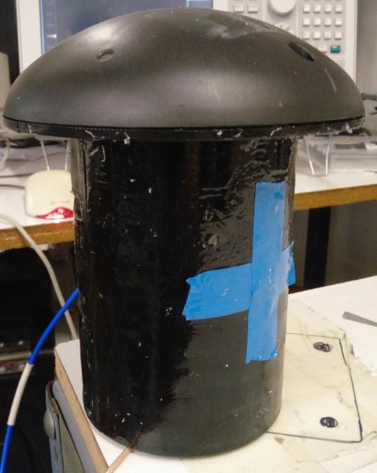
COMPACT DUAL-LOOP ANTENNA FOR MULTIBAND
      OPERATION IN SENSOR DEVICES

                    AUTHOR: Esther Álvarez Pardo
                    ADVISOR: Jordi Romeu Robert (*)
               CO-ADVISOR: José Luis Masa Campos (**)

(*) Escuela Técnica Superior de Ingeniería de Telecomunicación de Barcelona
                   Universitat Politècnica de Catalunya

                     (**) Escuela Politécnica Superior
                    Universidad Autónoma de Madrid
                                Julio 2017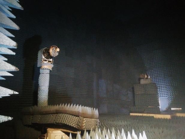
Dedicated to Fernando, Mari Luz and Mario.
Thank you for the endless support.
Title of the thesis: Compact dual-loop antenna for multiband operation in sensor
devices.

Author: Esther Álvarez Pardo.
Advisor: Jordi Romeu Robert.
Co-advisor: José Luis Masa Campos.

Abstract
       The aim of this Bachelor Thesis is to design, simulate and optimize a compact
dual-loop antenna in order to have resonant frequencies in the bands 800-1000 MHz and
1700-1900 MHz, suitable to be integrated within sensors.

Due to the rising number of smart interconnected devices that operate at different
frequency bands, constituting what is known as the Internet of Things, it is necessary to
provide with an antenna that not only enables communication - regardless the location -in
an efficient way, but also that is cost-effective, easy to produce and durable.

For this purpose, a first design was implemented, following the article [1] “Folded Dual-
Loop Antenna for GSM/DCS/PCS/UMTS Mobile Handset Applications”. To analyse its
behaviour throughout the simulations, the software tool CST Microwave Studio
(Computer Simulation Technology) was employed.

During this project, several optimizations were realized along with the design process so
as to have the antenna working for the two main frequency bands employed by the
wireless systems: Global System for Mobile Communications (GSM: 890–960 MHz) and,
Digital Cellular System (DCS: 1710–1880 MHz); taking into account as well the casing
effects of the sensor device.

Once the performance of the proposed design complied with the requirements with 10 dB
return loss, the antenna was fabricated. In order to validate the previous simulation results’
accuracy, the antenna was measured with and without its resin casing, physically
representing the same design that was developed at CST Microwave Studio.

Finally, the presented design proved to achieve good results and fractional bandwidth at a
lower cost when compared to existing solutions for internal antennas within sensor
devices.

                                                                                            1
Título del Trabajo de Fin de Grado: Compact dual-loop antenna for multiband
operation in sensor devices.

Autora: Esther Álvarez Pardo.
Tutor: Jordi Romeu Robert.
Ponente: José Luis Masa Campos.

Resumen
       El objetivo de este Trabajo de Fin de Grado es diseñar, simular, y optimizar una
antena compacta de doble lazo para obtener frecuencias de resonancia en las bandas 800-
1000 MHz y 1700-1900 MHz, apta para ser integrada con sensores.

Debido al creciente número de dispositivos inteligentes interconectados que operan en
diferentes bandas de frecuencia, constituyendo lo que se conoce como el Internet de las
Cosas, es necesario producir una antena que no sólo habilite la comunicación -
independientemente de la localización - de una manera eficiente, sino que también sea
rentable, fácil de producir y duradera.

Para este propósito, se implementó un primer diseño, siguiendo el artículo [1] “Folded
Dual-Loop Antenna for GSM/DCS/PCS/UMTS Mobile Handset Applications”. Para
analizar su comportamiento a través de las simulaciones, se utilizó la herramienta de
software CST Microwave Studio (Tecnología de Simulación Computacional).

Durante este proyecto, varias optimizaciones se llevaron a cabo junto con el proceso de
diseño para tener una antena funcionando en las dos bandas principales de frecuencia
utilizadas por los sistemas inalámbricos: Sistema Global de Comunicaciones Móviles
(GSM: 890–960 MHz) y, Sistema Celular Digital (DCS: 1710–1880 MHz); teniendo
también en cuenta los efectos de la carcasa del sensor.

Una vez que el comportamiento del diseño propuesto cumplía con los requisitos para
pérdidas de retorno a 10 dB, la antena fue fabricada. Para validar la exactitud de los
resultados de simulación previos, la antena se midió no sólo con su carcasa de resina sino
también sin ella, representando físicamente el mismo diseño desarrollado en CST
Microwave Studio.

Finalmente, el diseño presentado demostró conseguir buenos resultados y ancho de banda
fraccional a un coste más bajo al compararse con soluciones existentes para antenas
internas en dispositivos con sensores.

                                                                                        2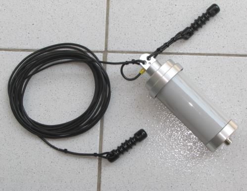
Acknowledgements
       I would like to express my gratitude to Prof. Jordi Romeu for giving me the
opportunity to develop this project. There are no words to describe how privileged I feel
for having your support and guidance throughout this year.

Thanks to Prof. José Luis Masa Campos and Marc Imbert for their advice and feedback,
and the laboratory technicians Ruben Tardio and Albert Marton for their support and
fabrication of the antenna.

I would also like to thank my lifetime friend Judit for believing in me during all these
years, encouraging me to keep moving forward.

Special thanks to my parents Mari Luz and Fernando, and my brother Mario for being an
inspiration and standing by my side in the tough times of my career and life. I wouldn´t be
who I am now without you.

And last but not least, I would like to thank that one person who did not give up on me
and was always there.

                                                                                         3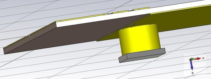
Keywords
Internet of things, IoT, dual-loop, compact, antenna, multiband, mobile, handset, device,
CST, GSM, DCS, PCS, UMTS, sensor, embedded, integrated, fractional bandwidth, FBW,
low cost, low profile, small size, PIFA, internal antenna, PCB, light weight, easy
fabrication, casing, VNA, coaxial, SMA, TEM, strip, FR4.

Palabras clave
Internet de las cosas, IoT, doble lazo, compacta, antena, multibanda, móvil, dispositivo,
CST, GSM, DCS, PCS, UMTS, sensor, embebido, integrado, ancho de banda fraccional,
FBW, bajo coste, perfil bajo, pequeño tamaño, PIFA, antena interna, PCB, peso ligero,
fácil fabricación, carcasa, VNA, coaxial, SMA, TEM, strip, tira, FR4.

                                                                                       4
Table of contents
Abstract ................................................................................................................................ 1
Resumen ............................................................................................................................... 2
Acknowledgements .............................................................................................................. 3
Keywords .............................................................................................................................. 4
Palabras clave ....................................................................................................................... 4
Table of contents .................................................................................................................. 5
List of Figures ...................................................................................................................... 7
List of Tables ...................................................................................................................... 10
1. Introduction .................................................................................................................... 11
1.1. Introduction to the Internet of Things (IoT) ......................................................... 11
1.2. Requirements and specifications .......................................................................... 11
1.2.1. Antenna types for the IoT .............................................................................. 12
1.3. Motivation and statement of purpose ................................................................... 14
1.4. Project scope ......................................................................................................... 16
1.5. Thesis organisation ............................................................................................... 17
2. State of the art................................................................................................................. 18
3. Methodology / project development ............................................................................... 19
3.1. Antenna design ..................................................................................................... 19
3.1.1. Baseline design .......................................................................................... 19
3.1.2. First approach ............................................................................................ 20
3.1.3. First optimization ....................................................................................... 25
3.1.4. Second approach ........................................................................................ 26
3.1.5. Second optimization .................................................................................. 28
3.1.6. Third optimization ..................................................................................... 30
3.1.6.1. Useful rules for optimization ............................................................ 31
3.2. Final antenna design and optimization ................................................................. 32
3.2.1. Final antenna performance without its casing ........................................... 33
4. Fabrication process ......................................................................................................... 36
4.1. Antenna fabrication and its specifications ............................................................ 36
54.1.1. Deviations from simulation to fabrication ................................................. 38
4.2. Environmental impact........................................................................................... 39
4.2.1. IoT environmental drawbacks ................................................................... 39
4.2.2. IoT environmental advantages ................................................................... 40
4.2.3. Project environmental impact .................................................................... 40
5. Results ............................................................................................................................ 41
5.1. Vector Network Analyser outcomes..................................................................... 41
5.1.1. Antenna without resin ................................................................................ 41
5.1.2. "Company 1" actual antenna ..................................................................... 42
5.1.3. "Company 2" actual antenna ..................................................................... 43
5.1.4. Antenna with resin ..................................................................................... 44
5.2. Anechoic chamber outcomes ................................................................................ 45
5.2.1. Comments on the results............................................................................ 46
5.2.1.1. Directivity measures ......................................................................... 46
5.2.1.2. Gain and efficiency measures ........................................................... 47
6. Conclusions and future development ............................................................................. 49
6.1. Thesis conclusion ................................................................................................. 49
6.2. Future development .............................................................................................. 49
7. Appendix ........................................................................................................................ 50
7.1. "Company 1" actual antenna................................................................................... 50
7.2. "Company 2" actual antenna................................................................................... 53
7.3. Antenna with resin .................................................................................................. 56
Bibliography ....................................................................................................................... 60
Glossary .............................................................................................................................. 61
6List of Figures
Figure 1.1. Embedded ceramic multi-band chip antenna (taken from Pulse Electronics
News).................................................................................................................................. 12
Figure 1.2. PCB antenna with test port attached (taken from Mike´s Lab Notes) ............. 12
Figure 1.3. PIFA antenna (taken from Richard Langley thesis on PIFA antenna) ............ 13
Figure 1.4. Fine-tuned dipole antenna (taken from Flytron) .............................................. 13
Figure 1.5. A wire antenna kit with a coil of wire, strain insulators and a balun (taken from
Wikipedia) .......................................................................................................................... 14
Figure 1.6. Sennheiser A182 whip antenna for Evolution Series (Frequency B) .............. 14
Figure 1.7. Existing solution´s PCB module and its casing ............................................... 15
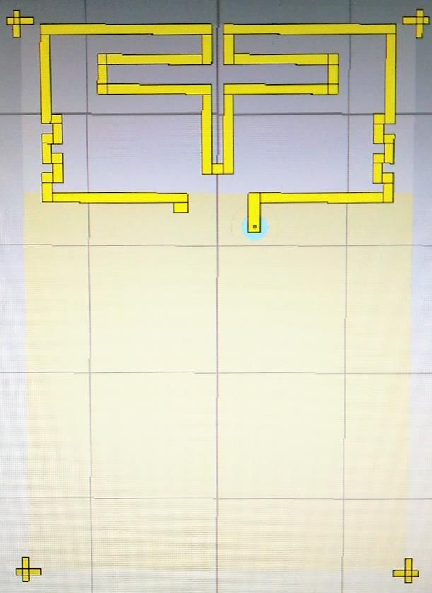
Figure 3.1. Folded dual-loop antenna design (taken from [1])........................................... 19
Figure 3.2. Fabricated dual-loop antenna (taken from [1]) ................................................ 19
Figure 3.3. Optimized geometry design parameters of the presented dual-loop antenna
(taken from [1]): L1=24.5 mm, W1=3 mm, W2=6 mm, g1=1 mm, g2=8 mm, h=8.8 mm.
............................................................................................................................................ 20
Figure 3.4. Simulated and measured return losses of the presented antenna (taken from
[1]) ...................................................................................................................................... 20
Figure 3.5. First approach front part of the dual loop antenna design................................ 21
Figure 3.6. First approach back part of the dual loop antenna design ................................ 21
Figure 3.7. First approach complete front part of the dual loop antenna design ................ 21
Figure 3.8. First approach complete back part of the dual loop antenna design ................ 21
Figure 3.9. Antenna´s feeding point A and ground point B ............................................... 22
Figure 3.10. Coaxial cable´s 50 Ω impedance parameters ................................................. 22
Figure 3.11. Coaxial parameters checked with an online calculator for Zo= 50 Ω............ 23
Figure 3.12. Antenna´s S11 parameter in dB ..................................................................... 24
Figure 3.13. Antenna´s 50 Ω coaxial structure ................................................................... 24
Figure 3.14. Waveguide port definition ............................................................................. 25
Figure 3.15. First antenna redesign .................................................................................... 26
Figure 3.16. S11 parameter after the first optimization ..................................................... 26
Figure 3.17. Schematic PCB module for the proposed antenna ......................................... 27
7Figure 3.18. “Company 1” S11 results for the existing solution with different protections
............................................................................................................................................ 27
Figure 3.19. Second optimization approach, complete front part of the dual-loop antenna
design.................................................................................................................................. 28
Figure 3.20. Second optimization approach, front lateral part of the dual-loop antenna
design.................................................................................................................................. 28
Figure 3.21. S11 parameter after the second optimization ................................................. 29
Figure 3.22. S11 parameter achieving low band operating point ....................................... 29
Figure 3.23. Coloured scale for current intensity from the feeding cable to the antenna
structure .............................................................................................................................. 30
Figure 3.24. Third optimization approach, complete front part of the antenna design ...... 30
Figure 3.25. Third optimization approach, complete back part of the antenna design ...... 30
Figure 3.26. Third optimization approach, front lateral part of the antenna design ........... 31
Figure 3.27. Third optimization approach, back lateral part of the antenna design ........... 31
Figure 3.28. Schematic: Antenna new structure optimization rules. .................................. 31
Figure 3.29. Parameter list used for the final antenna design ............................................ 32
Figure 3.30. S11 parameter for the final antenna design .................................................... 33
Figure 3.31. Final front part of the antenna design without casing .................................... 34
Figure 3.32. Final back part of the antenna design without casing .................................... 34
Figure 3.33. Final front lateral part of the antenna design without casing ......................... 34
Figure 3.34 Final back lateral part of the antenna design without casing .......................... 34
Figure 3.35. S11 parameter for the final antenna design with no resin .............................. 35
Figure 4.1. Autocad model result exported from CST ....................................................... 36
Figure 4.2. How to export from CST to Gerber format in 2D ........................................... 36
Figure 4.3. Antenna final design with markers on the substrate’s corners......................... 37
Figure 4.4. Front.gbr and bottom.gbr from our antenna design ......................................... 37
Figure 4.5. FR4 material (taken from www.alibaba.com) ................................................. 38
Figure 4.6. PCB layer description (taken from www.blackstick.co.uk)............................. 38
Figure 4.7. SMA Female connector taken from (www.lowpowerlab.com) ....................... 38
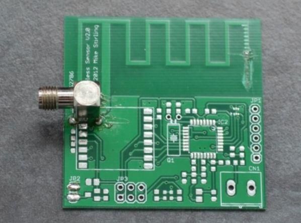
Figure 4.8. Front part of the fabricated dual-loop antenna design ..................................... 38
Figure 4.9. Back part of the fabricated dual-loop antenna design ...................................... 38
Figure 4.10. Completed antenna prototype (with the resin casing), fabricated at UPC
University, Catalonia, Spain ............................................................................................... 39
8Figure 5.1. S11 parameter for the fabricated final antenna ................................................ 41
Figure 5.2. S11 parameter for the “Company 1” actual antenna ........................................ 42
Figure 5.3. “Company 1” S11 results for the existing solution with and without different
protections .......................................................................................................................... 43
Figure 5.4. S11 parameter for the “Company 2” actual antenna ........................................ 44
Figure 5.5. S11 parameter for the complete presented antenna ......................................... 44
Figure 5.6. Anechoic chamber effect ................................................................................. 45
Figure 5.7. Anechoic chamber at UPC University, Catalonia, Spain................................. 45
Figure 7.1. Radiation pattern cuts at 900 MHz of the “Company 1” actual antenna ......... 50
Figure 7.2. “Company 1” actual antenna front view of the radiation pattern at 900 MHz ....
............................................................................................................................................ 51
Figure 7.3. Radiation pattern cuts at 1790 MHz of the “Company 1” actual antenna ....... 51
Figure 7.4. “Company 1” actual antenna front view of the radiation pattern at 1790 MHz ..
............................................................................................................................................ 52
Figure 7.5. Radiation pattern cuts at 2000 MHz of the “Company 1” actual antenna ...........
............................................................................................................................................ 52
Figure 7.6. “Company 1” actual antenna front view of the radiation pattern at 2000 MHz ..
............................................................................................................................................ 53
Figure 7.7. Radiation pattern cuts at 850 MHz of the “Company 2” actual antenna ......... 53
Figure 7.8. “Company 2” actual antenna front view of the radiation pattern at 850 MHz ....
............................................................................................................................................ 54
Figure 7.9. Radiation pattern cuts at 1930 MHz of the “Company 2” actual antenna ...........
............................................................................................................................................ 54
Figure 7.10. “Company 2” actual antenna front view of the radiation pattern at 1930 MHz
............................................................................................................................................ 55
Figure 7.11. Radiation pattern cuts at 2150 MHz of the “Company 2” actual antenna .........
............................................................................................................................................ 55
Figure 7.12. “Company 2” actual antenna front view of the radiation pattern at 2150 MHz
............................................................................................................................................ 56
Figure 7.13. Radiation pattern cuts at 850 MHz of the antenna with resin ............................
............................................................................................................................................ 56
9Figure 7.14. Antenna with resin front view of the radiation pattern at 850 MHz ..................
............................................................................................................................................ 57
Figure 7.15. Radiation pattern cuts at 1720 MHz of the antenna with resin ..........................
............................................................................................................................................ 57
Figure 7.16. Antenna with resin front view of the radiation pattern at 1720 MHz ................
............................................................................................................................................ 58
Figure 7.17. Radiation pattern cuts at 2150 MHz of the antenna with resin ..........................
............................................................................................................................................ 58
Figure 7.18. Antenna with resin front view of the radiation pattern at 2150 MHz ................
............................................................................................................................................ 59
List of Tables
Table 5.1. Directivity measures of the analysed antennas (“Company 1” actual antenna,
“Company 2” actual antenna, and our proposed antenna with resin), at three different
frequencies.......................................................................................................................... 47
Table 5.2. Gain and efficiency measures in dB of the “Company 2” actual antenna and our
proposed antenna with resin, at three different frequencies ............................................... 47
101. Introduction
1.1. Introduction to the Internet of Things (IoT)
Nowadays, our everyday life is surrounded by wireless devices and artefacts that
can be connected with an on and off switch to the Internet. These systems of
interconnected devices, which are embedded with electronics, sensors, actuators and
software to exchange and collect data, are what is called The Internet of Things (IoT).
Therefore, every common object such as the appliances at home, clothes and furniture
among others, can communicate the information required becoming both more
“intelligent” and independent.
In the field of electromagnetism, to develop small size antennas to be integrated within
sensor devices is key to realize the data transmission while being able to place the device
anywhere, providing a faster, smoother and cheaper flow of information.
For this reason, a limiting factor in modern electronics is that large antennas are not
compatible with electronic circuits, which are shrinking everyday.
Other obstacles associated with the IoT include providing reliable connectivity and
maintaining reasonably performance with a compact antenna size, despite being sited in
the most challenging environments for radio propagation.
To this end, antenna design with some desirable features such as multiband operation, low
profile, light weight, and easy fabrication have earned high attention for practical
applications.
1.2. Requirements and specifications
The network topology of IoT systems is composed of simple nodes or devices
which sense, gather and transmit a certain amount of information to a gateway or central
controller that provides the Internet and cloud services connectivity.
Communication between nodes and a centralized “cloud” must be secure in order to
protect and process the data stored, enabling the sensor devices to bounce actionable
information down to humans. Moreover, these nodes and gateways must be designed in
order to keep the power consumption at its minimum as well as providing a large wireless
connectivity range.
11Thus, in order to deploy networks of IoT devices, both the network and the antenna must
be specified, which means that the type of wireless network to be used for connectivity
should be determined, and consequently, the antenna (or multiple antennas) needed to
comply with the device´s design and physical properties. For instance, 900MHz, 2.4GHz
and 5GHz radios may all have different requirements for the antenna design.
The following subsection focuses on this last part, covering IoT antennas of various types
that will help IoT module designers to make the right choice of antenna, which is of
interest for the purpose of this project.
1.2.1. Antenna types for the IoT
IoT devices are usually very small and ubiquitous, for this reason, compact size,
low-power consumption and high reliability are the three main factors to take into account
in the antenna design.
If the physical space is a priority, the design to implement is commonly the prefabricated
chip antennas, which is relatively easy to realize and cost effective when produced in high
volumes. Chip antennas (see Figure 1.1) are surface-mount devices used for frequencies
that range from 300 MHz to 2500 MHz with a size that goes from 2 up to 20 square
millimetres in length, becoming the smallest design available.
They are manufactured on ceramic substrate or a small multi-layer Printed Circuit Board
(PCB), which acts as the antenna ground and occupies half of the antenna system, the chip
itself constitutes the other half.
However, chip antennas have a very narrow bandwidth, are strongly dependent on the
ground plane, and must be made to the exact frequency.
Figure 1.1. Embedded ceramic multi-band Figure 1.2. PCB antenna with test port
chip antenna (taken from Pulse Electronics News). attached (taken from Mike´s Lab Notes).
If the IoT devices contain multiple sensors and are meant for large-scale manufacturing,
reduced unit cost and reasonable design flexibility will be considered significant matters.
12In these cases, PCB antennas are regarded as the best option, with advantages that stem
from the PCB´s highly refined manufacturing process.
PCB antennas (see Figure 1.2) perform well above 800 MHz and have a small size at high
frequencies; performance challenges appear below 500 MHz, the size increases as the
frequency decreases. It must be borne in mind that multiple antennas increase the PCB
size and, redesigning the antenna requires redesigning the board as well.
PCB antennas can have a meandered conductor design, which means having a trace in a
certain pattern on the circuit board, or they can be planar monopole. The typical types of
printed antennas include patch antennas, inverted-F antennas (IFA), or planar inverted-F
antennas (PIFA) (see Figure 1.3). Among their benefits it can be seen that the space taken
by a PCB is less than by a dipole antenna (see Figure 1.4) due to using the ground plane of
the circuit board to help them radiate. Variants include flexible printed circuit (FPC) and
stamped metal antennas.
Figure 1.3. PIFA antenna (taken from Figure 1.4. Fine-tuned dipole antenna
Richard Langley thesis on PIFA antenna). (taken from Flytron).
The following option in terms of performance would be to source a proprietary antenna,
which is custom-designed in order to meet the desired specifications. In this case, it´s
critical to know the exact use case for the antenna to completely describe and design the
performance dynamics, enabling the antenna to be designed for maximum efficiency. One
of the main drawbacks of choosing proprietary antenna designs is the cost, which can be
reduced if using a pre-tuned standard antenna that can be integrated onto a PCB assembly
while ensuring high quality.
In those cases where the budget is tight, a fair option is the wire antenna (see Figure 1.5).
Wire antennas increase in size by a decrement in frequency and require more testing and
simulation regarding electromagnetic performance. However, several wire antennas can be
attached to a module board via micro-coaxial cable, which makes them suitable when
multiple wireless technology transceivers are needed for the IoT device. Also, the
prototype design is very cost effective and allows for several tested versions during its
development.
13Nevertheless, a tradeoff between maximum performance and price can be found in the
whip antennas (see Figure 1.6). Even though they are external and require a connector to
the PCB module, interferences when dealing with multiple transceivers can be avoided.
Figure 1.5. A wire antenna kit with a coil Figure 1.6. Sennheiser A182 whip antenna
of wire, strain insulators and a balun for Evolution Series (Frequency B).
(taken from Wikipedia).
Finally, it must be noticed that higher frequency systems are preferred in terms of space
limitations since the higher the frequency, the lower the wavelength and thus, a more
compact antenna design is doable at a cost of reducing the distance that lower frequencies
achieve for communication. In practice, many IoT applications prefer the 868 MHz band
in Europe and the 915 MHz band in the USA; in these bands the propagation is more
reliable and the wavelength is larger than 30 cm (at the speed of light c, the wavelength is
given by λ=c/f).
Furthermore, when selecting between an external antenna, or embedding one into the
module itself, designers must consider the material and the potential placement of the
product regarding how difficult it is to get a wireless signal from the nearest gateway.
1.3. Motivation and statement of purpose
As “International Journal of Antennas and Propagation” explains in [2], according
to analysts, the Internet of Things´ number of connected devices is increasing impressively,
rising the figure of 50 billion devices and enabling the emergence of new smart objects
that operate at different frequency bands, bandwidths and power levels.
With this technology boom comes the need to provide the wireless communication
systems with reliable data transmission, which requires advanced investigation in the field
14of antenna design. Therefore, the electromagnetic properties of the environment, where
the smart devices that gather the data are placed, must be taken into account during the
antenna modelling.
In this aspect is where the thesis focuses, realizing a PIFA antenna design and
optimization in an IoT framework, finding a compromise between performance and size
while minding the fabrication price. The goal is to achieve the same performance as
existing solutions while reducing the cost and size significantly.
The already marketed solution to compare with, consists of a PCB module with an
external pentaband antenna that covers the frequency bands:
- 824.4 to 960 MHz
- 1710 to 2170 MHz.
Where the PCB module is 60(L) x 70(W) mm2 and it´s located inside a casing with the
following measures (see Figure 1.7):
Figure 1.7. Existing solution´s PCB module and its casing.
In this project, the proposed PIFA antenna covers the same frequency bands by means of a
dual-loop design with a compact size, which is compatible with the existing sensor device.
In addition, it is embedded in the casing along with the PCB module, complying in this
way with the IoT requisites.
15The purpose of the proposed system, as well as of the existing system, is to gather and
process through the sensor device the data collected of a garbage container in order to
know whether it has reached its maximum level among other information. This is very
useful when it comes to deploy a whole network of these sensors, actively storing and
transmitting information in real time, which can be used to take action in a certain area or
have a dynamic route for the dustmen while working, prioritizing the places where there is
more waste accumulated. Moreover, this functionality helps to communicate whether any
of the containers is having any kind of trouble such as cathing on fire, scrolling down or
being placed upside down by anyone.
Last but not least, this antenna design can be used in any sensor that requires an antenna to
communicate its data in an efficient way at an affordable price, having the properties of
scalability to a network of sensor devices and a compact size to fit almost anywhere within
its embedded system.
1.4. Project scope
The scope of this project is to simulate and optimize an alternative antenna design
to be embedded within a sensor device in a resin casing in order to realize the same
functions as an existing external antenna but at less cost and size, without compromising a
good performance. The objectives to be achieved are:
• Design an efficient alternative IoT antenna to be integrated within sensors.
• Optimize the design in order to achieve the frequency bands’ requirements with
10 dB return loss during the simulations.
• Repeat the process taking into account the casing effects of the device and how it
affects the system’s electromagnetic behaviour.
• Get the antenna fabricated in order to take real measurements of its performance
and compare the results with the simulations.
• Redo the measurements with the antenna inside the resin casing and compare to
both the simulations and the existing solutions (actual example taken, from
“Company 1”, and its competitor’s solution, from “Company 2”).
• Analyse all the results and present the conclusions. See whether they meet our
original expectations.
161.5. Thesis organisation
This document is organized in chapters with the following content:
• Chapter 1: Starts with an introduction to the Internet of Things (IoT), followed by
the requirements and specifications for each antenna type in the IoT framework,
motivation and statement of purpose, project scope and thesis organisation.
• Chapter 2: with the objective to review what has previously been done in this
research field, a state of the art of the technology used or applied in this thesis is
presented.
• Chapter 3 explains in detail the methodology and project development carried out
during the process of fulfilling the goals mentioned in the project scope, highlighting the
initial steps that every design must take: antenna modelling, structure and ports among
others. An optimization process coexists with the design stage.
• Chapter 4: the fabrication process and specifications for the antenna are
commented. Also, the implementation changes made from the final simulated design, and
the environmental impact.
• Chapter 5 addresses the analysis of the results obtained by measuring the
available antennas and its comparison with the results that appeared in the simulation.
• Chapter 6: last conclusions are drawn to summarize the project results and
contributions. Future steps related to the project are underlined as well as its practical
applications.
• Chapter 7 is constituted by the appendix, which includes all the radiation
diagrams from section 5.2.
172. State of the art
The growth in the antenna design field has exploded with the rapid evolution of
communication technologies. Many studies have been carried out within this aspect such
as [4] where a built-in folded monopole antenna is modified and analysed so as to get a
small size, good performance and low profile by folding a loop element sideways.
Moving on to [5], a compact antenna size is achieved for mobile handsets using a feeding
strip, shorting strip and a folded loop radiating element with embedded tuning notches.
Same goal is addressed by [6]-[8] employing an internal antenna with a bent-shaped
structure for multiband operation implementation in handset devices.
With regards to [9], a broadband internal antenna formed by a combination of a shorted
monopole and a loop type antenna is proposed. Despite being small and having a simple
structure, it performs with wide impedance bandwidths, high antenna gains and good
radiation patterns. A FR4 substrate is used with 1mm thickness and 4.4 relative
permittivity.
In addition, another research has been carried out in [10], where a hybrid loop/monopole
slot antenna for quad-band operation in mobile phone devices is proposed. It is composed
by a monopole slot antenna and a meandered loop antenna operating at GSM/DCS/
PCS/UMTS systems, covered by two wide bands centred at 900 and 1900 MHz.
However, the above mentioned designs cannot be easily embedded inside a sensor device
because of their large size. For this reason, our proposed antenna is mainly based on [1],
using its results as a first approach to a better final design that really meets our
specifications.
In [1], a compact folded dual-loop antenna for mobile handset applications is designed
using a bent-shaped radiator, which consists of a pair of symmetric meander strips of
small size (50(L) x 9(W) x 9(H) mm3). This antenna design can be tuned by modifying the
spaces g1 and g2 between the loops, achieving with its compact size the desired frequency
bands covering 847–971 and 1670–2230 MHz. Thus, becoming a good option for
integration within mobile handsets as an internal antenna.
Our project contribution to the state of the art in this field is to develop and modify the
approach taken in [1] for mobile devices to provide with an internal antenna that can be
embedded in sensor devices such as the one taken as an example from “Company 1”. Not
only a compact and simple structure is achieved but also it is more cost-efficient than the
existing solutions as it will be seen in the following sections. The wider impedance
bandwidth obtained in comparison with the already marketed antennas is a huge benefit to
consider as well.
183. Methodology / project development
3.1. Antenna design
3.1.1. Baseline design
In [1], the geometry of the presented folded dual-loop antenna (see Figure 3.1),
consisting of a pair of symmetric meander strips, is designed with 1 mm union width using
0.2-mm-thick copperplate. The two loops that form the radiator are then bent, resulting in
two perpendicular layers so as to achieve a compact size. As a consequence, the antenna
final dimensions are just: 50(L) x 9(W) x 9(H) mm3.
Regarding the ground plane, the same copperplate from the antenna is used with a size of
90(L) x 50(W) mm2, which simulates the ground plane for general handset devices. In
order to hold a mobile casing, a vertical shielding plane is used and connected to the
ground plane (see Figure 3.2).
Figure 3.1. Folded dual-loop antenna design Figure 3.2. Fabricated dual-loop antenna
(taken from [1]). (taken from [1]).
For multiband operation, the longer loop (path A–C–D–E–F–G–H–I–B), (see Figure 3.3),
works for the lower band and corresponds to one wavelength at 900 MHz. Working for
the upper band, the shorter loop (path A–C–D–F–H–I–B) corresponds to one wavelength
at 1800 MHz.
Furthermore, two gaps g1=1 mm, and g2=8 mm are designed to obtain good radiation and
enable operating frequency tuning respectively.
19Figure 3.3. Optimized geometry design parameters of the presented dual-loop antenna (taken from
[1]): L1=24.5 mm, W1=3 mm, W2=6 mm, g1=1 mm, g2=8 mm, h=8.8 mm.
The fabricated prototype for the baseline design (see Figure 3.2) was measured and tested,
resulting in two impedance bandwidths with 6 dB return loss that satisfy the
GSM/DCS/PCS/UMTS bands’ requirements around 847–971 and 1670–2230 MHz (see
Figure 3.4).
Figure 3.4. Simulated and measured return losses of the presented antenna (taken from [1]).
3.1.2. First approach
Taking into account the purpose and advantages of [1], a first design is realised to
obtain the first simulation results that will lead to changes and advances to get closer to
meet our desired specifications. A specialist tool for 3D electromagnetic simulation of
high frequency components, CST Microwave Studio, has been used for an accurate
analysis of the proposed antenna.
20Thus, the first approach taken in the design (see Figures 3.5 and 3.6) has the same size and
parameters as in [1], but instead of realizing a bent-shaped structure, it has been left plain
flat on a FR4 substrate with 2(W) mm more than the surface dimensions from Figure 3.1
50(L) x 70(W) mm2, plus the antenna dimensions 50(L) x 18(W) mm2. The substrate,
which is placed in between the antenna and the copper ground plane, has therefore the
total dimensions of 50(L) x 90(W) mm2. The copper ground plane constitutes the bottom
layer in our design and its measures are the same as in Figure 3.1 plus 2(W) mm, which is,
in total, 50(L) x 72(W) mm2 (see Figures 3.7 and 3.8).
Figure 3.5. First approach front part of the Figure 3.6. First approach back part of the
dual-loop antenna design. dual-loop antenna design.
Figure 3.7. First approach complete front part Figure 3.8. First approach complete back
of the dual-loop antenna design. part of the dual-loop antenna design.
21As you can see from the above pictures, our choice for the IoT antenna realization to be
embedded in a PCB module with its casing, which is designed at the end of this chapter, is
a PIFA antenna type. Our PIFA antenna contains the baseline design’s meander strips in
order to achieve the desired small size, at the cost of slightly reducing the fractional
bandwidth.
However, unlike in the design made at [1], a balun to be connected between the feeding
cable and the antenna won´t be used in the construction and testing of the proposed
antenna. Instead, just a coaxial cable is employed and connected to the antenna feeding
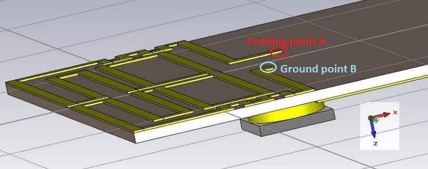
point A (see Figure 3.9). It should be noticed as well that the strip corresponding to the
feeding point A is enlarged and connected to the ground copper plane through the selected
substrate (FR4) via the chosen coaxial cable.
Figure 3.9. Antenna´s feeding point A and ground point B.
When performing the design, it should be taken into account that one of the most powerful
characteristics of CST it that the 3D models are parametric. This is particularly useful
when optimizing the antenna since it is enough to change the value of these parameters to
change the dimensions of the antenna model, without redoing or manually adjusting the
whole design.
As mentioned before, a coaxial (feeding structure) composed of an inner conductor, a
dielectric and an outer conductor was included in CST to excite our antenna. Each one of
the elements was created using the cylinder creation mode. The parameters needed to
specify the radius of the cylinders and their length were the following:
Figure 3.10. Coaxial cable’s 50 Ω impedance parameters.
22In Figure 3.10, CoaxL is the coaxial’s length, from 0 to Coax_r is the inner conductor,
from Coax_r to CoaxR is the dielectric and, from CoaxR to CoaxR3 is the outer conductor.
The dimensions for the coaxial’s structure (Coax_r, CoaxR and CoaxR3) were obtained in
order to get a 50 Ω impedance matching following the next formula:
Where Er (relative permittivity) has the value of 2.1 for the Teflon material of the
coaxial´s dielectric. Also, Coax_r is equal to half the value of d, CoaxR is equal to half the
value of D and, D/d= 4.02/1.2= 3.35, which is one of the combinations that verify a
characteristic impedance Zo= 50 Ω for the respective Er and, its measures are
approximated to the size of some marketed connectors.
Furthermore, these values can be checked with an online coaxial impedance calculator
such as the one in [11] (see Figure 3.11).
Figure 3.11. Coaxial parameters checked with an online calculator for Zo= 50 Ω.
Being D1= d= 2*Coax_r= 1.2 mm; and D2= D= 2*CoaxR= 4.02 mm.
Once the proper first approach design has been achieved, its electrical characteristics and
radiation performance are analysed by obtaining the simulation of the antenna´s reflection
parameter (S11) in dB as appears in the next screenshot (see Figure
233.12):
Figure 3.12. Antenna´s S11 parameter in dB.
It can be observed that there are three main resonant frequencies at around 750 MHz, 1400
MHz and 2200 MHz, which is not what we wanted but a good first simulation result in
order to optimize and get the desired outcomes. It is expected to be different from the
baseline designed simulation (see Figure 3.4) due to the changes applied and deviations
regarding the material properties and the substrate layer.
Note: in CST the coaxial port should be declared, this means it is necessary to add the
excitation port to the antenna device, for which the reflection parameter is later calculated.
The port simulates an infinitely long coaxial waveguide structure that is connected to the
structure at the ports plane (see the definition process in Figures 3.13 and 3.14).
Figure 3.13. Antenna´s 50 Ω coaxial structure.
24Figure 3.14. Waveguide port definition.
3.1.3. First optimization
The antenna optimization consists of a first stage of trial and error where we detect
how the different parameters influence the antenna’s behaviour. As a first practical
method, it can be proven that, in order to position a resonant frequency in a different
operational frequency, the following rule applies:
The new chosen antenna length is the antenna´s current length times the current resonant
frequency over the desired resonant frequency.
New_L= Current_L*Current_freq/ Desired_freq
With this rule, the length that the antenna must have in order to achieve the expected
resonant frequency can be calculated given the non-desired current values of the antenna’s
length and operational frequency.
Moreover, changing the value of g1 implies a change in the low frequency levels
(reducing the g1 value, places the antenna’s low-band operational point even lower in
frequency) and, incrementing carefully the g2 value contributes to a better performance in
the high frequencies due to a reduction of the ripples that appear in the Figure 3.12 S11
parameter’s graphic.
Thus, for the first set of final values (see Figure 3.15):
- Antenna Total Length= 34 mm.
- Antenna Total Width= 18 mm (same value as before).
- g1= 1.5 mm.
- g2= 11 mm.
The following S11 parameter graphic is obtained (see Figure 3.16). It can be seen that
with the new parameter configuration the expected wideband properties are obtained
around the wanted frequencies, which are located in the 800-1000 MHz band and 1800-
2000 MHz band. Also, the ripples presented in the upper band from Figure 3.12 are now
smoother.
25Figure 3.15. First antenna redesign.
Figure 3.16. S11 parameter after the first optimization.
3.1.4. Second approach
In this second procedure, the current basic design that works properly and meets
the requirements is transformed in order to achieve “Company 1” existing solution’s
performance while fulfilling the company´s requisites for our proposed antenna.
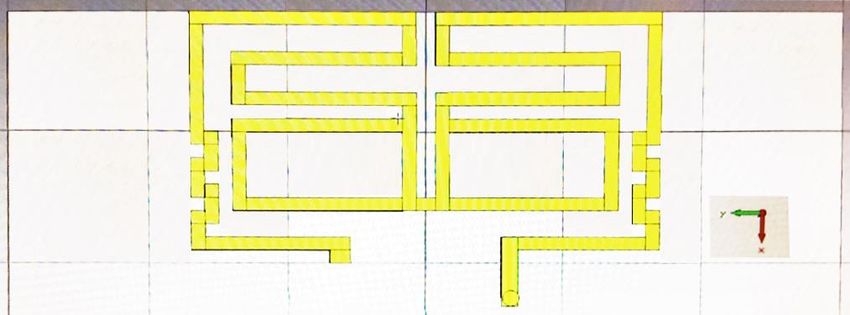
Firstly, the “Company 1” schematic (see Figure 3.17) where the antenna will be placed,
determines the new substrate and copper ground plane dimensions. Thus, the current
substrate size is 60(L) x 85(W) mm2, which includes the space where the antenna is
located. The current copper ground plane size is 60(L) x 85(W) mm2 minus the width of
the antenna, which is 18(W) mm prior optimization, giving a total of 60(L) x 67(W) mm2.
The copper ground plane width is, therefore, dynamic, and changes depending on the
current antenna width, which will be modified along with the other parameters to fit the
established requirements.
26Figure 3.17. Schematic PCB module for the proposed antenna.
Secondly, another major change that takes place is the integration of the device’s casing,
filled with resin, which also modifies the reflexion coefficient result of the antenna
performance. The resin material has a relative permittivity Er= 3 and a tangent loss of 0.04.
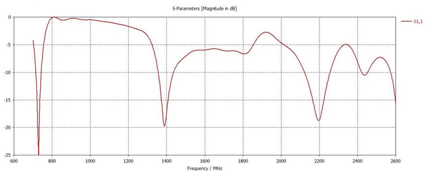
As expected, the first simulation of the second approach does not comply with the
requirements set by the existing solution behaviour (see Figure 3.18) and, for this reason,
we directly move on to the next optimization iteration.
Figure 3.18. “Company 1” S11 real tested results for the
existing solution with different protections.
273.1.5. Second optimization
Following the steps taken in “First optimization”, several parameter combinations
were tried, applying the before mentioned rule (New_L= Current_L*Current_freq/
Desired_freq) as a guideline to place the resonant frequencies in their desired place along
with a trade-off between the other design values.
However, in this case, it was not possible to find a suitable performance within the given
design (see Figures 3.19 and 3.20) from the second approach, as the final simulation (see
Figure 3.21) shows by not meeting the requirements of Figure 3.18.
Figure 3.19. Second optimization approach, Figure 3.20. Second optimization approach,
complete front part of the dual-loop antenna front lateral part of the dual-loop antenna design.
design.
Figure 3.21 represents the best overall performance that could be found regarding the
reflection coefficient during the second optimization stage. It was acquired by giving to
each of the next listed parameters the subsequent measures:
- Antenna Total Length= 58 mm.
- Antenna Total Width= 18 mm (same value as before).
- g1= 2 mm.
- g2= 15 mm.
28Figure 3.21. S11 parameter after the second optimization.
As a consequence, it was decided to split up the optimization task by aiming at obtaining
first the low band resonant frequency, leaving the achievement of the upper band resonant
frequency for the following subchapter.
Obtaining our first goal (see Figure 3.22), by moving down in frequency (around 900
MHz) the low band antenna operation point situated at 1000 MHz in figure 3.21, was
relatively easy to obtain. The new values for the design parameters are:
- Antenna Total Length= 56 mm.
- Antenna Total Width= 22 mm.
- g1= 1 mm.
- g2= 14 mm.
Figure 3.22. S11 parameter achieving low band operating point.
29The most difficult part, meeting the specifications in the upper frequency band without
significant ripples, is a challenge that will be overcome in the following paragraphs.
3.1.6. Third optimization
To completely obtain the desired results, we went one step further by analysing the
currents that take place in the antenna, which emerge from the H-plane coaxial’s TEM
mode. Placing monitors in the frequencies from figure 3.22 that we want to get rid of, such
as the highest one at 2400 MHz, allows seeing in red colour (see Figure 3.23) the antenna
strips where the current flows are more intense. Those are the ones we should redesign to
achieve a suitable behaviour.
Figure 3.23. Coloured scale for current
intensity from the feeding cable to the
antenna structure.
Thus, it could be observed that the strips corresponding to the paths E and G, were causing
the unwanted performance, they had intense currents at the undesired frequencies. Once
this information was available, we proceeded to eliminate the corresponding strips and
simulate the new structure (see Figures 3.24, 3.25, 3.26 and 3.27).
Figure 3.24. Third optimization approach, Figure 3.25. Third optimization approach,
complete front part of the antenna design. complete back part of the antenna design.
30Figure 3.26. Third optimization approach, Figure 3.27. Third optimization approach,
front lateral part of the antenna design. back lateral part of the antenna design.
3.1.6.1. Useful rules for optimization
When carrying out the simulations in the redesigned antenna, two useful
statements can be derived and employed any time with, at least, this new proposed
antenna. Thus, for the remain strips that compose the antenna’s inner loop, whose path
corresponds to D and H from Figure 3.3, the following rules apply (see Figure 3.28):
Figure 3.28. Schematic: Antenna new structure optimization rules.
31- First rule: the more the vertical strip is moved from path D to the left, along with
the symmetrical movement of the vertical strip H to the right, the resonant
frequency of the upper band moves proportionally to the right (the upper band
operational frequency increases) in the S11 graphic.
- Second rule: the more the vertical strip is moved from path D to the right, along
with the symmetrical movement of the vertical strip H to the left, the resonant
frequency of the upper band moves proportionally to the left (the upper band
operational frequency decreases) in the S11 graphic.
3.2. Final antenna design and optimization
Applying the second and third optimizations along with an overall improvement,
by considering the impact of modifying the rest of the parameters’ values, led to the
following design characteristics (see Figure 3.29):
- Antenna Total Length= 54 mm.
- Antenna Total Width= 26.8 mm.
- g1= 1.8 mm.
- g2= 9.2 mm.
Figure 3.29. Parameter list used for the final antenna design.
This final optimization process took place as follows:
- First, based on the third optimization structure, it was found that for a 2.4 mm
difference in distance to the left for path D and right for path H (First rule), the
main specifications were approximately achieved, such as the resonant frequency
points and a good radiation performance. Thus, both the low-band and upper-band
resonant frequencies were accomplished.
32You can also read