Single Event Latch-up Testing - Advanced Analog to Digital Converter ADC14155W-MLS
←
→
Page content transcription
If your browser does not render page correctly, please read the page content below
Single Event Latch-up Testing
Advanced Analog to Digital Converter
ADC14155W-MLS

                  Literature Number: SNAA153
National Semiconductor Corporation
                                  2900 Semiconductor Drive              +1 408 721 5000 Tel
                                  Santa Clara, CA 95052-8090 USA        www.national.com

       Single Event Latchup Testing
    Advanced Analog to Digital Converter
             ADC14155W-MLS

                  Hi-Rel Operations
            Radiation Engineering/RHA Programs
                   2900 Semiconductor Dr.
                    Santa Clara, CA 95052

Date: August 02, 2006

Product Engineer: Kevin Nguyen
Supervisor: Rob Rennie
Phone # : +1 (408) 721-50503
email ID: kevin.nguyen@nsc.com

                        1 of 12                                        Rev. B
National Semiconductor Corporation
                                       2900 Semiconductor Drive                +1 408 721 5000 Tel
                                       Santa Clara, CA 95052-8090 USA          www.national.com

Table of Contents                                                           Page

      1.0    Objective                                                        3
      2.0    Conclusion                                                       3
      3.0    Summary                                                          3
      4.0    Test Data                                                        3
      5.0    Description of Product                                           3
      6.0    Test Method                                                      4
      7.0    Description of Test Setup                                        4
      8.0    Test Plan and Procedures                                         5
      9.0    Test Facility and Personnel                                      7
      10.0   Test Equipment                                                   7
      11.0   Appendix – Heavy-Ion Curves and Table                            9
      12.0   Test Log Tables                                                  11

                             2 of 12                                          Rev. B
National Semiconductor Corporation
2900 Semiconductor Drive +1 408 721 5000 Tel
Santa Clara, CA 95052-8090 USA www.national.com
1.0 Objective
To evaluate the SEL (Single Event Latchup) performance of ADC14155W-MLS, to measure
the SEL cross section vs. the effective LET (Linear Energy Transfer) to the maximum
cross section and effective LET possible at the experimental facility of use, or to verify
that the part is immune to SEL for effective LET’s up to 121 MeV/mg/cm2.
2.0 Conclusion
The Space Level version of the ADC14155 is immune to SEL with LET’s up to 121.89
MeV/mg/cm2.
3.0 Summary
No latchup was observed on any of the 3 DUT’s (Devices Under Test), at room and hot
temperatures, with Bi209 at 0° incident angle, LET = 99.85 MeV/mg/cm2 at the surface of
the Silicon. The incident angle was increased to 35°, LET = 121.89 MeV/mg/cm2 at the
surface of the Silicon, and again no latchup was seen on the 3 DUT’s at both room and
hot temperatures.
4.0 Test Data
See Tables 1, 2 and 3 on pages 9 & 10 for SEL Data taken on the 3 DUT’s.
5.0 Description of Product
The ADC14155W-MLS is a high-performance CMOS analog-to-digital converter capable of
converting analog input signals into 14-bit digital words at rates up to 155 Mega Samples
Per Second (MSPS). This converter uses a differential, pipelined architecture with digital
error correction and an on-chip sample-and-hold circuit to minimize power consumption
and the external component count, while providing excellent dynamic performance. A
unique sample-and-hold stage yields a full-power bandwidth of 1.1 GHz. The ADC14155W-MLS
operates from dual +3.3V and +1.8V power supplies and consumes typically 974 mW of
power at 155 MSPS. The separate +1.8V supply for the digital output interface allows
lower power operation with reduced noise. A power-down feature reduces the power
consumption to 5 mW with the clock input disabled, while still allowing fast wake-up
time to full operation.
The ADC14155W-MLS Space Level die was used for the DUT’s. The die was placed in a
decapsulated plastic package to facilitate SEL (Single Event Latchup) testing.
3 of 12 Rev. BNational Semiconductor Corporation
2900 Semiconductor Drive +1 408 721 5000 Tel
Santa Clara, CA 95052-8090 USA www.national.com
6.0 Test Method
JESD57 (EIA/JEDEC Standard No. 57), “Test Procedures for the Measurement of Single
Event Effects in Semiconductor Devices from Heavy Ion Irradiation” was strictly
adhered to for test procedures and definitions (available at http://www.jedec.org/). ESCC
25100 was also used as a reference, and, as closely as possible, was adhered to (available
at https://escies.org/public/radiation/esa/standards.html). JESD57 defines the
requirements and procedures for Earth based SEE testing of integrated circuits. The test
method is only valid when using a Van de Graaff or Cyclotron Accelerator. This method
does not apply to SEE testing that uses neutrons, protons and other lighter particles. This
test method assumes that the accelerator test facility has the ability to mount and position
the DUT in a vacuum chamber, provide heavy ion dosimetry; etc. Inquiries and visits to
the site have verified that this is indeed the case. All DUT's must be decapsulated.
7.0 Description of Test Setup
The test circuit for the ADC14155W-MLS consisted of the ADC14155 evaluation board
connected to a WaveVision 4 data capture board, driven by WaveVision 4 software. The
two boards were secured to the vacuum chamber fixture and powered up by two separate
power supply sources.
The ADC evaluation board delivers conversion data along with a source-synchronous
clock to the FPGA device on the WaveVision 4 board via a Future Bus connector.
A personal computer was connected to the WaveVision 4 board for communication,
control, and data gathering. Data and events were uploaded to the personal computer after
every run (exposure to accelerated ions) and after every power up sequence to make sure
the DUT was still operating correctly.
For SEL testing the input was a slowly varying sine wave of approximately 1MHz, full
scale and AC coupled through a balun and AC coupling capacitors, 4.7nF. The input
signal was clocked in (sampled) at a frequency of 155 MHz and amplitude of 0 – 3Vp-p.
A current probe was attached to an oscilloscope and was used to monitor the total current
drawn by the evaluation board (which is primarily the sum of the VA and VDR currents
drawn by the DUT).
A latchup event was defined as a sustained increase in DC current drawn by the
evaluation board (which would coincide with an increase in current on either the VA or
VDR power pins of the DUT) that persisted until the part was powered down. A
temperature controller was connected to the thermistors and to the resistive heaters and
4 of 12 Rev. BNational Semiconductor Corporation
2900 Semiconductor Drive +1 408 721 5000 Tel
Santa Clara, CA 95052-8090 USA www.national.com
provided both temperature measurement and heater control for the hot temperature
testing.
8.0 Test Plan and Procedures
8.1 Ions, Angles, Temperatures, and Applied Voltages
The SEL test was started with the heaviest ion available at 0° incident angle (0°
being the beam perpendicular to surface of die) to establish the saturated or
largest cross-sectional area. The lower energy (lighter) ions were to be selected in
descending order, as available, until latchup was no longer observed (below the
threshold of SEL).
The SEL testing was performed at two different temperatures: ~35º C (ambient
temp at “Room Temp” in the vacuum chamber), and 65º C (Hot Temp, as
determined by thermistor attached to the evaluation board in the proximity of the
DUT). VA = 3.3V & VDR = 1.8V was used for all temperatures. The 65°C, as
determined by the thermistor near the DUT , was chosen because it is the
maximum practical temperature that the part can be heated to on an evaluation
board without the adhesive of the heaters melting and falling off the board. Since
the LLP package containing the DUT for these experiments has a θja of 24°C/W
and the power dissipation of the device is documented to be ~940mW, so the
junction temperature was calculated to be 87.56°C (65°C + (24°C/W)*(0.94W) =
87.56°C). Therefore, at “Hot Temp”, the DUT was running at a junction
temperature of approximately 90°C.
Testing was also performed at 35° incident angle, measured from a perpendicular
to the surface, when needed to achieve an effective LET of approximately
120MeV/mg/cm2.
8.2 Power Up / Power Down and Testing Sequence
a) Set up test equipment/circuit, with DUT, and verify correct
operation.
Initial Power Up Sequence:
1) Apply 5.0V to the evaluation board which then
regulates and supply 3.3V to VA and 1.8V to VDR
simultaneously
2) Apply Clock – 155MHz sine wave 0-3.3Vp-p
3) Apply Waveforms to be sampled (see section 7.0 for
description)
Subsequent Power Down Sequences:
5 of 12 Rev. BNational Semiconductor Corporation
2900 Semiconductor Drive +1 408 721 5000 Tel
Santa Clara, CA 95052-8090 USA www.national.com
Power OFF the evaluation board, i.e., remove 3.3V from VA and
1.8V from VDR simultaneously (leave clock signal and inputs
applied and running).
Subsequent Power Up Sequences:
1) Power ON the evaluation board, i.e., apply 3.3V to VA
and 1.8V to VDR simultaneously (leave clock signal and
inputs applied and running).
Final Power Down Sequence:
1) Power OFF the evaluation board, i.e., remove 3.3V
from VA and 1.8V from VDR simultaneously
2) Remove Clock – 155MHz sine wave 0-3.3Vp-p
3) Remove Waveforms being sampled from input pins
b) Check with facility’s personnel for correct ion beam characteristics,
energy, and flux. Ensure detectors are working properly.
c) Power up Device-Under-Test (DUT), using the “Subsequent Power
Up Sequences” step above. Ensure it is operating properly.
d) Expose the DUT to the ion beam.
e) Record all pertinent data after exposure including if DUT latched-
up or not.
f) Power down DUT using the “Subsequent Power Down Sequences”
step above.
g) Repeat steps “b” through “f” for different energies and ion species.
h) Repeat steps “b” through “g” for samples #2 and #3.
i) Repeat steps “b” through “h” at 65°C (case temperature).
j) Power Down as per “Final Power Down Sequence” above.
k) Upon completion, the data was analyzed and this final test report
was generated.
8.3 Other Information Associated with Testing
a) Facility:
Lawrence Berkeley National Laboratory
1 Cyclotron Road
Berkeley, CA 94720
b) Test Method: EIA/JESD 57 – “Test Procedures for the
Measurement of Single-Event Effects in Semiconductor Devices
from Heavy Ion Irradiation”, December, 1996
c) Sample Size: 3
d) Bias Voltage: VA = 3.3V; VDR = 1.8V.
e) Sampling Frequency: 155 MHz
f) Temperatures: ~35ºC (room temperature, no heat applied) and
65ºC (thermistor in close proximity to DUT).
6 of 12 Rev. BNational Semiconductor Corporation
2900 Semiconductor Drive +1 408 721 5000 Tel
Santa Clara, CA 95052-8090 USA www.national.com
g) Selected LET values, see figure 1 (page 8). The facility reserves
the right to change this table. The actual “Cocktail” used was the
4.5MeV/nucleon “Cocktail” as per figure 1 with HeH+1, B10, Kr78,
Co59 not available, and Cu63 instead of Cu65.
h) Ions used, see figure 1 (page 8) and the previous paragraph, (g).
i) Fluence: 1x10² to 5x10⁷ ions/cm²
j) Flux: 1x10² to 1x10⁶ ions/cm²·s
9.0 Test Facility, Dates, and Personnel
The test facility for the Single Event Effects testing was the 88” Cyclotron Facility at
Lawrence Berkeley National Laboratory located in Berkeley, California. The 88”
Cyclotron provides heavy ion beams to perform SEE testing in a controlled environment.
The facility generates ion beams for about a dozen different ion species at three energies
per nucleon, 4.5MeV, 10Mev, and 16MeV. The 88” Cyclotron is located in Building 88
at 1 Cyclotron Road in Berkeley, CA.
Test Facility Personnel:
a) Peggy McMahan
Operations Supervisor
(510) 486-5980
b) Michael Johnson
Technical Support
(510) 486-4389
The testing was performed 0800 to 2000 on June 14 and 15, 0800 to 1600 June 16, 2006.
10.0 Test Equipment
a) Triple Power Supply
b) Oscilloscope with current probes
c) 3 Function Generators – Two Rohde Schwarz SME 03 ( 5Khz to 3
GHz) and HP 8662A ( 1280Mhz) . Note both Rohde Schwarz
generators were configured for an external reference from the HP
generator.
d) Lakeshore Temperature Controller, Model 332
e) Laptop Computer – Executes WaveVision 4 Software
f) 5 DVM’s for monitoring Supply Voltages and Currents
g) ADC14155 evaluation boards with decapsulated parts (DUT’s)
already mounted on them & WaveVision 4 boards for capturing
data.
7 of 12 Rev. BNational Semiconductor Corporation
2900 Semiconductor Drive +1 408 721 5000 Tel
Santa Clara, CA 95052-8090 USA www.national.com
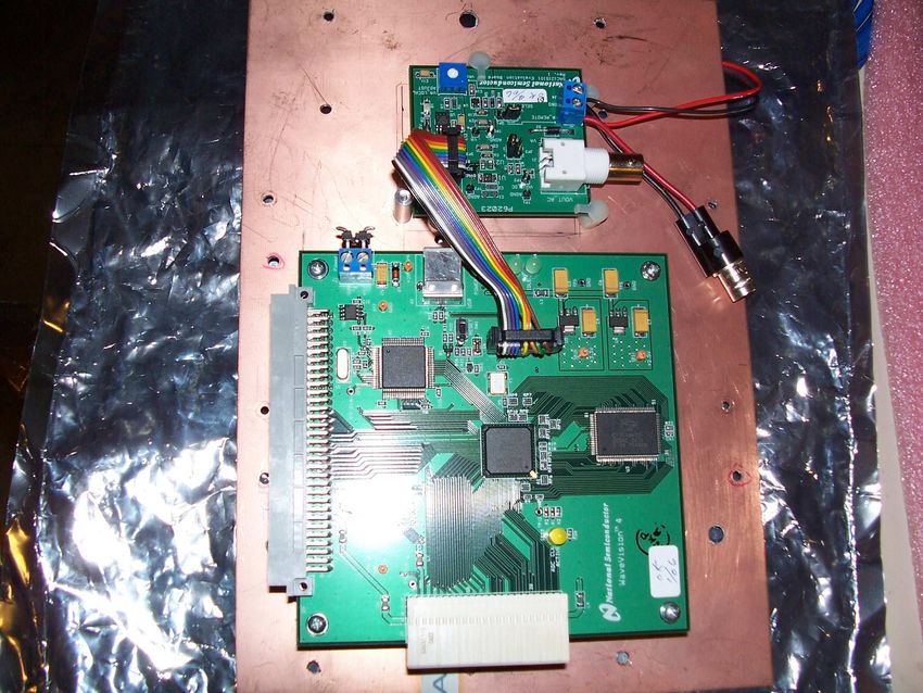
Evalulation and WaveVision 4 boards
Evaluation
board
WaveVision 4
board
Boards were mounted on the Cyclotron Accelerator chamber
8 of 12 Rev. BNational Semiconductor Corporation
2900 Semiconductor Drive +1 408 721 5000 Tel
Santa Clara, CA 95052-8090 USA www.national.com
Appendix A
Heavy-Ion Cocktail Bragg Curves
Fig. A1 is a Bragg curve plot from the Lawrence Berkeley National Laboratory [7] that
shows the depth of penetration and energy for each ion used in the experiment. The
ADC08D1000W-MLS had a thickness of 11 µm from the top of the passivation to the
bottom of the epi layer. From Fig. A1, one can see that at 11 µm, none of the ions start to
lose energy and some have a slight increase in energy. Thus, the LET value of the ion is
almost constant as it passes through the sensitive charge collection region of the transistor.
As a result, the need to correct LET magnitudes used in the report (for penetration depth)
was eliminated.
Fig. A1. LET vs. penetration profile for various ion species used in the heavy-
ion experiments. After [7].
9 of 12 Rev. BNational Semiconductor Corporation
2900 Semiconductor Drive +1 408 721 5000 Tel
Santa Clara, CA 95052-8090 USA www.national.com
Appendix B
4.5 MeV/nucleon cocktail (HeH+1 to Bi)
This cocktail, based on a tune-up of the ion source and Cyclotron using 40Ar+8, has an A/q
ratio of 5 and energy of 4.5 MeV/nucleon. To achieve lower LET, boron can be added by
special request. For even lower LET, HeH+1 ions can be accelerated; this requires a
special tune-up. For an LET of about 100 MeV/mg/cm2, 209Bi+41 can be run at this
energy, but requires advance notice and the AECR-U ion source. All of the above
information was obtained from LBNL.
Table B1. Heavy-ion cocktail used in the SEE experiments.
Ion Energy(MeV) LET (MeV/mg/cm2) # Range in Si (µm) #
HeH+1* 18, 4.5 0.26,0.064 180,179
10
B+2 45 1.64 79
15
N+3 67 3.09 67
20
Ne+4 90 5.77 53
40
Ar+8 180 14.3 48
59
Co+12 266 27.31 43
65
Cu+13 293 29.89 44
78
Kr+15 325 39.54 41
86
Kr+17 378 39.24 47
136
Xe+27 603 68.83 48
209
Bi+41 940 99.64 54
#
LETs and ranges calculated using SRIM2003
*
After break up in target or a scattering foil.
10 of 12 Rev. BTable 1 – Test Log
Date: 06/15/2006
Facility: Lawrence Berkeley National Laboratory
Product Type: ADC14155
DUT’s: ADC14155 evaluation board with DUT #85D (Runs 47 – 60)
Spec Effective Eval Bd Flux ∆ (diff) Applied Temp. Total Accumul-ated
Run ies Incident LET Flux Fluence #events Current Duration Latchup Voltage °C Effective (note 1)
# MeV/ #/cm2* Current Va/Vdr @ Fluence Ionizing
Angle Mg/cm2 sec #/cm2 & type (mA) (sec) mA (V) therm. #/cm2 Dose(rads)
47 Bi209 0° 99.85 3E4 7.07E6 0 455 246 NA 3.3/1.8 35 7.07E6 11.295E3
48 Bi209 0° 99.85 3E4 1.01E7 0 457 298 NA 3.3/1.8 35 1.01E7 27.431E3
49 Bi209 0° 99.85 3E4 1.01E7 0 457 357 NA 3.3/1.8 35 1.01E7 43.567E3
50 Bi209 35° 121.89 5E4 1.01E7 0 457 471 NA 3.3/1.8 35 2.00E7 63.264E3
51 Bi209 35° 121.89 6E4 1.01E7 0 458 520 NA 3.3/1.8 35 2.01E7 82.961E3
52 Bi209 35° 121.89 5E4 1.03E7 0 459 552 NA 3.3/1.8 35 2.02E7 103.049E3
58 Bi209 0° 99.85 4E4 1.00E7 0 478 236 NA 3.3/1.8 65 1.00E7 119.025E3
59 Bi209 0° 99.85 4E4 1.00E7 0 478 233 NA 3.3/1.8 65 1.00E7 135.001E3
60 Bi209 0° 99.85 4E4 1.01E7 0 478 233 NA 3.3/1.8 65 1.01E7 151.137E3
Table 2 – Test Log
Date: 06/16/2006
DUT’s: ADC14155 evaluation board with DUT #84D (Runs 62 – 70)
Spec Effective Eval Bd Flux ∆ (diff) Applied Temp. Total Accumul-ated
Run ies Incident LET Flux Fluence #events Current Duration Latchup Voltage °C Effective (note 1)
# MeV/ #/cm2* Current Va/Vdr @ Fluence Ionizing
Angle Mg/cm2 sec #/cm2 & type (mA) (sec) mA (V) therm. #/cm2 Dose(rads)
62 Bi209 0° 99.85 3E4 1.50E7 0 461 246 NA 3.3/1.8 35 1.50E7 23.964E3
63 Bi209 0° 99.85 3E4 1.01E7 0 462 298 NA 3.3/1.8 35 1.01E7 40.100E3
64 Bi209 0° 99.85 3E4 1.00E7 0 464 357 NA 3.3/1.8 35 1.00E7 56.076E3
65 Bi209 35° 121.89 3E4 1.05E7 0 465 471 NA 3.3/1.8 35 1.27E7 76.553E3
66 Bi209 35° 121.89 2.8E4 1.00E7 0 465 520 NA 3.3/1.8 35 1.22E7 96.056E3
67 Bi209 35° 121.89 2.3E4 1.01E7 0 466 552 NA 3.3/1.8 35 1.23E7 115.753E3
68 Bi209 35° 121.89 2.3E4 1.00E7 0 477 236 NA 3.3/1.8 65 1.20E7 135.256E3
69 Bi209 35° 121.89 2.3E4 1.02E7 0 477 233 NA 3.3/1.8 65 1.25E7 155.148E3
70 Bi209 35° 121.89 2.3E4 1.02E7 0 477 233 NA 3.3/1.8 65 1.24E7 175.040E3
11 of 12 Rev. BTable 3 – Test Log
Date: 06/16/2006
DUT’s: ADC14155 evaluation board with DUT #64C (Runs 71 – 76)
Spec Effective Eval Bd Flux ∆ (diff) Applied Temp. Total Accumul-ated
Run ies Incident LET Flux Fluence #events Current Duration Latchup Voltage °C Effective (note 1)
# MeV/ #/cm2* Current Va/Vdr @ Fluence Ionizing
Angle Mg/cm2 sec #/cm2 & type (mA) (sec) mA (V) therm. #/cm2 Dose(rads)
71 Bi209 35° 121.89 3.0E5 1.20E7 0 462 55 NA 3.3/1.8 35 1.50E7 23.403E3
72 Bi209 35° 121.89 3.0E5 1.01E7 0 464 44 NA 3.3/1.8 35 1.20E7 43.100E3
72 Bi209 35° 121.89 2.7E5 1.05E7 0 464 46 NA 3.3/1.8 35 1.30E7 63.578E3
74 Bi209 35° 121.89 2.5E5 1.03E7 0 477 44 NA 3.3/1.8 65 1.26E7 83.665E3
75 Bi209 35° 121.89 3.0E5 1.04E7 0 477 45 NA 3.3/1.8 65 1.26E7 103.948E3
76 Bi209 35° 121.89 3.0E5 1.02E7 0 477 44 NA 3.3/1.8 65 1.25E7 123.840E3
Note 1: Accumulated Ionizing Dose is an estimate of the worst case bound according to annex B of EIA/JESD57. The large Z (number of protons) species
used in this testing lose their energy and stop rather quickly in Si (although the depth vs. LET curve of all the species used showed that the rapid drop off of
LET and the penetration depth was well below the epitaxial layer and into the substrate, that is well below the active circuitry and associated parasitics). The
formula given in annex B of EIA/JESD57, 1.6E-5*LET*Fluence, with LET in MeV/mg/cm2, and Fluence in ions/cm2, assumes that the LET of the species
does not decrease and the ion flux continues on through the Si undiminished. Thus, the accumulated ionizing dose presented in the last two tables is certainly
an over estimate, and the over estimate gets worse with as Z gets larger. Certainly for Bi209, these figures are greatly over estimated. Through out the testing
the performance of the DUT’s with checked with WaveVision4 software (developed by National Semiconductor Corp.) and no degradation of performance
was observed on any of the DUT’s.
12 of 12 Rev. BIMPORTANT NOTICE
Texas Instruments Incorporated and its subsidiaries (TI) reserve the right to make corrections, modifications, enhancements, improvements,
and other changes to its products and services at any time and to discontinue any product or service without notice. Customers should
obtain the latest relevant information before placing orders and should verify that such information is current and complete. All products are
sold subject to TI’s terms and conditions of sale supplied at the time of order acknowledgment.
TI warrants performance of its hardware products to the specifications applicable at the time of sale in accordance with TI’s standard
warranty. Testing and other quality control techniques are used to the extent TI deems necessary to support this warranty. Except where
mandated by government requirements, testing of all parameters of each product is not necessarily performed.
TI assumes no liability for applications assistance or customer product design. Customers are responsible for their products and
applications using TI components. To minimize the risks associated with customer products and applications, customers should provide
adequate design and operating safeguards.
TI does not warrant or represent that any license, either express or implied, is granted under any TI patent right, copyright, mask work right,
or other TI intellectual property right relating to any combination, machine, or process in which TI products or services are used. Information
published by TI regarding third-party products or services does not constitute a license from TI to use such products or services or a
warranty or endorsement thereof. Use of such information may require a license from a third party under the patents or other intellectual
property of the third party, or a license from TI under the patents or other intellectual property of TI.
Reproduction of TI information in TI data books or data sheets is permissible only if reproduction is without alteration and is accompanied
by all associated warranties, conditions, limitations, and notices. Reproduction of this information with alteration is an unfair and deceptive
business practice. TI is not responsible or liable for such altered documentation. Information of third parties may be subject to additional
restrictions.
Resale of TI products or services with statements different from or beyond the parameters stated by TI for that product or service voids all
express and any implied warranties for the associated TI product or service and is an unfair and deceptive business practice. TI is not
responsible or liable for any such statements.
TI products are not authorized for use in safety-critical applications (such as life support) where a failure of the TI product would reasonably
be expected to cause severe personal injury or death, unless officers of the parties have executed an agreement specifically governing
such use. Buyers represent that they have all necessary expertise in the safety and regulatory ramifications of their applications, and
acknowledge and agree that they are solely responsible for all legal, regulatory and safety-related requirements concerning their products
and any use of TI products in such safety-critical applications, notwithstanding any applications-related information or support that may be
provided by TI. Further, Buyers must fully indemnify TI and its representatives against any damages arising out of the use of TI products in
such safety-critical applications.
TI products are neither designed nor intended for use in military/aerospace applications or environments unless the TI products are
specifically designated by TI as military-grade or "enhanced plastic." Only products designated by TI as military-grade meet military
specifications. Buyers acknowledge and agree that any such use of TI products which TI has not designated as military-grade is solely at
the Buyer's risk, and that they are solely responsible for compliance with all legal and regulatory requirements in connection with such use.
TI products are neither designed nor intended for use in automotive applications or environments unless the specific TI products are
designated by TI as compliant with ISO/TS 16949 requirements. Buyers acknowledge and agree that, if they use any non-designated
products in automotive applications, TI will not be responsible for any failure to meet such requirements.
Following are URLs where you can obtain information on other Texas Instruments products and application solutions:
Products Applications
Audio www.ti.com/audio Automotive and Transportation www.ti.com/automotive
Amplifiers amplifier.ti.com Communications and Telecom www.ti.com/communications
Data Converters dataconverter.ti.com Computers and Peripherals www.ti.com/computers
DLP® Products www.dlp.com Consumer Electronics www.ti.com/consumer-apps
DSP dsp.ti.com Energy and Lighting www.ti.com/energy
Clocks and Timers www.ti.com/clocks Industrial www.ti.com/industrial
Interface interface.ti.com Medical www.ti.com/medical
Logic logic.ti.com Security www.ti.com/security
Power Mgmt power.ti.com Space, Avionics and Defense www.ti.com/space-avionics-defense
Microcontrollers microcontroller.ti.com Video and Imaging www.ti.com/video
RFID www.ti-rfid.com
OMAP Mobile Processors www.ti.com/omap
Wireless Connectivity www.ti.com/wirelessconnectivity
TI E2E Community Home Page e2e.ti.com
Mailing Address: Texas Instruments, Post Office Box 655303, Dallas, Texas 75265
Copyright © 2012, Texas Instruments IncorporatedYou can also read