Silicon subwavelength grating waveguides with high-index chalcogenide glass cladding
←
→
Page content transcription
If your browser does not render page correctly, please read the page content below
Silicon subwavelength grating waveguides with
high-index chalcogenide glass cladding
Philippe Jean, Alexandre Douaud, Sophie LaRochelle, Younès Messaddeq, and Wei
Shi

OSA Optics Express, (Vol. 29, No. 13) (21 June 2021)

https://doi.org/10.1364/OE.430204

© 2021 Optical Society of America under the terms of the OSA Open Access
Publishing Agreement.
Research Article                                      Vol. 29, No. 13 / 21 June 2021 / Optics Express 20851

Silicon subwavelength grating waveguides with
high-index chalcogenide glass cladding
P HILIPPE J EAN , 1,2 A LEXANDRE D OUAUD , 1 S OPHIE
L A R OCHELLE , 1,2 YOUNÈS M ESSADDEQ , 1,3 AND W EI S HI 1,2,*
1 Centred’Optique, Photonique et Laser (COPL), 2375 rue de la Terrasse, Université Laval, Québec G1V
0A6, Canada
2 Département de Génie Électrique et de Génie Informatique, Université Laval, 2325, rue de l’Université,
Québec G1V 0A6, Canada
3 Département de Physique, de Génie Physique et d’Optique, Université Laval, 2325, rue de l’Université,
Québec G1V 0A6, Canada
* wei.shi@gel.ulaval.ca

Abstract: Silicon subwavelength grating waveguides enable flexible design in integrated
photonics through nano-scale refractive index engineering. Here, we explore the possibility of
combining silicon subwavelength gratings waveguides with a high-index chalcogenide glass as
a top cladding, thus modifying the waveguiding behavior and opening a new design axis for
these structures. A detailed investigation of the heterogeneous SWG waveguide with high-index
cladding is presented based on analytical and numerical simulations. We design, fabricate and
characterize silicon subwavelength grating waveguide microring resonators with an As20 S80
cladding. Thanks to As20 S80 negative thermo-optic coefficient, we achieve near athermal behavior
with a measured minimum thermally induced resonance shift of −1.54 pm/K, highlighting the
potential of subwavelength grating waveguides for modal confinement engineering and to control
light-matter interaction. We also show that the chalcogenide glass can be thermally reflowed to
remove air gaps inside the cladding, resulting in a highly conformal structure. These types of
waveguides can find application in reconfigurable photonics, nonlinear optics, metamaterials or
slow light.

© 2021 Optical Society of America under the terms of the OSA Open Access Publishing Agreement

1.    Introduction
Advances in fabrication technology have put forward the potential of controlling light at the
subwavelength scale in order to boost the performance and flexibility of integrated optic
components. To this end, silicon subwavelength grating waveguides (SWGs) are a prominent
example of subwavelength engineering that led to substantial performance improvements in
practical applications [1]. SWGs are one-dimensional periodic waveguides with feature size
that are much smaller than their operating wavelengths, such that the relation λ>>2neff Λ
approximately holds [2]. As such, they support the diffraction-less propagation of a Bloch mode,
whose properties can be controlled through not only careful design of their cross-sections but
also by controlling the period Λ and the duty-cycle DC = LSi /Λ.
   The added degrees of freedom of SWG provide more flexibility in their design; in the deep
subwavelength limit, light sees the grating as an homogeneous material with a weighted refractive
index, thus opening the possibility of refractive index engineering [3]. Index engineering can
be used to multiple ends. A few key examples include on-chip control of group delay [4,5],
bandwidth increase of contra-directional couplers [6] or of multimode interferometers [7], on-chip
polarization management [7–9], polarization-independent and efficient fiber-to-chip edge couplers
[10,11] and engineering of the bandwidth of Bragg filters [12].
   In addition to index engineering, SWGs are also interesting to control light-matter interaction
with the waveguide top cladding, which can be air or an analyte for sensing [13,14], a material

#430204                                                                      https://doi.org/10.1364/OE.430204
Journal © 2021            Received 28 Apr 2021; revised 2 Jun 2021; accepted 9 Jun 2021; published 17 Jun 2021
Research Article                                       Vol. 29, No. 13 / 21 June 2021 / Optics Express 20852

with a negative thermo-optic coefficient TOC for thermal compensation [15] or even a potential
rare-earth ions host for amplification [16]. The use of exotic cladding materials is therefore a
promising emergent topic with potential to add another degree of freedom in designing SWGs.
Among the materials that are amenable for heterogeneous integration with SWG, chalcogenide
glasses (ChG) present a set of unique and attractive properties for photonics, including low-loss
over a large transparency window, photosensitivity, high non-linearity and a high refractive index
[17]. Chalcogenides are also excellent materials for the important field of Brillouin photonics as
their low density allow for acoustic waveguiding in addition to optical waveguiding [18]. The
development of hybrid chalcogenide-silicon waveguides is a promising approach to harness
interesting chalcogenide properties on the silicon platform [19,20].
   In this work, we study the combination of silicon SWGs with a high-index chalcogenide
glass top cladding. The effect of using a high-index material is first explored through analytical
methods. A novel As20 S80 -on-Si SWG design is demonstrated using the finite-difference time
domain (FDTD) method. Next, microring resonators (MR) based on the designed waveguide are
fabricated. The passive optical properties and thermal response of the fabricated MR are measured
at telecommunication wavelengths. The MR exhibit intrinsic quality factor of Q = 5.6 × 10⁴
and athermal behavior with a slightly negative wavelength shift of ∆λr /∆T = −1.54 pm/K. We
also demonstrate that the use of a chalcogenide soft glass can eliminate the formation of air gaps
inside the cladding.

2.     SWG with high-index claddings
2.1.    1D analytical model
In contrast with conventional 2D waveguides (e.g. strips or ribs), SWGs support the propagation
of a Bloch mode with properties that are affected by the periodic nature of the waveguide
permittivity. Therefore, 2D simulation methods like finite difference eigenmode (FDE) cannot
fully capture the intricacy of SWGs optical properties. Rigorous 3D simulation methods like
finite-difference time domain (FDTD) can be used to accurately predict the waveguides behavior,
but they are computationally expensive and time consuming. Insight into the Bloch mode behavior
and initial design guidelines can be obtained by realizing that the peculiarities of the SWGs are
akin to the propagation of a plane wave inside a periodic dielectric stack that is semi-infinite in
the transversal directions, hereafter referred to as a Bragg stack (BS). The basic features of Bloch
mode propagation can then be modelled using an analytical 1D approach. A BS with alternating
material permittivities ϵ1 = n21 and ϵ2 = n22 and period Λ is schematically shown in the inset (i) of
Fig. 1(a). At normal incidence, the dispersion relation of a BS is given as [21,22]

                                                            (n21 + n22 )
                   cos (KΛ) = cos (k1 l1 ) cos (k2 l2 ) −                sin (k1 l1 ) sin (k2 l2 ),             (1)
                                                             (2n1 n2 )
                                                                       2πn
where K is the Bloch mode propagation constant and k1,2 = λ1,2 is the wavenumber. The length
of each material is given as l1 + l2 = Λ and the duty-cycle, or filling factor, is DC = l1 /Λ. For
the specific case of this work, ϵ is considered real as the materials absorption are neglected, but
we note that they can be included by simply considering an imaginary part to ϵ [22]. The relation
of Eq. (1) is limited in two ways: (1) it ignores the effect of transversal confinement, which is
substantial in high-index contrast waveguides and (2) it considers a crystal that extends to infinity
along the propagation axis. The first limitation can be easily solved by using 3D methods, as
previously mentioned. The finite nature of real devices, on the other hand, requires careful design
of the tapers to efficiently inject into Bloch modes from standard waveguide modes [23,24].
Nevertheless, such a simplified model can provide insight into the behavior of SWG at negligible
computational cost and serve as an initial design tool.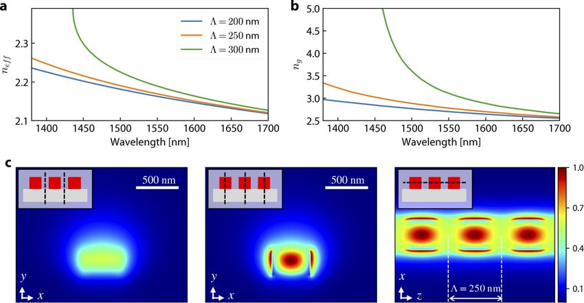
Research Article                                        Vol. 29, No. 13 / 21 June 2021 / Optics Express 20853

       Fig. 1. Propagation of the Bloch mode in a dielectric stack. (a) Bandstructure simulated
       using the analytical model of Eq. (1) (solid line) and using a metamaterial approximation
       (dashed line) with a fixed index contrast ∆n = 0.5. Inset (i): 1D geometry of the BS. Inset
       (ii): Close-up view near the bandgap showing the deviation between the model of Eq. (1)
       and the metamaterial approximation (see text). (b) Map of the Bloch mode normalized
       propagation constant for varying refractive index contrast between the stacks. The vertical
       dashed line indicates the geometry for which the bandstructure is shown in (a) and the black
       solid lines delimit the extent of the bandgap. (c) Band-edge location in an infinite crystal with
       different minimum periods. The minimum feature size for DC = 0.5 is half the period Λ/2.
       The red shaded regions highlight commonly used spectral bands in telecommunications. (d)
       Engineering the effective index by tuning the material index and the waveguide duty-cycle
       DC. The normalized wavelength is fixed at λ/Λ = 7.75.

   The effect of high-index cladding is first explored using Eq. (1) by setting n2 as the cladding
material refractive index with a constant n1 = 2.5 to represent the index of the silicon period,
close to the effective index of a 500 nm wide silicon nanowire at 1550 nm. The effect of index
contrast ∆n = |n1 − n2 | on the propagation properties is summarized in Fig. 1(a) through (d).
The bandstructure near the first order bandgap of a BS with ∆n = 0.5 and DC = 0.5 is shown
in Fig. 1(a). The result obtained from Eq. (1) is compared with a metamaterial approximation
n2meta = Λ−1 (l1 ϵ1 + l2 ϵ2 ). As expected, the BS propagation constant K tends toward that using the
metamaterial in the deep-subwavelength λ>>Λ but deviates significantly when approaching the
bandgap.
   The main effect of reducing the index contrast is the narrowing of the bandgap, as seen in
Fig. 1(b), which is expected as the BS approaches a uniform medium in the limit ∆n → 0. This
narrowing is accompanied by a shift of the band-edges λBE , the blue- and red-side wavelength
boundaries of the bandgap, which effectively limits the operation in the deep-subwavelength
regime at a given wavelength. This is important considering that the minimum feature size of
electron-beam lithography and UV photolithography are about 60 nm and 150 nm, respectively.
The fabrication minimum feature size then puts a hard limit on how far away from the bandgap
the waveguide can be designed to operate. It is well known that silicon SWG do not really
operate in the deep-subwavelength regime, where they could be treated using an effective medium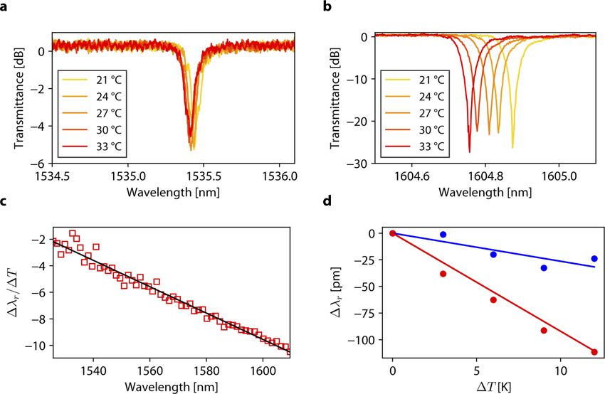
Research Article                                  Vol. 29, No. 13 / 21 June 2021 / Optics Express 20854

theory, but are effectively operating in the transition region [1]. In Fig. 1(c), the position of the
red-side band-edge λBE is plotted for various Λ and refractive index contrast ∆n. With DC = 0.5,
the minimum feature size required is half the period Λ/2. It is clear that one must be careful
when using high-index materials with SWGs as the band-edge creeps rapidly towards common
operating wavelengths in the O-band or C-band, for example. We also note that proximity to
the band-edge is to be carefully considered, as even if the light is not diffracted in the bandgap,
multiple scattering, slow light and Bloch mode reshaping can drastically increase the propagation
losses [5,25]. The extent to which the effective index of a BS operating in the SWG regime
(λ/Λ = 7.75) can be engineering is shown in Fig. 1(d). A large span of effective index can be
achieved by tuning the SWG duty-cycle and using cladding materials with different refractive
index.
   The analytical model of Eq. (1) is then used to study the effect of high-index cladding on
the optical field distribution inside the BS. We use the dimensionless confinement factor Γi ,
describing the interaction between the Bloch mode and material i such as [26,27]

                                             ng i ϵ |E| 2 dV
                                                ∫
                                       Γi =                  ,                                    (2)
                                              ni ϵ |E| 2 dV
                                                ∫

where ng is the group index, ni is the material for which Γi is considered, ϵ is the dielectric
permittivity and E is the vectorial electric field. The integral in Eq. (2) is taken over the volume V
of a single unit-cell. For the BS, the integral reduce to a single dimension. We note that Γi really
consider two distinct effects, the slow light enhancement and the energy density distribution.
While the second takes value between 0 and 1, the slow light enhancement results in Γ>1 near
the bandgap [26].
   The normalized wavelength dependence of Γ is presented using an analogue to the bandstructure
in Fig. 2(a), with the different operation regions identified for clarity. In the deep-subwavelength
limit, the confinement factor is directly proportional to the material index and to the duty-cycle,
indicating a uniform distribution of the field over the unit cell or, in other words, that the
periodicity does not affect the mode distribution. The effect of periodicity becomes significant in
the transition region, where ΓSi increases until it diverges at the band-edge. This is associated
with a reshaping of the Bloch mode and increased(decreased) interaction with the high(low)-index
material. This behavior of enhanced light-matter interaction near the band-edge of photonic
crystals is responsible for a variety of interesting effects, including gain enhancement for lasers
[28] or the optical Borrmman effect [29]. Fig. 2(b) shows the normalized electric field intensity
inside along the propagation axis of one unit cell for various parameters, highlighting the mode
redistribution into the high index period due to both the wavelength dependence (left panel) and
the index contrast (right panel). The sharp increase of ΓSi and associated decrease of Γclad in the
transition region have consequences in applications where the SWG is used to enhance interaction
with the cladding material, such as in thermal compensation [15]. The effect of thermally induced
perturbations are important for integrated optics in general and relevant in the context of ChG
functionalization [30–32]. Using the confinement factors, the effective thermo-optic coefficient
TOCeff = dneff /dT can be calculated to a first-order approximation as [32]

                                      dneff      dn1      dn2
                                            ≈ Γ1     + Γ2     .                                          (3)
                                       dT        dT       dT
  In this work, we consider the case where n1 is silicon and has a thermo-optic coefficient of
dnSi/1 /dT = 1.8 × 10⁻⁴ RIU/K [33] while the material n2 is As20 S80 , with n2 = nAs20 S80 = 2.15
and dnChG/2 /dT = −5 × 10⁻⁵ [31].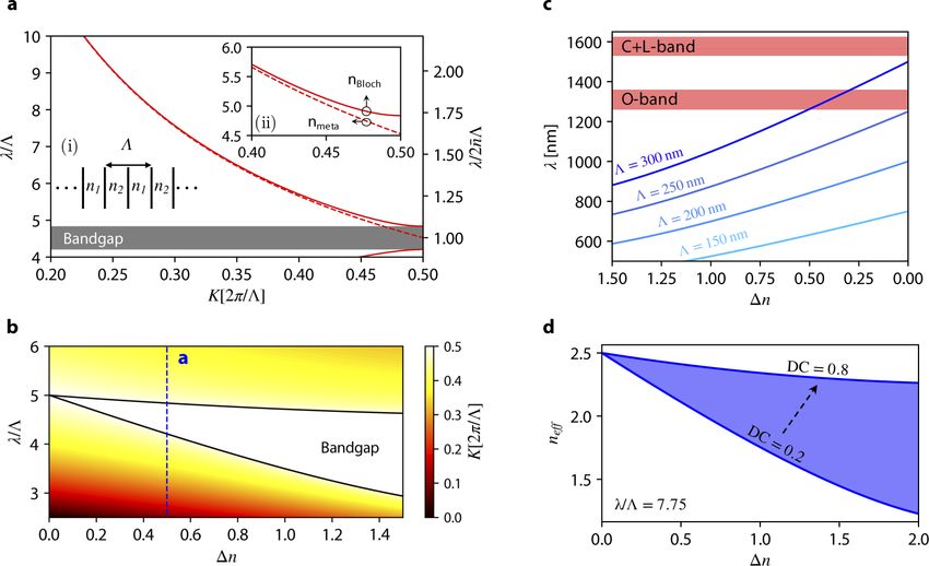
Research Article                                     Vol. 29, No. 13 / 21 June 2021 / Optics Express 20855

        Fig. 2. Confinement factor of the Bloch mode in a dielectric stack simulated using the model
        of Eq. (1). (a) Confinement factor in the silicon (red solid line) and in the glass (solid blue
        line) as a function of normalized wavelength λ/Λ with a fixed ∆n = 0.5. The vertical dashed
        lines serve to approximately delimit the operation regions (SWG, transition and band-edge).
        The bandgap is indicated as the dark grey area. Inset: Confinement factor ratio Γclad /ΓSi
        that tends towards n2 /n1 in the SWG limit (dashed line). (b) Normalized electric field
        intensity along one period (top) for various normalized wavelengths λ/Λ = [4.85, 5, 6, 10]
        and fixed ∆n = 0.5 and (bottom) for various index contrast ∆n = [0.7, 0.5, 0.3, 0.1] and fixed
        λ/Λ = 7.75.

2.2.    FDTD simulations
Following the basic design guidelines provided by the analytical simulations of the previous
section, we simulated an SWG with a 800 nm As20 S80 cladding, which is expected to provide
thermal compensation while allowing to operate sufficiently far away from the band-edge to
avoid detrimental effects. The periodicity in the FDTD simulation was achieved using Bloch
boundary conditions along the propagation axis and the simulation time window was 2000 fs
(time step of 0.02 fs). The simulation window is 16 µm wide and 8 µm high and the meshing is
set to 10 nm in all direcitons around the silicon block. The simulated waveguide parameters are
w = 450 nm, t = 220 nm and DC = 0.5. Three periods are considered: Λ = [200, 250, 300] nm.
   The effective index and group index of the heterogeneous SWG are shown in Fig. 3(a) and (b),
respectively. We observe the absence of bandgap related distortion down to at least λ = 1400
nm for Λ = 200 nm, so that the SWG is expected to operate in the transition region. The SWG
with Λ = 250 nm shows a moderate increase of ng at shorter wavelength, indicating operation
in the transition region that approaches the bandgap while the SWG with Λ = 300 nm has its
bandgap just short of λ = 1500 nm. The position of the bandgap is represented as a divergence of
the effective and group indices in the plots. The 3D distribution of the electric field intensity at
λ = 1550 nm for Λ = 250 nm is shown in Fig. 3(c). The relatively narrow waveguide geometry
and reduced effective refractive index results in a delocalization of the mode outside of the silicon
block in the transversal directions. The right panel of Fig. 3(c) shows a top view where the
concentration of |E| 2 inside the silicon is clearly visible, indicating that the SWG does not operate
in the deep-subwavelength region. The confinement factors are ΓSi = 0.28, Γclad = 0.89 and
                                                                                     dn
ΓSiO2 = 0.06. The thermo-optic coefficient of the waveguide is predicted to be dTeff = 6.3 × 10⁻⁶
using the material thermo-optic coefficient (TOC) reported in Ref. [31]. This corresponds to
Research Article Vol. 29, No. 13 / 21 June 2021 / Optics Express 20856
a resonant wavelength shift of ∆λr /∆T = 6.2 pm/K in a microring resonator with R = 100 µm.
We note that the large ratio of Γclad /ΓSi >3 in TE polarization is a good example of the SWG
advantage in increasing light-matter interaction with top cladding materials.
Fig. 3. (a) and (b) Effective index and group index simulated using 3D-FDTD for an
As20 S80 clad SWG with w = 450 nm, DC = 0.5 and different periods(b) Electric field
intensity distribution of the Bloch mode for Λ = 250 nm in the (left) xy plane in the glass,
(center) xy plane in the Si and (right) zx plane at mid-height in the waveguide for 3 periods.
3. Fabrication
Next, the waveguide simulated using FDTD in the last section was used to design and fabricate
microring resonators. MRs were chosen instead of straight waveguides because they provide
measurement of the group index, propagation loss and thermo-optic coefficient in a very compact
footprint. In addition, estimating the waveguide loss from the MRs response instead of using
the cutback methods alleviates the error arising from variations in the fiber-to-chip coupling
when depositing the cladding on individual chips. The silicon chips were processed using
electron-beam lithography by Applied NanoTools through the SiEPICfab consortium [34] on
220 nm thick silicon-on-insulator wafers with 2 µm thick buried oxide (BOx) layer. The glassy
thin-films were deposited in-house using the same method as described in Ref. [31], including
the 120 s annealing step at T = 150 ◦ C. The measured deposited cladding thickness is 890 nm. A
schematic of the heterogeneous SWG is provided in Fig. 4(a). Scanning electron microscope
(SEM) images were taken before the glass deposition. A top view SEM image of an MR is shown
in Fig. 4(b) with the inset showing a close-up of the coupling region between the ring and the bus
waveguide. The routing strip waveguides (500 nm × 220 nm) were converted into SWGs using
linear geometrical tapers of length Ltaper = 100 µm, similar to those used in [5]. The fabricated
device had a radius R = 100 µm, a width w = 450 nm, a period Λ = 250 nm and a duty-cycle
DC = 0.5.
A common difficulty when fabricating oxide-clad silicon devices with tiny features like SWGs
is the formation of air voids that are not filled by the oxide [35]. These voids can lead to
significant performance deviation from the intended design. The use of materials that can be
reflowed at low temperature, like chalcogenides, can suppress these gaps and lead to a conformal
structure where the cladding material completely covers the silicon. This effect in the As20 S80
cladded SWGs was investigated using focused ion beam milling (FIB) to image the waveguideResearch Article Vol. 29, No. 13 / 21 June 2021 / Optics Express 20857
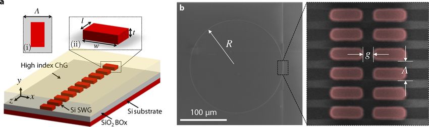
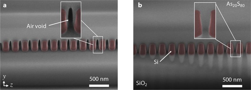
Fig. 4. Silicon SWG waveguides and microresonators with high-index ChG cladding. (a)
Schematic drawing of an SWG waveguide with period Λ, width w. Inset (i): Top view of a
single unit cell. Inset (ii): Geometry of a single silicon block. (b) Top view SEM image of a
fabricated SWG microresonator of radius R with a close-up view of the coupling as inset
(right).
along its propagation axis in a sample before annealing (as-deposited) and in a sample after
thermal annealing. The as-deposited sample had systematic voids, as visible in Fig. 5(a), where
the air appears as darker patterns. Thermal annealing resulted in the reflow of the glass and a
complete filling between the silicon blocks, as visible in Fig. 5(b). We note that this aggressive
reflow at moderate temperature (T = 150◦ C) is possible due to the quasi-polymeric behavior
of the sulfur-rich chalcogenide composition [36]. A similar effect was reported in silicon slot
waveguides covered with As2 S3 for nonlinear photonics [20].
Fig. 5. SEM images of fabricated heterogeneous SWG waveguides with FIB cut along the
propagation axis before (a) and after (b) thermal annealing. The insets show close-up views
of the glass between the silicon pillars, showing the air gap before annealing and the filling
of the gap by the glass after annealing.
4. Optical characterization
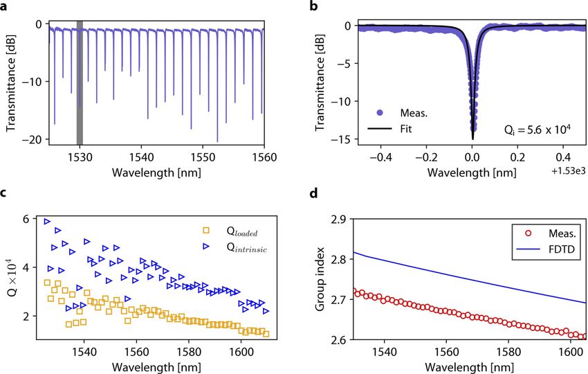
4.1. Passive response
The optical response of an SWG MR with g = 300 nm was measured using an optical vector
analyzer (OVA5000 from LUNA). The chip stage was mounted on a Peltier module with a
temperature controller (TEC) to stabilize the operation at T = 20 ◦ C. The results are summarized
in Fig. 6(a) through (d).
The transmittance is shown in Fig. 6(a) while a single resonance is identified and zoomed
on in (b). From the resonances, the group index can be calculated and is presented in Fig. 6(d)
alongside simulated values using 3D-FDTD. We note that the linear increase of group index
with frequency suggests the absence of band-edge proximity effect and operation away fromResearch Article Vol. 29, No. 13 / 21 June 2021 / Optics Express 20858
Fig. 6. Passive optical characterization of an As20 S80 clad SWG microring resonator with
Λ = 250 nm, DC = 0.5, w = 450 nm and g = 300 nm. (a) Normalized transmittance in the
C-band. (b) Single resonance with Qi = 5.6 × 10⁴ near 1530 nm (identified as the shaded
region in (a)). (c) Quality factors measurement over the C+L band. (d) Measured (red
markers) and simulated (blue line) group index over the C+L band.
the bandgap, as expected from the FDTD simulations. The difference between the simulated
and measured values of group index could arise from a variety of fabrication errors that are
non-trivial to separate. We also mention that the dispersion of As20 S80 used in the simulations
was obtained using a prism-coupling method with a certain degree of uncertainty, which could
explain the difference [31]. Next, the waveguiding loss is assessed through the MR quality
factor Q = λ/FWHM, calculated using a Lorentzian fit on each resonance, as in Fig. 6(b). The
wavelength dependence of the loaded and intrinsic Q is shown in 6(c). The intrinsic quality-factor
Qi and the associated propagation loss α are calculated using the formulas [37,38]
2Q 2πng
Qi = √ ≈ , (4)
1 + T0 αλres
where T0 is the normalized transmittance at the resonant wavelength. Eq. (4) assumes undercou-
pled operation, which is the case for the device considered in this work. Leakage to the substrate
is not expected in this geometry due to the mode displacement in the ChG cladding and associated
high effective index [16,39]. The reduction of loss at shorter wavelength reinforces the idea
that the SWG operates sufficiently far from the band-edge. The highest intrinsic quality-factor
measured is Qi = 5.6 × 10⁴ and corresponds to waveguide propagation loss of around α = 8.6
dB/cm. The propagation losses are comparable to those recently reported in tellurium dioxide
clad SWG [16]. We note that the SWG presented here was specifically designed to operate in TE
polarization. The TM polarization in this structure is strongly delocalized and large bending
losses are expected even for R = 100 µm. Because of this, the TM response of the MR was not
observed in the measurements.
4.2. Thermal response
Finally, the thermal response of the heterogeneous SWG was investigated by increasing the TEC
temperature in steps of 3 ◦ C and monitoring the MR resonant wavelength shift. The results areResearch Article Vol. 29, No. 13 / 21 June 2021 / Optics Express 20859
summarized in Fig. 7(a) through (d), where (a) and (b) are examples of measurement of two
resonances: one at shorter wavelength with a nearly temperature independent behavior and one
at longer wavelength with a strong negative dependence, respectively.
Fig. 7. Thermal measurements of a As20 S80 clad SWG with Λ = 250 nm, DC = 0.5 and
w = 450 nm. (a,b) Normalized transmittance of a single resonance with a low (a) and high
(b) thermo-optic coefficient. (c) Temeperature dependent resonance shift coefficient ∆λr /∆T
measured over the C+L band. Linear fits used to extract ∆λr /∆T from the resonances shown
in blue (a) and red (b).
The resonance shift ∆λr is extracted for each measured trace and a linear fit is used to extract the
resonance shift coefficient ∆λr /∆T. Two examples of this process are shown in Fig. 7(d) while the
full wavelength dependent data is shown in Fig. 7(c). ∆λr /∆T decreases at longer wavelength as
the confinement factor with the negative TOC As20 S80 increases. Thermal compensation between
the silicon positive TOC and ChG negative TOC is nearly perfect at shorter wavelengths. The
minimum value measured is ∆λr /∆T = −1.54 pm/K, indicating that the hybrid MR is virtually
athermal at this wavelength. The value of ∆λr /∆T is slightly lower than the one predicted in
Sect.2. using FDTD simulation. This discrepancy could arise from difference between the
simulated and fabricated SWG, similar to the effect on group index noted in sect.4.1. We also
note that the deposited cladding was slightly thicker than in the simulation (by 90 nm) thus
slightly increasing the overlap with the chalcogenide. We note that the athermal wavelength
could be shifted, resulting in a zero crossing of ∆λr /∆T, by slightly adjusting the geometry of
the waveguide. Increasing the feature size of the silicon will reduce Γclad and shift the curve
in Fig. 7(c) upwards. It is also interesting to calculate the effective thermo-optic coefficient of
waveguide TOCeff = dneff /dT, which can be obtained from measurements using the expression
[40,41] (︄ )︄
dλr λr dneff
= neff αsub + , (5)
dT ng dT
where we assumed that the thermal expansion is governed by the silicon substrate expansion
coefficient αsub = 2.6 × 10⁻⁶ . The effective index is taken from simulation while the other values
are from measurements. Using Eq. (5), the minimum effective TOC is −2.93 × 10⁻⁶ RIU/K. This
value further confirms the extremely low thermal dependence achieved in the hybrid SWG. ThisResearch Article Vol. 29, No. 13 / 21 June 2021 / Optics Express 20860
demonstration of nearly perfect athermality is exemplary of the flexibility of SWG in engineering
light-matter interactions. As such, SWGs are excellent candidates for hybrid integration, where
the properties of exotic materials are used to enhance silicon photonics. It is also important
to emphasize that the use of the hybrid chalcogenide-silicon SWG proposed in this work goes
beyond thermal compensation and could find application in various important fields including
Brillouin photonics [19], amplifiers [42] or reconfigurable photonics [43].
5. Conclusion
In summary, we demonstrated a novel heterogeneous silicon subwavelength grating waveguide
with a high-index chalcogenide glass cladding that exhibits athermal operation and propagation
loss of 8.6 dB/cm. Further work will focus on using the athermal SWG in concrete applications
and improve the loss performance. This work demonstrates the potential of heterogeneous
SWGs to engineer light-matter interaction for some of the most critical challenges facing silicon
photonics.
Funding. Natural Sciences and Engineering Research Council of Canada (STPGP 494358-16); Canada First Research
Excellence Fund (Sentinel North).
Acknowledgments. The authors would like to thank Stéphan Gagnon and Wagner Correr for the SEM/FIB images.
Disclosures. The authors declare no conflicts of interest.
Data availability. Data underlying the results presented in this paper are not publicly available at this time but maybe
obtained from the authors upon reasonable request.
References
1. P. Cheben, R. Halir, J. H. Schmid, H. A. Atwater, and D. R. Smith, “Subwavelength integrated photonics,” Nature
560(7720), 565–572 (2018).
2. P. J. Bock, P. Cheben, J. H. Schmid, J. Lapointe, A. Delâge, S. Janz, G. C. Aers, D.-X. Xu, A. Densmore, and T. J.
Hall, “Subwavelength grating periodic structures in silicon-on-insulator: a new type of microphotonic waveguide,”
Opt. Express 18(19), 20251–20262 (2010).
3. P. Cheben, P. J. Bock, J. H. Schmid, J. Lapointe, S. Janz, D.-X. Xu, A. Densmore, A. Delâge, B. Lamontagne, and T.
J. Hall, “Refractive index engineering with subwavelength gratings for efficient microphotonic couplers and planar
waveguide multiplexers,” Opt. Lett. 35(15), 2526–2528 (2010).
4. Y. Wang, H. Sun, M. Khalil, W. Dong, I. Gasulla, J. Capmany, and L. R. Chen, “On-chip optical true time delay lines
based on subwavelength grating waveguides,” Opt. Lett. 46(6), 1405–1408 (2021).
5. P. Jean, A. Gervais, S. LaRochelle, and W. Shi, “Slow light in subwavelength grating waveguides,” IEEE J. Sel. Top.
Quantum Electron. 26(2), 1–8 (2020).
6. D. Charron, J. St-Yves, O. Jafari, S. LaRochelle, and W. Shi, “Subwavelength-grating contradirectional couplers for
large stopband filters,” Opt. Lett. 43(4), 895–898 (2018).
7. R. Halir, P. Cheben, J. M. Luque-González, J. D. Sarmiento-Merenguel, J. H. Schmid, G. Waguemert-Pérez, D.-X.
Xu, S. Wang, A. Ortega-Monux, and I. Molina-Fernandez, “Ultra-broadband nanophotonic beamsplitter using an
anisotropic sub-wavelength metamaterial,” Laser Photonics Rev. 10(6), 1039–1046 (2016).
8. J. M. Luque-Gonzalez, A. Herrero-Bermello, A. Ortega-Monux, I. Molina-Fernandez, A. V. Velasco, P. Cheben, J. H.
Schmid, S. Wang, and R. Halir, “Tilted subwavelength gratings: controlling anisotropy in metamaterial nanophotonic
waveguides,” Opt. Lett. 43(19), 4691–4694 (2018).
9. X. Guan, P. Chen, S. Chen, P. Xu, Y. Shi, and D. Dai, “Low-loss ultracompact transverse-magnetic-pass polarizer
with a silicon subwavelength grating waveguide,” Opt. Lett. 39(15), 4514–4517 (2014).
10. P. Cheben, J. H. Schmid, S. Wang, D.-X. Xu, M. Vachon, S. Janz, J. Lapointe, Y. Painchaud, and M.-J. Picard,
“Broadband polarization independent nanophotonic coupler for silicon waveguides with ultra-high efficiency,” Opt.
Express 23(17), 22553–22563 (2015).
11. T. Barwicz, Y. Taira, T. W. Lichoulas, N. Boyer, Y. Martin, H. Numata, J. Nah, S. Takenobu, A. Janta-Polczynski, E.
L. Kimbrell, R. Leidy, M. H. Khater, S. Kamlapurkar, S. Engelmann, Y. A. Vlasov, and P. Fortier, “A novel approach
to photonic packaging leveraging existing high-throughput microelectronic facilities,” IEEE J. Sel. Top. Quantum
Electron. 22(6), 455–466 (2016).
12. P. Cheben, J. Čtyroký, J. H. Schmid, S. Wang, J. Lapointe, J. G. Wanguemert-Perez, I. Molina-Fernandez, A. Ortega-
Monux, R. Halir, D. Melati, D. Xu, S. Janz, and M. Dado, “Bragg filter bandwidth engineering in subwavelength
grating metamaterial waveguides,” Opt. Lett. 44(4), 1043–1046 (2019).
13. H. Yan, L. Huang, X. Xu, S. Chakravarty, N. Tang, H. Tian, and R. T. Chen, “Unique surface sensing property and
enhanced sensitivity in microring resonator biosensors based on subwavelength grating waveguides,” Opt. Express
24(26), 29724–29733 (2016).Research Article Vol. 29, No. 13 / 21 June 2021 / Optics Express 20861
14. J. G. Wanguemert-Perez, P. Cheben, A. Ortega-Monux, C. Alonso-Ramos, D. Perez-Galacho, R. Halir, I. Molina-
Fernandez, D.-X. Xu, and J. H. Schmid, “Evanescent field waveguide sensing with subwavelength grating structures
in silicon-on-insulator,” Opt. Lett. 39(15), 4442–4445 (2014).
15. J. H. Schmid, M. Ibrahim, P. Cheben, J. Lapointe, S. Janz, P. J. Bock, A. Densmore, B. Lamontagne, R. Ma, W. N. Ye,
and D.-X. Xu, “Temperature-independent silicon subwavelength grating waveguides,” Opt. Lett. 36(11), 2110–2112
(2011).
16. C. M. Naraine, J. W. Miller, H. C. Frankis, D. E. Hagan, P. Mascher, J. H. Schmid, P. Cheben, A. P. Knights, and J. D.
B. Bradley, “Subwavelength grating metamaterial waveguides functionalized with tellurium oxide cladding,” Opt.
Express 28(12), 18538–18547 (2020).
17. B. J. Eggleton, B. Luther-Davies, and K. Richardson, “Chalcogenide photonics,” Nat. Photonics 5(3), 141–148
(2011).
18. R. Pant, C. G. Poulton, D.-Y. Choi, H. Mcfarlane, S. Hile, E. Li, L. Thevenaz, B. Luther-Davies, S. J. Madden, and B.
J. Eggleton, “On-chip stimulated brillouin scattering,” Opt. Express 19(9), 8285–8290 (2011).
19. Y. Liu, A. Choudhary, G. Ren, K. Vu, B. Morrison, A. Casas-Bedoya, T. G. Nguyen, D.-Y. Choi, P. Ma, A.
Mitchell, S. J. Madden, D. Marpaung, and B. J. Eggleton, “Integration of brillouin and passive circuits for enhanced
radio-frequency photonic filtering,” APL Photonics 4(10), 106103 (2019).
20. S. Serna, H. Lin, C. Alonso-Ramos, C. Lafforgue, X. L. Roux, K. A. Richardson, E. Cassan, N. Dubreuil, J. Hu, and
L. Vivien, “Engineering third-order optical nonlinearities in hybrid chalcogenide-on-silicon platform,” Opt. Lett.
44(20), 5009–5012 (2019).
21. A. Yariv and P. Yeh, Photonics: Optical Electronics in Modern Communications (The Oxford Series in Electrical
and Computer Engineering) (Oxford University Press, Inc., USA, 2006).
22. J. Grgić, J. R. Ott, F. Wang, O. Sigmund, A.-P. Jauho, J. Mørk, and N. A. Mortensen, “Fundamental limitations to
gain enhancement in periodic media and waveguides,” Phys. Rev. Lett. 108(18), 183903 (2012).
23. J. P. Hugonin, P. Lalanne, T. P. White, and T. F. Krauss, “Coupling into slow-mode photonic crystal waveguides,”
Opt. Lett. 32(18), 2638–2640 (2007).
24. P. Velha, J. P. Hugonin, and P. Lalanne, “Compact and efficient injection of light into band-edge slow-modes,” Opt.
Express 15(10), 6102–6112 (2007).
25. N. Mann, M. Patterson, and S. Hughes, “Role of bloch mode reshaping and disorder correlation length on scattering
losses in slow-light photonic crystal waveguides,” Phys. Rev. B 91(24), 245151 (2015).
26. N. A. Mortensen and S. Xiao, “Slow-light enhancement of beer-lambert-bouguer absorption,” Appl. Phys. Lett.
90(14), 141108 (2007).
27. A. Gervais, P. Jean, W. Shi, and S. LaRochelle, “Design of slow-light subwavelength grating waveguides for enhanced
on-chip methane sensing by absorption spectroscopy,” IEEE J. Sel. Top. Quantum Electron. 25(3), 1–8 (2019).
28. J. P. Dowling, M. Scalora, M. J. Bloemer, and C. M. Bowden, “The photonic band edge laser: A new approach to
gain enhancement,” J. Appl. Phys. 75(4), 1896–1899 (1994).
29. V. B. Novikov and T. V. Murzina, “Borrmann effect in photonic crystals,” Opt. Lett. 42(7), 1389–1392 (2017).
30. W. N. Ye, J. Michel, and L. C. Kimerling, “Athermal high-index-contrast waveguide design,” IEEE Photonics Technol.
Lett. 20(11), 885–887 (2008).
31. P. Jean, A. Douaud, T. Thibault, S. LaRochelle, Y. Messaddeq, and W. Shi, “Sulfur-rich chalcogenide claddings for
athermal and high-q silicon microring resonators,” Opt. Mater. Express 11(3), 913–925 (2021).
32. S. Feng, K. Shang, J. T. Bovington, R. Wu, B. Guan, K.-T. Cheng, J. E. Bowers, and S. J. B. Yoo, “Athermal silicon
ring resonators clad with titanium dioxide for 1.3µm wavelength operation,” Opt. Express 23(20), 25653–25660
(2015).
33. B. J. Frey, D. B. Leviton, and T. J. Madison, “Temperature-dependent refractive index of silicon and germanium,” in
Optomechanical Technologies for Astronomy, vol. 6273 E. Atad-Ettedgui, J. Antebi, and D. Lemke, eds., International
Society for Optics and Photonics (SPIE, 2006), pp. 790–799.
34. L. Chrostowski, H. Shoman, M. Hammood, H. Yun, J. Jhoja, E. Luan, S. Lin, A. Mistry, D. Witt, N. A. F. Jaeger, S.
Shekhar, H. Jayatilleka, P. Jean, S. B.. Villers, J. Cauchon, W. Shi, C. Horvath, J. N. Westwood-Bachman, K. Setzer,
M. Aktary, N. S. Patrick, R. J. Bojko, A. Khavasi, X. Wang, T. Ferreira de Lima, A. N. Tait, P. R. Prucnal, D. E.
Hagan, D. Stevanovic, and A. P. Knights, “Silicon photonic circuit design using rapid prototyping foundry process
design kits,” IEEE J. Sel. Top. Quantum Electron. 25(5), 1–26 (2019).
35. H. Shiran, H. Rahbardar Mojaver, J. Bachman, C. Jin, and O. Liboiron-Ladouceur, “Impact of sio2 cladding voids in
siph building blocks,” in 2020 IEEE Photonics Conference (IPC), (2020), pp. 1–2.
36. P. Jean, A. Douaud, V. Michaud-Belleau, S. H. Messaddeq, J. Genest, S. LaRochelle, Y. Messaddeq, and W. Shi,
“Etchless chalcogenide microresonators monolithically coupled to silicon photonic waveguides,” Opt. Lett. 45(10),
2830–2833 (2020).
37. P. Rabiei, W. H. Steier, C. Zhang, and L. R. Dalton, “Polymer micro-ring filters and modulators,” J. Lightwave
Technol. 20(11), 1968–1975 (2002).
38. L. W. Luo, G. S. Wiederhecker, J. Cardenas, and M. Lipson, “High quality factor etchless silicon photonic ring
resonators,” Opt. Express 19, 1328–1330 (2010).
39. J. D. Sarmiento-Merenguel, A. Ortega-Monux, J.-M. Fedeli, J. G. Wanguemert-Perez, C. Alonso-Ramos, E. Duran-
Valdeiglesias, P. Cheben, I. Molina-Fernandez, and R. Halir, “Controlling leakage losses in subwavelength grating
silicon metamaterial waveguides,” Opt. Lett. 41(15), 3443–3446 (2016).Research Article Vol. 29, No. 13 / 21 June 2021 / Optics Express 20862
40. J. Teng, P. Dumon, W. Bogaerts, H. Zhang, X. Jian, X. Han, M. Zhao, G. Morthier, and R. Baets, “Athermal
silicon-on-insulator ring resonators by overlaying a polymer cladding on narrowed waveguides,” Opt. Express 17(17),
14627–14633 (2009).
41. Y. Kokubun, N. Funato, and M. Takizawa, “Athermal waveguides for temperature-independent lightwave devices,”
IEEE Photonics Technol. Lett. 5(11), 1297–1300 (1993).
42. K. Yan, K. Vu, and S. Madden, “Internal gain in er-doped as2s3 chalcogenide planar waveguides,” Opt. Lett. 40(5),
796–799 (2015).
43. A. Canciamilla, F. Morichetti, S. Grillanda, P. Velha, M. Sorel, V. Singh, A. Agarwal, L. C. Kimerling, and A.
Melloni, “Photo-induced trimming of chalcogenide-assisted silicon waveguides,” Opt. Express 20(14), 15807–15817
(2012).You can also read