PCI Express Demos for the ECP5 and ECP5-5G Versa Development Board User Guide - FPGA-UG-02006 Version 1.5
←
→
Page content transcription
If your browser does not render page correctly, please read the page content below
PCI Express Demos for the ECP5 and ECP5-5G
Versa Development Board

User Guide

FPGA-UG-02006 Version 1.5

June 2021

PCI Express Demos for the ECP5 and ECP5-5G Versa Development Board
User Guide

Disclaimers
Lattice makes no warranty, representation, or guarantee regarding the accuracy of information contained in this document or the suitability of its
products for any particular purpose. All information herein is provided AS IS and with all faults, and all risk associated with such information is entirely
with Buyer. Buyer shall not rely on any data and performance specifications or parameters provided herein. Products sold by Lattice have been
subject to limited testing and it is the Buyer's responsibility to independently determine the suitability of any products and to test and verify the
same. No Lattice products should be used in conjunction with mission- or safety-critical or any other application in which the failure of Lattice’s
product could create a situation where personal injury, death, severe property or environmental damage may occur. The information provided in this
document is proprietary to Lattice Semiconductor, and Lattice reserves the right to make any changes to the information in this document or to any
products at any time without notice.

                   © 2015-2021 Lattice Semiconductor Corp. All Lattice trademarks, registered trademarks, patents, and disclaimers are as listed at www.latticesemi.com/legal.
      All other brand or product names are trademarks or registered trademarks of their respective holders. The specifications and information herein are subject to change without notice.

2                                                                                                                                                                    FPGA-UG-02006-1.5
PCI Express Demos for the ECP5 and ECP5-5G Versa Development Board
User Guide
Contents
Acronyms in This Document ................................................................................................................................................. 5
1. Introduction .................................................................................................................................................................. 6
1.1. Learning Objectives ............................................................................................................................................. 6
1.2. Related Documentation ...................................................................................................................................... 6
2. Hardware Requirements .............................................................................................................................................. 7
3. Software Requirements ................................................................................................................................................ 7
4. Installing the ECP5 Versa Development Board PCI Express Demos .............................................................................. 8
5. Hardware Installation ................................................................................................................................................... 9
5.1. Installing Drivers.................................................................................................................................................. 9
5.2. Installing Hardware into a Different Slot .......................................................................................................... 10
5.3. Verifying Correct Board Operation ................................................................................................................... 10
5.3.1. LED Definitions .............................................................................................................................................. 10
6. Running the PCI Express Basic Demo .......................................................................................................................... 12
6.1. Before You Begin ............................................................................................................................................... 12
6.2. Resource References ......................................................................................................................................... 12
6.2.1. Hardware Resources ..................................................................................................................................... 12
6.2.2. Software Resources ...................................................................................................................................... 12
6.3. Basic Demo Operations Overview ..................................................................................................................... 12
6.4. Running the PCI Express Basic Demo Software ................................................................................................. 13
6.5. Touring the PCI Express Basic Demo Interface .................................................................................................. 14
6.6. Rebuilding the PCI Express Basic Demo Design ................................................................................................. 18
6.6.1. Implementing the PCI Express Basic Demo Design ....................................................................................... 19
6.7. Modifying the PCI Express Basic Demo Design ................................................................................................. 19
7. Running the PCI Express Throughput Demo ............................................................................................................... 21
7.1. Before You Begin ............................................................................................................................................... 21
7.2. Resource References ......................................................................................................................................... 21
7.2.1. Hardware Resources ..................................................................................................................................... 21
7.2.2. Software Resources ...................................................................................................................................... 21
7.3. Throughput Demo Operations Overview .......................................................................................................... 21
7.4. Running the Throughput Demo Software ......................................................................................................... 22
7.5. Touring the PCI Express Throughput Demo Interface ....................................................................................... 23
8. Running the PCI Express Scatter-Gather DMA Demos ............................................................................................... 27
8.1. Before You Begin ............................................................................................................................................... 27
8.2. Resource References ......................................................................................................................................... 27
8.2.1. Hardware Resources ..................................................................................................................................... 27
8.2.2. Software Resources ...................................................................................................................................... 27
8.3. DMA Demo Operations Overview ..................................................................................................................... 28
8.3.1. Scatter-Gather DMA Overview ..................................................................................................................... 29
8.4. Running the DMA Demos .................................................................................................................................. 30
8.4.1. Running Multiple DMA Demos ..................................................................................................................... 31
8.5. PCI Express DMA ColorBars Demo .................................................................................................................... 31
8.6. PCI Express DMA ImageMove Demo ................................................................................................................. 33
Appendix A. Troubleshooting .............................................................................................................................................. 34
Troubleshooting Demo Software Installation................................................................................................................. 34
Troubleshooting Driver Installation ................................................................................................................................ 34
Troubleshooting Demo Operation .................................................................................................................................. 34
Using Device Manager to Debug Installation ................................................................................................................. 34
Known Issues .................................................................................................................................................................. 35
Technical Support ............................................................................................................................................................... 36
Revision History .................................................................................................................................................................. 36
© 2015-2021 Lattice Semiconductor Corp. All Lattice trademarks, registered trademarks, patents, and disclaimers are as listed at www.latticesemi.com/legal.
All other brand or product names are trademarks or registered trademarks of their respective holders. The specifications and information herein are subject to change without notice.
FPGA-UG-02006-1.5 3PCI Express Demos for the ECP5 and ECP5-5G Versa Development Board
User Guide
Figures
Figure 4.1. Installed ECP5 Versa Development Board Directory Structure (Windows) ........................................................8
Figure 6.1. PCI Express Demo Device Info Page ..................................................................................................................13
Figure 6.2. PCI Express Basic Demo 14 Segment Control Page ...........................................................................................15
Figure 6.3. PCI Express Basic Demo Memory Page .............................................................................................................16
Figure 6.4. PCI Express Basic Demo Counter Page ..............................................................................................................17
Figure 6.5. PCI Express Basic Demo Read/Write Page ........................................................................................................18
Figure 7.1. PCI Express Throughput Block Diagram ............................................................................................................22
Figure 7.2. Throughput Demo Device Info Page .................................................................................................................22
Figure 7.3. Throughput Run Test Info Page ........................................................................................................................23
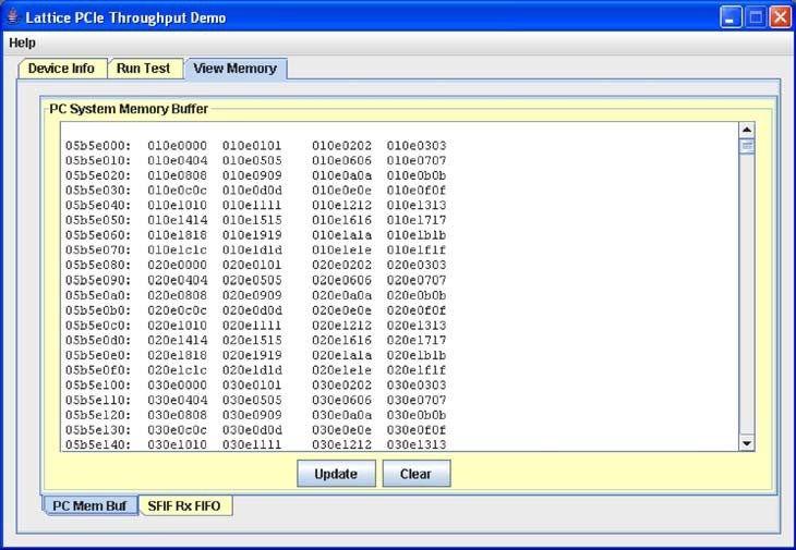
Figure 7.4. Throughput Demo View Memory Page ............................................................................................................25
Figure 8.1. DMA Demo Block Diagram................................................................................................................................28
Figure 8.2. Scatter-Gather DMA Buffer Address Mapping .................................................................................................29
Figure 8.3. ColorBars Demo Window ..................................................................................................................................30
Figure 8.4. ImageMove Demo Window ..............................................................................................................................31
Figure 8.5. ColorBars Demo Window ..................................................................................................................................32
Figure 8.6. ImageMove Program Operation Flow ..............................................................................................................33
Figure A.1. Device Manager ................................................................................................................................................35
Tables
Table 5.1. LED Order and Functionality ..............................................................................................................................10
Table 5.2. Normal x1 Link Status.........................................................................................................................................11
Table 6.1. Device Info Page Sub Tab Descriptions ..............................................................................................................14
Table 6.2. Device Info Page Sub Tab Descriptions ..............................................................................................................15
Table 6.3. Memory Page Text Box Color Codes ..................................................................................................................15
Table 6.4. Memory Page Features ......................................................................................................................................16
Table 6.5. Counter Page Features .......................................................................................................................................17
Table 6.6. Read/Write Page Features .................................................................................................................................18
Table 7.1. Device Info Page Sub Tab Descriptions ..............................................................................................................23
Table 7.2. Device Info Page Sub Tab Descriptions ..............................................................................................................24
Table 7.3. View Memory Page Sub Tab Descriptions .........................................................................................................26
Table 8.1. DMA ColorBars Demo Keyboard Commands .....................................................................................................32
Table 8.2. DMA ImageMove Demo Keyboard Commands .................................................................................................33
© 2015-2021 Lattice Semiconductor Corp. All Lattice trademarks, registered trademarks, patents, and disclaimers are as listed at www.latticesemi.com/legal.
All other brand or product names are trademarks or registered trademarks of their respective holders. The specifications and information herein are subject to change without notice.
4 FPGA-UG-02006-1.5PCI Express Demos for the ECP5 and ECP5-5G Versa Development Board
User Guide
Acronyms in This Document
A list of acronyms used in this document.
Acronym Definition
BAR Base Address Register
DMA Direct Memory Access
DPC Deferred Procedure Call
EBR Embedded Block RAM
FIFO First-In, First-Out
ICG Inter Cycle Gap
ISR Interrupt Service Routine
MRd Memory Read
MWr Memory Write
PCIe Peripheral Component Interconnect Express; PCI Express
SDRAM Synchronous Dynamic Random Access Memory
SFIF Stored FIFO InterFace
SGDMA Scatter-Gather Direct Memory Access
TLP Transaction Layer Packets
© 2015-2021 Lattice Semiconductor Corp. All Lattice trademarks, registered trademarks, patents, and disclaimers are as listed at www.latticesemi.com/legal.
All other brand or product names are trademarks or registered trademarks of their respective holders. The specifications and information herein are subject to change without notice.
FPGA-UG-02006-1.5 5PCI Express Demos for the ECP5 and ECP5-5G Versa Development Board
User Guide
1. Introduction
This guide describes how to start using the ECP5™ Versa Development Board and the ECP5-5G™ Development
Board low-cost platforms for demonstrating the PCI Express reference design and for evaluating solutions for your own
specific application. The PCI Express reference design for the ECP5 Versa Development board utilizes the Lattice
PCIE_core PCI Express Endpoint soft IP core, while the design for the ECP5-5G Versa Development board utilizes the
Lattice PCIE2_core PCI Express Endpoint soft IP core optimized for ECP5UM5G devices and 5.0 Gbps maximum transfer
rate.
Note: The PCI Express reference design for the ECP5-5G Versa Development Board does not currently support the SG-
DMA Demo.
This guide familiarizes you with the process of setting up your PCI Express development environment. This document
assumes that you do not have any associated tools installed on your system.
The demos discussed in this document include the PCI Express Basic Demo, PCI Express Throughput Demo, and PCI
Express Scatter-Gather DMA Demos (EBR).
1.1. Learning Objectives
After you complete the steps in this guide, you will be able to perform the following:
• Set up the ECP5 Versa Development Board properly and become familiar with its main features.
• Install all applicable development tools and the PCI Express demonstration applications.
• Establish communication with the ECP5 Versa Development Board through the PCI Express link.
• Run the PCI Express Basic demo that allows you to run the preset LED light sequence, interactively light LED
segments, and familiarize yourself with other features of the software.
• Run the PCI Express Throughput demo that allows you to see the performance of the Lattice PCI Express SERDES
hardware and PCI Express Endpoint IP core in terms of maximum data rates for write/read to and from your
system memory.
• Run the PCI Express Scatter-Gather DMA demos and observe how the Scatter-Gather DMA IP core, together with
the PCI Express Endpoint IP core, demonstrate data transfer between Embedded Block RAM and system memory
using the ECP5 Versa Development Board.
• Use what each demo teaches you about designing Lattice PCI Express solutions.
• Become familiar with an approach that enables you to modify and rebuild the PCI Express Basic demo for your own
purposes.
• Become familiar with the software development tools and major design flow steps employed in this kit.
• Use other existing documentation in conjunction with this guide.
This document assumes that you have already installed Lattice Diamond® design software and are familiar with basic
tasks. Otherwise, please refer to the Diamond Help system.
1.2. Related Documentation
In addition to using this guide to help you get started developing the PCI Express solution on your device, you can refer
to other associated documents that may contain more information that is beyond the scope of this guide.
The following documents can be obtained from the Lattice website:
• ECP5-5G Versa Development Board User Guide (EB103) – Describes the ECP5-5G board features, power
requirements, device programming, clock management, and board schematics in detail.
• ECP5 Versa Development Board User Guide (EB98) – Describes the ECP5 board features, power requirements,
device programming, clock management, and board schematics in detail.
• PCI Express x1/x2/x4 Endpoint IP Core User Guide (FPGA-IPUG-02009) – Describes the features that the x1, x2, and
x4 Endpoint IP Cores support and provides a functional description of the IPs, parameters, signals, port lists, timing
diagrams, memory maps, and step-by-step procedures for creating the core in Clarity Designer.
© 2015-2021 Lattice Semiconductor Corp. All Lattice trademarks, registered trademarks, patents, and disclaimers are as listed at www.latticesemi.com/legal.
All other brand or product names are trademarks or registered trademarks of their respective holders. The specifications and information herein are subject to change without notice.
6 FPGA-UG-02006-1.5PCI Express Demos for the ECP5 and ECP5-5G Versa Development Board
User Guide
• ECP5, ECP5-5G – PCI Express Demo Verilog Source Code (Basic, Throughput and Scatter-Gather DMA) User Guide
(UG106) – Provides details of the Verilog code used for each of the demos, block diagrams of the design, and
descriptions of design modules.
• ECP5 Versa Development Kit web page – Visit this web page on the Lattice web site for updates to this and other
related documents. You can download kit installation files from this page.
2. Hardware Requirements
To install the kit design and run the demo software, a single computer with a PCI Express x16, x8, x4, or x1 slot is
required. You must also have a powered USB port. All of the other hardware and drivers are included in the kit.
Note: Up to 4 GB of memory (system RAM) is supported for 64-bit systems. If you have more than 4 GB, please reduce
the memory down to 4 GB. This is due to our 32 bit drivers.
3. Software Requirements
Please be aware of the following software requirements to ensure you obtain the expected results for the procedures
described in this guide:
• The Lattice PCI Express IP demo is compatible with Microsoft Windows 7.
• The Verilog HDL demo design projects in this kit are built with Diamond version 3.5.1 or later.
• The Diamond Programmer tool is used to program the demonstration bitstreams for the ECP5. You can obtain this
software at the Diamond Programmer web page.
• To develop PCI Express designs, your computer must meet minimum system requirements as described in the
Diamond Installation Guide.
© 2015-2021 Lattice Semiconductor Corp. All Lattice trademarks, registered trademarks, patents, and disclaimers are as listed at www.latticesemi.com/legal.
All other brand or product names are trademarks or registered trademarks of their respective holders. The specifications and information herein are subject to change without notice.
FPGA-UG-02006-1.5 7PCI Express Demos for the ECP5 and ECP5-5G Versa Development Board
User Guide
4. Installing the ECP5 Versa Development Board PCI Express
Demos
To install the ECP5 Versa Development Board in Windows:
1. Go to the ECP5 Versa Development Board web page, and download the setup file: ECP5 PCI Express Demo for the
ECP5 Versa Development Kit .exe file.
2. Double-click on the DK-ECP5-PCIE[2]-setup.exe file.
3. When the Install Program as Other User dialog appears, choose to install as the current user if you have
Administrator privileges; or select another user with those privileges and click OK.
4. Click Next to start the installation. You must have administrative privileges to install the kit.
5. Click Yes to accept the license agreement.
6. Click Next to install the kit in the default C:\Lattice_DevKits location on your hard drive or install in the desired
location by using the Browse button.
7. Click Finish to complete the kit installation. Figure 4.1 shows the directory structure of the installed evaluation
board.
Default is C:\Lattice_Devkits
Kit Directory
Demo Bitstream, Drivers and Applications
Design, Bitstream, Preference, IP Files and Readme.pdf
Demo Software Source Code and Documentation
Figure 4.1. Installed ECP5 Versa Development Board Directory Structure (Windows)
Figure 4.1 shows the default installation path for Windows. Please note that whenever the kit directory or is
referred to in this document, it refers to the \DK-ECP5-PCIE-XXX\ file path, where the default
path is C:\Lattice_Devkits and XXX is the kit revision number.
© 2015-2021 Lattice Semiconductor Corp. All Lattice trademarks, registered trademarks, patents, and disclaimers are as listed at www.latticesemi.com/legal.
All other brand or product names are trademarks or registered trademarks of their respective holders. The specifications and information herein are subject to change without notice.
8 FPGA-UG-02006-1.5PCI Express Demos for the ECP5 and ECP5-5G Versa Development Board
User Guide
5. Hardware Installation
The procedures in this section provide step-by-step instructions for installing hardware and drivers to ensure proper
board and PC communication and operation.
After board setup, you can install the hardware. You must have administrative privileges on Windows to perform this
installation.
Note: Before you begin installing hardware, make sure that the demo bitstream is already loaded on the Versa Board
SPI Flash. Without the bitstream, the computer does not detect the Versa Board. See the
Running the PCI Express Basic Demo section for additional information on programming.
Caution: Lattice is not liable for any loss of data or damages that may result from the installation of the hardware and
execution of the kit demo software tools. Do not install and operate on mission-critical systems.
To install the ECP5 Versa Development Board for Windows:
1. Shut down Windows, turn off the PC and unplug the power cord.
IMPORTANT: This step is necessary because PC power supplies have voltages that are present even when the PC
power light and fan are turned off. Unplugging the PC is the safest way to ensure the board will not be hot-
swapped.
2. Locate an available PCI Express slot. The board can be installed in any slot that is larger than the finger edge in use,
x1, x4, or x16.
3. Ensure that the board is not connected to any external power supply before proceeding.
4. Using ESD precautions, install the ECP5 Versa Development Board in the PCI Express slot in the x1 position.
5. Power-on the PC and observe that it boots normally to the Windows login screen. If anything abnormal occurs,
refer to Appendix A. Troubleshooting.
6. Log in as a user with administrative privileges. During the login process Windows will detect the new hardware and
ask if you want to install it.
7. If Windows does not detect the new hardware, a restart might be necessary. Restart the computer and try again.
8. If Windows still does not detect the new hardware after a reboot, try a different PCI Express slot.
5.1. Installing Drivers
This section describes installation of the ECP5 Versa Development Board device driver software on a Windows PC. This
procedure pertains specifically to the PCI Express Basic demo application. For the PCI Express Throughput and DMA
demos, you will need to load the appropriate drivers from the respective demo folders.
Note: The Found New Hardware popup dialog in Windows appears when the PC is first booted with the board installed.
If this screen does not appear, the board was not properly detected by the PC BIOS or by Windows. Refer to Appendix A.
Troubleshooting for more information.
To install the ECP5 Versa Development Board drivers on Windows 7:
1. Go to Computer properties Device Manager. Select the PCI Express device under the Other Devices tab.
2. Right-click and choose Update Driver Software.
3. Use the Browse tab to navigate to where you have installed the demo package, locate the
Demonstration\PCIeBasic directory path on the top level of the directory, and select the Driver folder.
Note: For the PCI Express Throughput and DMA demos used in this kit, you must install the appropriate drivers
located in similar directory paths in the PCIeThruput and PCIeDMA folders, respectively.
4. Click Next. Allow the software to install by selecting Install on the pop-up window. Windows now copies the driver
files and will display a screen indicating this. Upon completion, a capital I representing initialization is displayed on
the 14-segment LED.
© 2015-2021 Lattice Semiconductor Corp. All Lattice trademarks, registered trademarks, patents, and disclaimers are as listed at www.latticesemi.com/legal.
All other brand or product names are trademarks or registered trademarks of their respective holders. The specifications and information herein are subject to change without notice.
FPGA-UG-02006-1.5 9PCI Express Demos for the ECP5 and ECP5-5G Versa Development Board
User Guide
To verify proper driver installation and device recognition on Windows:
1. Go back to Device Manager. The board (LSC_PCIexpress) should be in the list of hardware devices in your system.
2. Right-click on the Lattice evaluation board icon and select Properties to show the resources assigned to the device
and the driver information.
Memory ranges corresponding to the configured BAR registers will be assigned to the board. If this is all present, then
the demo program is able to run and access the hardware on the board.
5.2. Installing Hardware into a Different Slot
Windows identifies PCI/PCI Express hardware devices using the bus, slot, vendor ID, and device ID fields. If you install
the board into a different slot, the slot number will change. This will cause Windows to display the Found New
Hardware popup screen when the system powers up.
The full procedure described above for installing the driver is unnecessary since the driver has already been installed. If
the board is installed in a new slot, simply choose to allow Windows to search for the driver or the Install the Software
Automatically (Recommended) option and install automatically. Windows will then associate the newly created device
registry tag (bus, slot, vendor and device ID) with the lscpcie.sys driver and the demo interface will work with the board
in the new slot.
Now that your board is set up and hardware is installed on your computer, you can proceed on to the next section that
describes software installation, execution, and tasks to complete the demo.
5.3. Verifying Correct Board Operation
The section lists checks you should make to ensure proper functioning of the board. Also refer to related
documentation on this board described in ECP5 Versa Development Board User Guide (EB98) and ECP5-5G Versa
Development Board User Guide (EB103).
There are four status LED lights on the board that will go through a light sequence when the device is first powered on.
To verify the PCI Express link is functioning properly, examine these indicators at the time of powering up. The PCI
Express demonstration software used later in the kit verifies board operation. In addition, you can also check that the
status LED lights are functioning at normal conditions in the sections below.
Note: All boards leave the manufacturer fully tested. See ECP5 Versa Development Board User Guide (EB98) and ECP5-
5G Versa Development Board User Guide (EB103) for details.
5.3.1. LED Definitions
The Status LEDs on the ECP5 Versa Development Board are located vertically along the left edge, middle portion of the
board.
The LEDs are in the following order and have the following functions, as shown in the tables below.
Table 5.1. LED Order and Functionality
LED Name LED Number Color Usage
U0 D29 (x1) Red User LED. Off by default.
U1 D28(x1) Red User LED. Off by default.
U2 D27 (x1) Red User LED. Off by default.
U3 D26 (x1) Red User LED. Off by default.
DL_UP D21 (x1) Green Data Link up, ready for packets at Transaction Layer (PCI enumeration of
config registers).
L0 D22 (x1) Green L0 state active (training sequences completed; PHY Layer up and ready
for flow control).
POLL D24 (x1) Yellow Polling state inactive.
PLL D25 (x1) Yellow PLL locked to PCI Express 100 MHz clock.
© 2015-2021 Lattice Semiconductor Corp. All Lattice trademarks, registered trademarks, patents, and disclaimers are as listed at www.latticesemi.com/legal.
All other brand or product names are trademarks or registered trademarks of their respective holders. The specifications and information herein are subject to change without notice.
10 FPGA-UG-02006-1.5PCI Express Demos for the ECP5 and ECP5-5G Versa Development Board
User Guide
LED Name LED Number Color Usage
14-Segment Onboard Red 14 segment display states with letter codes as described below:
Display • I = Initialization; driver is loaded and initializes the board
• O = Open; demo program is run and driver opens access to board.
• C = Close; demo exits and driver closes access to board.
• R = Remove; driver reads that board is removed from system, as in
uninstalled device.
• E = Error; driver detects board hardware error during initialization.
14-Segment On display in Red Blinks to indicate PCI Express transaction is accessing registers or
Display Decimal lower right memory in demo IP. Indicates PCI Express bus transactions.
Point
Table 5.2. Normal x1 Link Status
PLL POLL L0 U0
Yellow Yellow Green Red
© 2015-2021 Lattice Semiconductor Corp. All Lattice trademarks, registered trademarks, patents, and disclaimers are as listed at www.latticesemi.com/legal.
All other brand or product names are trademarks or registered trademarks of their respective holders. The specifications and information herein are subject to change without notice.
FPGA-UG-02006-1.5 11PCI Express Demos for the ECP5 and ECP5-5G Versa Development Board
User Guide
6. Running the PCI Express Basic Demo
Once you have installed your ECP5 Versa Development Board in your computer and installed all necessary software,
you can run the PCI Express Basic demo which consists of hardware, IP and software. This part of the document
describes what you need to know to get started and successfully complete this demo.
6.1. Before You Begin
Before starting this demo, perform the following operations:
1. Use Diamond Programmer to download the bitstream for this demo to the board. You can find the x1 bitstream for
Diamond Programmer in the \Demonstration\PCIeBasic\Bitstreams directory path.
For general information on ECP5 programming, see ECP5 Versa Development Board User Guide (EB98) and ECP5-
5G Versa Development Board User Guide (EB103).
2. Install the board drivers for the application. You can find the driver files necessary for proper demo installation in
the \Demonstration\PCIeBasic\Driver directory path. See the procedure described in the Installing
Drivers section of this document.
6.2. Resource References
Supplementary documentation for using this demo are available.
6.2.1. Hardware Resources
The PCI Express Basic Demo x1 bitstream is built from the Diamond project located in the
Hardware\PCIe_x1\Versa_PCIeBasic\Implementation\ecp5um[5G]-45F_PCIeBasic directory. The Verilog source code
is located in the project Source\ directory.
The Verilog design architecture is explained in ECP5, ECP5-5G – PCI Express Demo Verilog Source Code (Basic,
Throughput and Scatter-Gather DMA) User Guide (FPGA-UG-02005). This document describes the purpose and
functionality of the Verilog modules used in the PCIe Demo designs.
6.2.2. Software Resources
The PCI Express Basic demo uses the lscpcie2.sys device driver. The source code for this device driver is located in
Software\lscpcie2_Win7\Driver. The architecture of the lscpcie2 device driver is explained in the lscpcie2 Driver
Reference Manual which can be accessed through the Software\PCIeDocIndex.html link.
The PCI Express Basic demo application source code is located in Software\PCIeBasic_Win2kXP\BasicGUI\DemoUI.
This directory contains the Java project source code to create the user interface. The user interface also uses the
PCIeAPI_Lib_Win2kXP API library. This code works properly for Windows 7.
The architecture of the PCIe Basic Demo application is explained in the PCIe Basic Demo Reference Manual and the
PCIe API Reference Manual which can be accessed through the Software\PCIeDocIndex.html link.
6.3. Basic Demo Operations Overview
The PCI Express Basic demo shows the capabilities of the Lattice FPGA and the PCI Express Endpoint IP core functioning
in a PCI Express slot in a Windows PC. The demo is easy to use and requires no test equipment.
This demo software allows you to access memory and registers on the board and provides real-time interaction with
the ECP5 Versa Development Board hardware to demonstrate a functional PCI Express communications path between
the application and driver software (running on the PC CPU) and the FPGA IP. Device driver and application source code
are available so you can modify and extend the behavior of the tests or use them as a starting point for new PCI Express
designs.
If you experience any problems running this demo, refer to Appendix A. Troubleshooting.
© 2015-2021 Lattice Semiconductor Corp. All Lattice trademarks, registered trademarks, patents, and disclaimers are as listed at www.latticesemi.com/legal.
All other brand or product names are trademarks or registered trademarks of their respective holders. The specifications and information herein are subject to change without notice.
12 FPGA-UG-02006-1.5PCI Express Demos for the ECP5 and ECP5-5G Versa Development Board
User Guide
6.4. Running the PCI Express Basic Demo Software
This section describes how to run the PCI Express Basic demo software after installation. You can access the PCI Express
Basic demo software by running the batch file found in the devkit installation folders.
To run the PCI Express Basic demo software by running the batch file found in the PC:
1. Browse to the Lattice_Devkits/DK-ECP5-PCIE-XXX/Demonstration/PCIeBasic directory. Run the PCIeBasic
Windows Batch File.
The graphical user interface opens the PCI Express Basic demo software with the Device Info tab activated as
shown in Figure 6.1.
Figure 6.1 provides a top-level diagram of the demo Verilog design.
Figure 6.1. PCI Express Demo Device Info Page
The Device Info page displays information about the device driver and the device’s PCI configuration registers. The data
displayed is for informational purposes only and cannot be edited. Descriptions of all of the information you can view
in this page are available in the Touring the PCI Express Basic Demo Interface section of this document.
© 2015-2021 Lattice Semiconductor Corp. All Lattice trademarks, registered trademarks, patents, and disclaimers are as listed at www.latticesemi.com/legal.
All other brand or product names are trademarks or registered trademarks of their respective holders. The specifications and information herein are subject to change without notice.
FPGA-UG-02006-1.5 13PCI Express Demos for the ECP5 and ECP5-5G Versa Development Board
User Guide
6.5. Touring the PCI Express Basic Demo Interface
This section describes the pages and features of the PCI Express Basic demo software interface.
1. In the Device Info page, click on the Device Info sub tabs and observe the structure of the information that is
displayed in each. Table 6.1 describes the information available for viewing by clicking each of the sub tabs at the
bottom of the dialog box.
Table 6.1. Device Info Page Sub Tab Descriptions
Sub Tab Page Description
Driver Info Obtained from the board PCI Config space registers by the Lattice PCI Express driver
when the demo is started. Displays Windows resources assigned to the device driver
to access the board.
Config Regs Displays the standard PCI Config type 0 registers with each field annotated.
Displaying this page causes the driver to issue PCI Config Type 0 read requests and
re-displays the register values.
Capabilities Regs Displays the PCI Express capabilities structures that are found in the register range
0x40 to 0xff. The applicable bit fields of the registers are parsed and displayed in
readable format.
Extended Regs Displays PCI Express extended configuration registers which are not used in this
demo. These are inaccessible through the PC.
2. Click on the 14 Seg tab to see the contents of the 14 Segment Control page. In this page, you will be running a
demonstration LED sequence and controlling the display on your board from this console. See Figure 6.2. The 14-
Segment Control page provides a way to interactively light segments on the display. You can preset character
sequences from this page or select single characters and run them to light the display.
The states of the LED segments are converted to a 14-bit word value (each segment is controlled by a bit) and
written to the LED control register in the GPIO portion of the IP in the FPGA. This demonstrates a memory write
across the PCI Express bus.
3. In the 14 Segment Control page, click the Run button. Notice on the board how the sequence of LED lights run in a
certain pattern on the display.
The 14-segment display has two test modes. In the first mode demonstrated here, a pre-set sequence of segments
are lit and characters are written to the display.
This LED sequence run takes approximately 30 seconds to complete. You must observe the 14-segment LEDs to see
if it is operating correctly. The correct sequence is:
a. Light all segments, one at a time, around the perimeter.
b. Light all inner segments in a clock-wise order.
c. Turn off all inner segments in reverse order.
d. Turn off all outer segments in reverse order.
e. Write the characters LATTICE* one at a time to the display.
f. The * is displayed when the test ends.
© 2015-2021 Lattice Semiconductor Corp. All Lattice trademarks, registered trademarks, patents, and disclaimers are as listed at www.latticesemi.com/legal.
All other brand or product names are trademarks or registered trademarks of their respective holders. The specifications and information herein are subject to change without notice.
14 FPGA-UG-02006-1.5PCI Express Demos for the ECP5 and ECP5-5G Versa Development Board
User Guide
Figure 6.2. PCI Express Basic Demo 14 Segment Control Page
See Table 6.2 for details about features on the 14 Segment Control page.
Table 6.2. Device Info Page Sub Tab Descriptions
Feature Description
LED Display Allows you to interactively change the LED display using mouse clicks to toggle segments on and off.
RUN Starts an LED light sequence or command operation.
SET Sets a user-defined LED light command operation based on input characters in the text box.
CLEAR Turns off all segments in the display.
4. Click on any segment in the interactive segment display in the 14 Segment Control page. Notice that any selection
will immediately cause the corresponding segment on the LED to light on your board’s LED display. Clicking on a
segment will turn it on or off (toggles). The 14-bit value written to the LED register in the FPGA is shown on the
bottom left.
5. Type any character in the text box and click the Set button. The character will be configured in the display. This
second mode of operation allows a single character to be sent to the display. Any printable ASCII character can be
displayed (lower case is displayed as upper case). You cannot write a blank character using Set.
6. Click the Clear button. This turns off all segments of the LED display. Right-clicking on the background area behind
the segments will clear the entire display.
The interactive 14 Segment Control page demonstration you just performed illustrates that a functional PCI
Express communications path exists between the application and driver software that is running on the CPU and
the FPGA IP.
7. Click on the Memory tab to open the Memory page. The Memory tab has various memory access tests that can be
run to show that the IP is accessible from host software via the PCI Express bus. See Figure 6.3. The page contains
text boxes for entering data to be sent to device registers in the FPGA design. These text boxes are color coded to
indicate the data format they accept. See Table 6.3 for details about these codes.
Table 6.3. Memory Page Text Box Color Codes
Color Code Description
Green Indicates hex value fields. Do not include any prefixes (0x) or suffixes (H). Only digits are allowable.
Yellow Indicates character string fields, e.g., ones containing file names, paths, or letter values.
Blue Indicates decimal (base 10) value fields.
The Memory Page features allow you to test the access to the 16 KB of EBR internal to the FPGA. Accesses are done on
a byte basis. All 16 KB memory locations are accessed successively, testing the PCI Express link to the memory
interface. See Table 6.4 to for a list of the actions can be performed in this page.
© 2015-2021 Lattice Semiconductor Corp. All Lattice trademarks, registered trademarks, patents, and disclaimers are as listed at www.latticesemi.com/legal.
All other brand or product names are trademarks or registered trademarks of their respective holders. The specifications and information herein are subject to change without notice.
FPGA-UG-02006-1.5 15PCI Express Demos for the ECP5 and ECP5-5G Versa Development Board
User Guide
Figure 6.3. PCI Express Basic Demo Memory Page
Table 6.4 provides descriptions of the Memory page features.
Table 6.4. Memory Page Features
Feature Description
Pattern Tests Pressing Run starts a test to check that all locations of the EBR can be read and written and that the
contents are correct. First, all 16 KB are cleared to 0 and verified. Then various patterns (AA, 55, 01, FF)
are written to all locations and verified. If everything passes, PASS is displayed. If a memory location has
an incorrect value the test aborts and displays ERRORS! The memory contents are left with an
incrementing pattern 00 01 02... that is displayed when the test successfully finishes.
READ The contents of the EBR memory are read from the value entered in the offset field. 256 bytes are read
and displayed in the list box above.
CLEAR Sets all 16 KB to 0.
FILL Writes the byte value entered in the field to all 16 KB locations.
LOAD Loads 16 KB of binary data from the file specified (or as much data as is in the file) into EBR memory,
starting at location 0. This can be used to load a known pattern into the EBR memory by using a file
created by another tool.
SAVE Writes all 16 KB of EBR memory to the file specified. This can be used to save the contents of EBR
memory for off-line processing (that is, to verify that the pattern loaded in with LOAD is correctly saved
in the EBR).
8. Click on the Counter tab to open the Counter page. The Counter page allows you to control a 32-bit down counter
in the FPGA hardware. The page is illustrated in Figure 6.4. Table 6.5 provides descriptions of the page’s features.
The counter is driven by the 125 MHz clock that feeds the IP. The counter is started by selecting the Start radio
button. Counting begins from the value entered into the Reload Value field. The current count value is displayed in
the Current Count field.
© 2015-2021 Lattice Semiconductor Corp. All Lattice trademarks, registered trademarks, patents, and disclaimers are as listed at www.latticesemi.com/legal.
All other brand or product names are trademarks or registered trademarks of their respective holders. The specifications and information herein are subject to change without notice.
16 FPGA-UG-02006-1.5PCI Express Demos for the ECP5 and ECP5-5G Versa Development Board
User Guide
Figure 6.4. PCI Express Basic Demo Counter Page
Table 6.5 provides descriptions of all of the Counter page features.
Table 6.5. Counter Page Features
Feature Description
START/STOP Starts and stops the 32-bit down counter in the FPGA hardware.
Current Count Displays the current count value.
Reload Value Sets the number from which countdown begins.
DIP Switch The DIP switch section shows that user changes to the switches on the board are seen by the
application software on the PC. The GUI polls the DIP switch register 10 times per second and displays
the value read from the 8-bit DIP switch register.
Get button Used to immediately update the value. This is active if No Polling was selected from the Settings drop-
down menu.
9. Finally, click on the Rd/Wr tab to open the Read/Write page. The Read/Write page is used for looking at and
poking at registers and EBR memory values in the application IP. Refer to Figure 6.5.
© 2015-2021 Lattice Semiconductor Corp. All Lattice trademarks, registered trademarks, patents, and disclaimers are as listed at www.latticesemi.com/legal.
All other brand or product names are trademarks or registered trademarks of their respective holders. The specifications and information herein are subject to change without notice.
FPGA-UG-02006-1.5 17PCI Express Demos for the ECP5 and ECP5-5G Versa Development Board
User Guide
Figure 6.5. PCI Express Basic Demo Read/Write Page
The Read/Write page is primarily used for debugging and diagnosing the application IP registers. Table 6.6 provides
descriptions of all of the Read/Write page features.
Table 6.6. Read/Write Page Features
Feature Description
Memory Space Indicates the Base Address Register (BAR) memory space to access.
Data Size Indicates bit size. Options are 8-bit, 16-bit, and 32-bit.
Memory Contents Displays memory contents.
READ Starts a read data access based on offset and length settings.
WRITE Starts a write data access based on offset and data settings.
Data accesses can be specified as byte, short or word operations by selecting Data Size. Access is done to the selected
BAR. The memory contents are displayed in the window. In the address, the upper nibble (31:28) specifies the BAR
being accessed. The following example shows reading the EBR memory (BAR 1, starting at offset 0x1000) in the
application IP and displaying them in word format.
Data can be written to registers using the WRITE button. Specify the BAR Offset to start writing at and the hex data in
the Data field. Separate each value with a space. Data size should match the Data Size selected at the top of the page in
Memory Settings.
6.6. Rebuilding the PCI Express Basic Demo Design
You can rebuild the PCI Express Basic demo IP reference design by running the source HDL design files through a design
flow in the Diamond software. All source HDL files and necessary project files are included in the kit installation. This
document assumes that you have already installed Diamond and are familiar with basics tasks. Refer to Figure 4.1 to
understand where various files referenced in this section are located.
We recommend that you copy the files from the installation location to a new working location. This allows you to
quickly move back to the original configuration without re-installing this kit.
© 2015-2021 Lattice Semiconductor Corp. All Lattice trademarks, registered trademarks, patents, and disclaimers are as listed at www.latticesemi.com/legal.
All other brand or product names are trademarks or registered trademarks of their respective holders. The specifications and information herein are subject to change without notice.
18 FPGA-UG-02006-1.5PCI Express Demos for the ECP5 and ECP5-5G Versa Development Board
User Guide
6.6.1. Implementing the PCI Express Basic Demo Design
The top.ldf Diamond project file is included in this kit. This file contains information regarding options to use when
implementing the demo design. The top.lpf logical preference file specifies timing constraints and ECP5 I/O pin
assignments with respect to the ECP5 Versa Development Board. The working directory is the implementation
directory.
To implement the demo design using the HDL source flow:
1. Open Diamond.
2. Click File > Open Project.
3. In the Open Project dialog box, navigate to and select the top.ldf file in the
\Hardware\PCIe_x1\Versa_PCIeBasic\Implementation\ecp5um-45f_PCIeBasic directory path.
4. Click Open. All of the Verilog HDL files are imported into the project.
5. Choose Project > Active Strategy > Translate Design Settings. Verify that Macro Search Path is set to the directory
path .../Clarity/ecp5/pcie_core/pcie_x1 for Windows. Click OK.
6. In the File List pane of Diamond, right-click the device name at the top of the list, and chose Properties from the
drop-down menu.
7. In the Project Properties dialog box, make sure that the following properties are selected: ECP5 family, LFE5UM-
45F device, -7 speed grade, and a CABGA381 package. Click OK.
8. In the Process pane of Diamond double-click on the Bitstream file.
6.7. Modifying the PCI Express Basic Demo Design
This section provides a simple alteration to the HDL to demonstrate a change in the behavior of the function of the LED
light in the demo display. It will involve a small change in the HDL code in the source file.
Note: Since the source is being changed, the resulting netlist may be different and the provided start point for Place &
Route may no longer produce a design that meets timing. Running more iterations to achieve timing may be required.
See the Place & Route Properties.
To modify the PCI Express Basic demo design:
1. Open the top_basic.v file with an ASCII editing tool or the internal ASCII editing tool in Diamond. This file is located
in the Save and close the editor.
This modification to the code causes the 14-segment LED to operate in reverse, that is, when the demo starts, all
the lights will be on instead of off.
4. Open the top.ldf project file in Diamond. This file is located in the folder below:
Hardware\PCIe x1\Versa_PCIeBasic\Implementation\ecp5um-45F_PCIeBasic .
5. Double click the Bitstream File process in the Processes window to generate a top.bit file in the directory
\Hardware\Implementation.
6. Start Diamond Programmer and perform the steps described in the Reprogramming the ECP5 Versa Development
Board to download the new bitstream to the board’s SPI flash memory.
7. Push the PROGRAM button on the board to program your device from SPI Flash memory.
8. Reboot the PC so that the BIOS recognizes the new PCI Express endpoint device configuration.
9. Verify that the status LEDs are correct and note that all the LED segments are now on.
© 2015-2021 Lattice Semiconductor Corp. All Lattice trademarks, registered trademarks, patents, and disclaimers are as listed at www.latticesemi.com/legal.
All other brand or product names are trademarks or registered trademarks of their respective holders. The specifications and information herein are subject to change without notice.
FPGA-UG-02006-1.5 19PCI Express Demos for the ECP5 and ECP5-5G Versa Development Board
User Guide
10. Rerun the LED test described in the Touring the PCI Express Basic Demo Interface section of this document.
Notice that the state of the 14-segment LED on the board is the inverse of what is displayed in the user interface.
You have now completed the Lattice PCI Express Basic demo and have successfully completed all of the learning
objectives of this kit.
© 2015-2021 Lattice Semiconductor Corp. All Lattice trademarks, registered trademarks, patents, and disclaimers are as listed at www.latticesemi.com/legal.
All other brand or product names are trademarks or registered trademarks of their respective holders. The specifications and information herein are subject to change without notice.
20 FPGA-UG-02006-1.5PCI Express Demos for the ECP5 and ECP5-5G Versa Development Board
User Guide
7. Running the PCI Express Throughput Demo
This chapter describes the Lattice PCI Express Throughput demo that you can run within this kit on a Windows 7
system.
7.1. Before You Begin
Before starting this demo, perform the following operations:
1. Use Diamond Programmer to download the bitstream for this demo to the board. You can find the x1 bitstream
necessary for Diamond Programmer in the \Demonstration\PCIeThruput\Bitstreams directory path.
For general information on ECP5 programming, see ECP5 Versa Development Board User Guide (EB98) and ECP5-
5G Versa Development Board User Guide (EB103).
2. Install the board drivers for the application. You can find the driver files necessary for proper demo installation in
the \Demonstration\PCIeThruput\Driver directory path. See the procedure described in the Installing
Drivers section of this document.
7.2. Resource References
Supplementary documentation for using this demo are available.
7.2.1. Hardware Resources
The PCI Express Throughput Demo x1 bitstream is built from the Diamond project located in the
Hardware\PCIe_x1\Versa_PCIeThruput\Implementation\ecp5um[5G]-45F_PCIeThruput directory. The Verilog source
code is located in the project Source\ directory.
The Verilog design architecture is explained in ECP5, ECP5-5G – PCI Express Demo Verilog Source Code (Basic,
Throughput and Scatter-Gather DMA) User Guide (FPGA-UG-02005). This document describes the purpose and
functionality of the Verilog modules used in the PCIe Demo designs.
7.2.2. Software Resources
The PCI Express Throughput demo uses the lscpcie2.sys device driver. The source code for this device driver is located
in Software\lscpcie2_Win7\Driver. The architecture of the lscpcie2 device driver is explained in the lscpcie2 Driver
Reference Manual which can be accessed through the Software\PCIeDocIndex.html link.
The PCI Express Throughput demo application source code is located in
Software\PCIeSFIF_Win2kXP\SFIF_GUI\SFIF_UI. This directory contains the Java project source code to create the user
interface. The user interface also uses the PCIeAPI_Lib_Win2kXP API library. This code works properly for Windows 7.
7.3. Throughput Demo Operations Overview
The purpose of this demo is to show the performance of the Lattice PCI Express SERDES hardware and PCI Express
Endpoint IP core when operating in a PC PCI Express expansion slot. The data rates for writes to the PC system memory
and reads from the PC system memory are measured and displayed in a graphical user interface.
The demo performs Direct Memory Access (DMA) operations by transferring data directly to and from the PC memory.
The demo uses an IP block named the SFIF (Stored FIFO InterFace) to generate read and write Transaction Layer
Packets (TLPs) that will access the PC system memory. The SFIF exercises the PCI Express Endpoint IP core and link with
low overhead so the true performance of the PCI Express core and link can be measured.
The PCI Express interface is used for both control plane and data plane traffic. The control plane loads the SFIF memory
and sets up the transfer. The data plane transfers the data from the SFIF to the PC memory. Figure 7.1 shows the
relationship of the hardware and software components of the demo. For more details on SFIF IP, register mapping and
related topics, see PCI Express x1/x2/x4 Endpoint IP Core User Guide (IPUG112) and ECP5, ECP5-5G – PCI Express Demo
Verilog Source Code (Basic, Throughput and Scatter-Gather DMA) User Guide (FPGA-UG-02005).
© 2015-2021 Lattice Semiconductor Corp. All Lattice trademarks, registered trademarks, patents, and disclaimers are as listed at www.latticesemi.com/legal.
All other brand or product names are trademarks or registered trademarks of their respective holders. The specifications and information herein are subject to change without notice.
FPGA-UG-02006-1.5 21You can also read