Nanowires for 2D material-based photonic and optoelectronic devices
←
→
Page content transcription
If your browser does not render page correctly, please read the page content below
Nanophotonics 2022; 11(11): 2571–2582

Review

Ha Young Lee and Sejeong Kim*

Nanowires for 2D material-based photonic and
optoelectronic devices
https://doi.org/10.1515/nanoph-2021-0800                                       focused on improving the strength of light–matter inter-
Received December 20, 2021; accepted January 26, 2022;                         action in order to realise compact integrated photonic
published online February 8, 2022                                              circuits [1–3], efficient photonic devices [4, 5], and multi-
                                                                               functioning optoelectronic systems [6, 7]. 2D materials are
Abstract: Nanowires have garnered considerable atten-
                                                                               one of the most vigorously investigated materials in mod-
tion in photonics and optoelectronics due to their unique
                                                                               ern science. There are various advantages of using 2D
features. Owing to the large surface area and significant
                                                                               materials for research. For example, 2D materials provide
potential of usage as a resonator and waveguide in pho-
                                                                               favorable mechanical properties such as being highly
tonic integrated circuits (PICs), nanowires have been
                                                                               bendable and stretchable without causing damage [8].
applied in many research areas in nanophotonics. To
                                                                               Additionally, one can easily create atomically smooth,
enhance the properties of light emitting materials, the
                                                                               mono- or few layered samples by simply exfoliating 2D
hybrid of nanowires and 2D materials has been deployed in
                                                                               materials from the bulk crystal using a sticky tape, which
many papers. This paper summarises recent studies on the
                                                                               has increased the use of 2D materials for laboratory study.
application of various types of nanowires in photonics and
                                                                               Through the exfoliation method, 2D materials can be
optoelectronics, as well as the combination of nanowires
                                                                               transferred or stacked onto any materials without regard
and 2D materials. This review article introduces nanowires
                                                                               for lattice-mismatch concern. So far, researchers have
that act as resonators or/and waveguides to increase
                                                                               identified a library of 2D materials with characteristics
the performance of 2D materials used in PICs for light
                                                                               ranging from metals to insulators, and these materials
enhancement and guiding. Moreover, the review lays out
                                                                               sometimes exhibit unique properties such as high elec-
the hybrid of nanowires and 2D materials that have been
                                                                               trical conductivity [9], high nonlinearity [10, 11] or valley-
studied in the field of optoelectronics. The hybridization of
                                                                               dependent electrical/optical response [12].
nanowires and 2D materials for photonics and optoelec-
                                                                                    The hybridization of nanowires with 2D materials
tronics is discussed in this review for the outlook of future
                                                                               enables 2D materials to function better as a photonic and
studies.
                                                                               electrical device. Nanowires can be made of metals, semi-
Keywords: 2D materials; integrated photonic circuits;                          conductors or insulators. Metal nanowires are versatile since
nanophotonics; nanowires; optoelectronics.                                     they can be used as both electrodes and photonic compo-
                                                                               nents. Silver is frequently adopted as an electrode material
                                                                               due to its high transmittance, low sheet resistance and high
                                                                               flexibility. By incorporating 2D materials such as MXene,
1 Introduction                                                                 graphene, or graphene oxide [13], one can address some of
                                                                               the bottlenecks that impeding their practical usage. For
The study of the interaction of light and matter has gained
                                                                               example, 2D conducting layers connects nanowires and
popularity for several decades. Recent emphasis has been
                                                                               smooth out the surface, resulting in reduced resistance. In
                                                                               addition, 2D insulating materials protect metal nanowires
*Corresponding author: Sejeong Kim, Department of Electrical and               from oxidation. These heterostructures can be in various
Electronic Engineering, Faculty of Engineering and Information                 configurations as described in Figure 1. Besides electrodes,
Technology, University of Melbourne, Victoria 3010, Australia,                 metal nanowires act as waveguides [14], open nanocavities
E-mail: sejeong.kim@unimelb.edu.au. https://orcid.org/0000-0001-               [15], and control light emission properties [16]. As semi-
9836-3608
                                                                               conductor manufacturing technology progresses [17], semi-
Ha Young Lee, Department of Electrical and Electronic Engineering,
Faculty of Engineering and Information Technology, University of
                                                                               conductor nanowires are widespread and play an important
Melbourne, Victoria 3010, Australia. https://orcid.org/0000-0002-              role as a platform for integrated photonic circuits [18]. One
3528-183X                                                                      significant advantage of semiconductor nanowires is their
  Open Access. © 2022 Ha Young Lee and Sejeong Kim, published by De Gruyter.           This work is licensed under the Creative Commons Attribution 4.0
International License.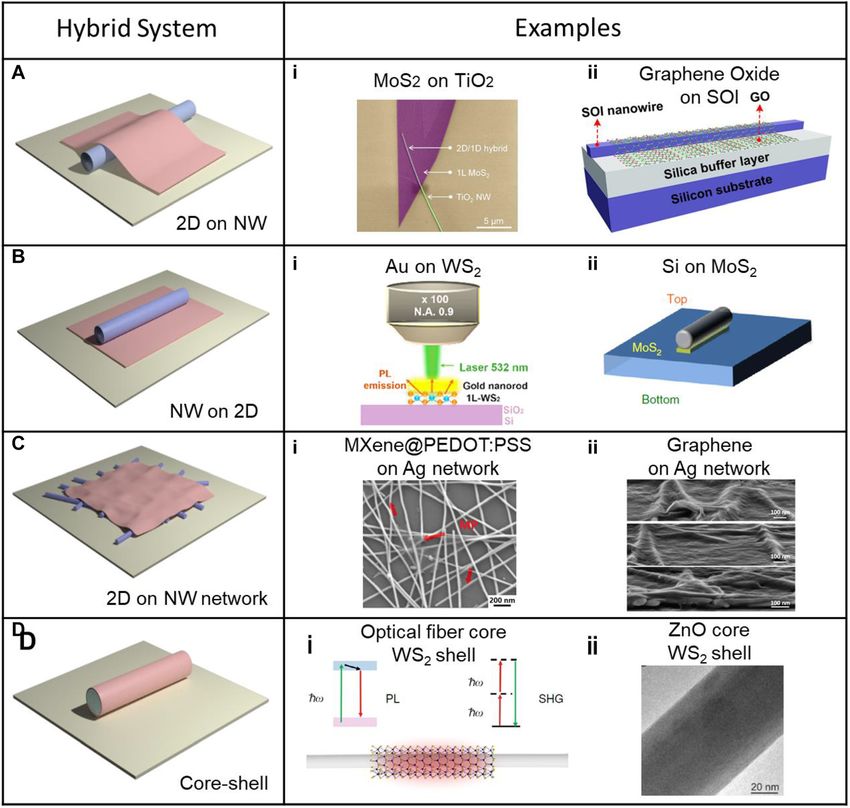
2572          H.Y. Lee and S. Kim: NWs for 2D devices

compatibility with complementary metal–oxide–semi-                      core–shell or nanowire-on-monolayer structures, a syner-
conductor (CMOS) technology while yet providing advanced                getic effect is anticipated.
electrical and optical functionality [19, 20]. When these                    2D materials are also being investigated in quantum
nanowires are combined with 2D materials in the form of                 photonics as a promising quantum light source. For

Figure 1: Schematic of the hybridization of nanowires and 2D materials.
(A) 3D structure diagram of a 2D on a nanowire. (A-i) False-color SEM image of a monolayer MoS2/NW hybrid structure. Reproduced/adapted
with permission from Li et al. [21]. Copyright 2019 American Chemical Society. (A-ii) Schematic of a GO-coated on an SOI nanowire waveguide.
Reproduced/adapted with permission from Zhang et al. [22]. Copyright 2020 American Chemical Society. (B) 3D structure diagram of a
nanowire on a 2D material. (B-i) Schematic showing photoluminescence measurement of a gold nanorod on a monolayer WS2 heterostructure.
Reproduced/adapted with permission from Jiang et al. [23]. Copyright 2020 American Chemical Society. (B-ii) Schematic of a silicon nanowire
on a MoS2 layer. Reproduced/adapted with permission from Cihan et al. [19]. Copyright 2018 Macmillan Publishers Limited, part of Springer
Nature. (C) 3D structure diagram of a 2D material covering a nanowire network. (C-i) SEM image of AgNW-MXene@PEDOT:PSS hybrid.
Reproduced/adapted with permission from Bai et al. [24]. Copyright 2020 Elsevier Ltd. (C-ii) SEM images of EG thin layer on AgNWs network.
Reproduced/adapted with permission from Ricciardulli et al. [25]. Copyright 2018 Wiley-VCH Verlag GmbH & Co. KGaA, Weinheim. (D) 3D
structure diagram of a nanowire-core/2D material-shell. (D-i) Schematic of a hybrid WS2-optical-fiber-nanowire. Reproduced/adapted with
permission from Chen et al. [26]. Copyright 2019 by the original authors (CCBY). (D-ii) TEM image of ZnO/WS2 nanowire annealed in sulfur
atmosphere and additionally annealed in an inert atmosphere. Reproduced/adapted with permission from Butanovs et al. [27]. Copyright
2018 American Chemical Society.
H.Y. Lee and S. Kim: NWs for 2D devices 2573
example, 2D semiconducting material such as WS2 and results in increased resistance due to cracks when bending
MoS2 monolayers and 2D insulating material such as hex- the substrate [41]. Additionally, indium is a scarce raw
agonal boron nitride (hBN) have single photon emitters. By material in the Earth’s crust, necessitating the use of sub-
incorporating nanowires, one can control the single stitute materials. Metal nanowires are promising candi-
photon emission and route it through the nanowires. 2D dates due to their exceptional optical and electrical
materials are also used to study second-harmonic genera- properties [42, 43]. They demonstrated attractive features
tion (SHG) [21], and reduction of undesired emission is and are expected to replace ITO in commercial applications
reported [19] by implementing semiconductor nanowires. [44, 45]. This is because they are resilient to bending and
Additionally, WS2 monolayers are widely used on photo- folding cracks due to the increased elasticity provided by
detectors. The hybrid of the WS2 layer with ZnO [27] or CdS nanostructures while maintaining good electrical con-
[28] nanowire was proven to have higher responsivity, ductivity and optical transparency [46, 47].
faster operation, and higher absorption of light through However, metal nanowires retain certain inherent
band alignment induced charge carrier transfer. Also, weaknesses, including high degree of surface roughness
perovskite nanowires including CsPbBr3 have high [48], low adhesion to the substrate, discontinuous struc-
potentials for application in piezotronic [29] and piezo- ture between interface of nanowires [24] and fast degra-
phototronic devices [30, 31]. Moreover, their optical dation. These issues can be overcome by adding additional
properties could be enhanced when incorporated with materials, i.e., creating a hybrid system. These hybrid
transition metal dichalcogenides (TMDs) materials. This is systems consist of 2D materials with properties that are
by enabling effective charge carrier transfer through the applicable in overcoming the problems. For example,
WS2 conducting channel while also suppressing dark cur- MXene, a 2D material that consists of transition metal
rent. WS2 monolayer is also integrated with optical fiber for carbide, nitride, and carbonitride [49, 50], is frequently
enhancement of SHG by evanescent field coupling [26]. used to mitigate the problems. MXene is widely explored
This article summarises the role of micro/nanowires in 2D material in the fields of sensors [51] and transparent
photonics and electronics. This article first discusses the electrodes [52] due to its features such as high electrical
use of nanowires as electrodes. Nanowires are advanta- conductivity and large surface area. Graphene is also one
geous as electrodes due to their high conductivity and of the promising 2D materials in this regard due to its
flexibility. Then we expand the discussion to include their unique electrical and optical properties [53].
applications in photonics and electronics. Nanowires can Bai et al. [24] addressed issues relating to nanowire
operate as a photonic resonator and a waveguide, which FTE by covering them with MXene, which effectively re-
aid in understanding how nanowires can enhance the duces the surface roughness of the nanowires. Using this
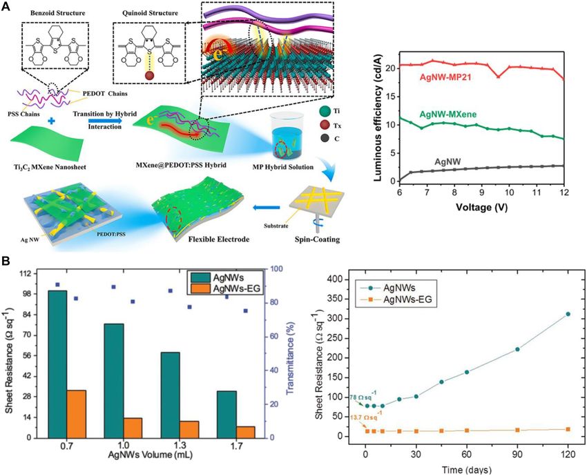
functionality of photonics and electronics devices. approach, they achieved a low sheet resistance of 17 Ω/sq
and high transmittance of 97.6% at λ = 550 nm. In detail, 2:1
mass ratio of Ti3C2Tx MXene and PEDOT:PSS hybrid solu-
tion (denoted as MP21) were diluted with DI water and
2 Conventional applications: stirred at room temperature for 2 h and it was spin-coated
nanowires as electrodes onto Ag nanowire FTE as shown in Figure 2A. As a result,
MXene nanosheets covering Ag nanowire networks
Flexible and transparent electrodes are desirable for a reduced surface roughness of Ag NW, and PEDOT:PSS
variety of applications and are expected to find a wide polymer filling the hollow regions of Ag NW acted as a
range of usage in optoelectronics [32, 33]. Such electrodes nanowelding process, reducing junction resistance. To
have been used in flexible organic light-emitting diode investigate the light emitting performance and current ef-
(FOLEDs) [34, 35], solar cells [36], and many other opto- ficiency of the sample, red FOLEDs were fabricated using
electronic applications [37, 38]. Metal nanowires are the synthesized material. Compared to bare NW and
particularly attractive for the development of flexible NW-MXene, the Ag nanowire with MXene and PEDOT:PSS
transparent electrodes (FTE) due to their high trans- hybrid has improved on the aspect of luminance and cur-
mittance and low sheet resistance [39, 40]. Traditionally, rent efficiency. The luminescence efficiency-voltage char-
indium tin oxide (ITO) has been a widely adopted material acteristics of Ag NW, Ag NW-MXene, and Ag NW-MP21 FTE
for flexible and transparent electrodes. ITO has a high based red FOLED were tested (Figure 2A). AgNW-MP21
conductivity while being transparent at visible wave- based FOLEDs achieved the highest luminance efficiency
lengths. However, there are several drawbacks to of over 21 cd/A and a maximum external quantum effi-
employing ITO, including poor mechanical stability, which ciency (EQE) of 25.9%.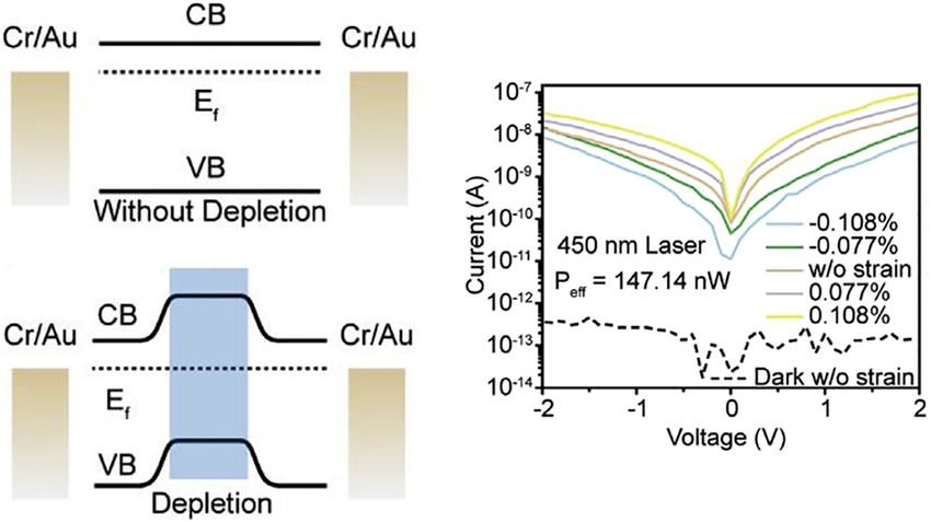
2574          H.Y. Lee and S. Kim: NWs for 2D devices

Figure 2: Integration of metallic NW and 2D materials for the flexible transparent electrodes.
(A) Left, schematic illustration of the fabrication process of AgNW-MXene@PEDOT:PSS hybrid FTEs. Right, luminous efficiency of AgNW,
AgNW-MXene hybrid, and AgNW-MP21 hybrid FTEs on silicon. Reproduced/adapted with permission from Bai et al. [24]. Copyright 2020
Elsevier Ltd. (B) Left, sheet resistance and transmittance of AgNWs and AgNWs-EG films at different AgNWs volumes. Right, long term sheet
resistance of AgNWs and AgNWs-EG with air exposure. Reproduced/adapted with permission from Ricciardulli et al. [25]. Copyright 2018
Wiley-VCH Verlag GmbH & Co. KGaA, Weinheim.

     Similarly, graphene has been adopted to improve the              lower the sheet resistance (Rs) without noticeable decrease
conductivity of electrodes in hybrid systems. Ricciardulli            of transmittance and simultaneously decreased the
et al. [25] demonstrated transparent electrodes composed              roughness from 78 Ω/sq to 13.7 Ω/sq and from 16.4 to
of silver nanowires and electrochemically exfoliated gra-             4.6 nm, respectively. Lowered sheet resistance and
phene (EG). In detail, the solution containing silver nano-           roughness was due to the EG coating as the dispersed layer
wires is first sprayed onto flexible substrate, polyethylene            flattened the surface of the Ag NW junctions and holes. This
naphthalate (PEN), followed by EG dispersion. In                      paper further demonstrated the implementation of the
Figure 2B, sheet resistance and transmittance of various              electrode as an anode in an organic solar cells (OSC) and
volume of silver nanowires with the EG layer are compared             polymer LEDs (PLEDs).
with the pristine Ag nanowires. Moreover, the samples                     2D materials not only decrease the surface roughness,
were exposed in the air for 120 days for long-term stability          but also play an important role as a protective layer that
(Figure 2B). During those times, the sheet resistance of the          prevents metal nanowires from oxidization. Silver nano-
hybrid material remained constant while that of the                   wire, which is one of the most frequently used metal wires
pristine sample increased after 10 days of exposure. They             as a bottom electrode of perovskite solar cells (PVSC) has
reported that by deploying the EG layer, they were able to            corrosion issues caused by the release of halide species
H.Y. Lee and S. Kim: NWs for 2D devices 2575
from the perovskite layer [54]. Chen et al. [13] proposed the includes lasing in cesium lead halide perovskite nanowires
implementation of large-size graphene oxide (LGO) sheets [56] and single mode lasing from CdS nanowires [57]. Apart
as a protective layer for silver nanowire-based transparent from FP mode, microwires with a diameter in the micro-
electrodes. LGO sheets acting as protective layers are meter range can allow whispering gallery mode (WGM)
crucial to reduce the overall boundary area, as boundaries [58]. Therefore, an appropriate radius should be selected
between the sheets lets in halide species. In this work, GO based on the optical modes to be used.
sheets with different sizes are separated by centrifugal Another frequently adopted geometry for nanowire
method. The reduced LGO dispersion was dropped on the devices are nanowire-gap-substrate structure, which is
Ag NW electrode and dried using steady hot air flow. The used to facilitate gap mode. To achieve a gap mode, the gap
electrode maintained its initial resistance for more than layer is made of a thin dielectric material while nanowire or
45 h while the pristine sample exhibited exponential in- substrate, or both, are made of metal. This gap mode
crease of resistance after 10 h at 0.8 V bias. This study enables tight light focusing, which increases the Purcell
demonstrates the possibility of constructing PVSC with factor, which is defined as the Q-factor divided by the mode
high stability. volume. Therefore, nanowire-gap-substrate geometry is
often used for nanowire lasing experiments. As an
example, Xiang Zhang’s group [59] experimentally
3 Nanowire as a versatile platform demonstrated a nanoscale plasmonic laser with optical
mode smaller than the diffraction limit using CdS semi-
for nanophotonics conductor nanowire, separated from a silver surface by an
insulating gap.
Nanowires offer a wide range of applications in photonics Apart from the cavity effect, both dielectric and
and electronics as they operate as a resonator and a metallic nanowires have the potential to act as wave-
waveguide. Mechanisms for nanowire working as a cavity guides. Dielectric waveguides have a lower loss than
and a waveguide are summarized in recent review paper by metallic waveguides. Meanwhile, metallic nanowires on
Z. Gu et al. [55]. Nanowires are Fabry–Perot (FP) type res- dielectric material or dielectric nanowire on metal sub-
onators that are composed of two mirrors that confine strate can be relatively lossy because they convey the light
standing waves. In bulk optics, optical resonators are signal using surface plasmon polariton. The following
typically constructed using two mirrors with near-unity section will cover nanowires for 2D materials. Nanowires
reflectivity (R); however, nanowires built of semiconductors can be used to increase the PL intensity of 2D TMDs via the
or dielectric materials take use of the reflection induced by cavity effect and to guide the emission from 2D materials
a change in the refractive index (n). The reflectivity at via the waveguide effect. Additionally, the paper will
the interface of two materials having refractive index of n1 outline a hybrid system composed of nanowires and two-
and n2 is determined by the Fresnel’s equation: dimensional materials for use as a quantum light source
2 and photon detector.
n2 − n1
R=( )
n2 + n1
The Q-factor (Q) of the FP type cavity is as follows: 4 Nanowires for 2D materials
2πnL
Q= 4.1 Light enhancement
λ(1 − R)
Therefore, it is preferable to have a longer wire length By increasing the spontaneous emission (SE) rate of radi-
(L) and a high refractive index at the incident wavelength ative emission of light emitting 2D materials, a brighter
(λ) to maximize light confinement. Numerous studies have light source can be created. The ratio of SE rate with and
been published in which nanowires have been used as the without a cavity is called Purcell factor, and it is propor-
FP cavity. What’s noteworthy is that semiconductor tional to Q-factor and inversely proportional to the optical
nanowires are a complete nanolasers consisting of an mode volume. Many approaches have been made to ach-
optical resonator and a gain medium. Due to the ease of ieve high PL intensity and this can be realized by using
fabrication complexity in comparison to other type of hybridization of nanowires with TMDs. Utilizing nanowires
nanolasers that requires photo or electron-beam lithog- is also a popular approach for optical anisotropy [60, 61].
raphy, semiconductor nanowires have been attracting By tuning the morphology of the nanostructure, resonance
considerable attention. Some of the recent lasing work frequency and quality factors could be controlled. With the2576 H.Y. Lee and S. Kim: NWs for 2D devices
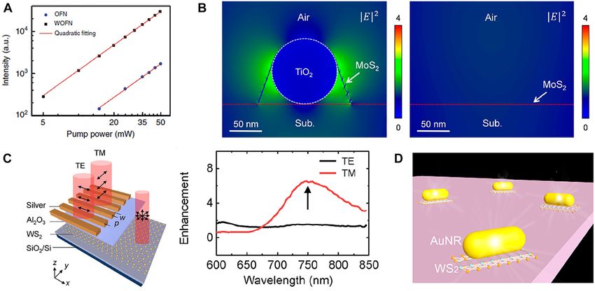
incorporation of 2D TMDs with plasmonic or optical field of MoS2. The lattice deformation of the MoS2 layer
nanowires, effective control and enhancement of light induced by the nanowire broke the 3-fold crystal symmetry
could be made into practical use. of MoS2 and this deformation led to the anisotropic SHG
The hybrids of nanowires and 2D TMDs are applied in enhancement. This study illustrates the possibility of tun-
various applications for the enhancement of light–matter ing SHG intensity and polarization by introducing and
interactions. Chen et al. [26] used a hybrid of optical adjusting nanowires to the TMDs layer.
fiber nanowire and WS2 for efficient second harmonic Furthermore, Han et al. [62] demonstrated anisotropic
generation (SHG). Instead of the free-space coupling enhancement of PL by employing a hybrid system of
technique for SHG, the study employed an optical wave- plasmonic nanowire arrays and WS2. WS2 flakes were
guide technique to enhance the conversion efficiency. The grown through chemical vapor deposition (CVD) and
WS2-optical-fiber-nanowire (WOFN) was fabricated by nanowire arrays were fabricated on top using electron-
laminating a WS2 monolayer on an OFN using a modified beam lithography and silver metallization. The device was
microtransfer technique. On Figure 3A, the SHG intensity characterized through polarization-resolved PL imaging.
as a function of pump power was measured. The WOFN The PL images of the TE and TM polarized light showed that
showed a 20 times higher amount of the SHG intensity the hybrid area of nanowire arrays and bilayer WS2 had
compared to that of the OFN. By the evanescent field significant enhancement for both modes at indirect
coupling effect in the OFN, the enhancement of light–matter bandgap transition region, when compared to the pristine
interaction can be expected. WS2 (Figure 3C).
Moreover, Li et al. [21] showed anisotropic enhance- In addition, Jiang et al. [23] integrated monolayer of
ment of SHG by integrating a MoS2 layer with TiO2 nano- WS2 flake with plasmonic Au nanorod for PL enhancement.
wires. The SHG emission from the hybrid material The study designed a heterostructure of a gold nanorod on
displayed an enhanced signal of more than two orders of top of a WS2 monolayer. The monolayer was fabricated
magnitude due to the intensified local electric field as same as the size of the projected area of the nanorod as can
shown on Figure 3B. The pattern of SHG varied by the strain be seen on Figure 3D. The design was to suppress the
Figure 3: Hybrids of NW and 2D TMDs for the enhancement of light–matter interactions.
(A) Second harmonic generation intensity as a function of the pump power for the OFN and WOFN. Reproduced/adapted with permission from
Chen et al. [26]. Copyright 2019 by the original authors (CC BY). (B) Calculated electric field distribution (|E|2) excited by the fundamental wave
(λ = 800 nm) in: MoS2/NW hybrid (left) and pristine MoS2 film (right). Reproduced/adapted with permission from Li et al. [21]. Copyright 2019
American Chemical Society. (C) Left, schematic of the hybrid device. Right, PL enhancements of the hybrid material relative to the pristine WS2
for TE and TM polarizations. Reproduced/adapted with permission from Han et al. [62]. Copyright 2021 by the original authors (CC BY). (D)
Schematic of the heterostructure composed of a gold nanorod integrated on top of a WS2 monolayer. Reproduced/adapted with permission
from Jiang et al. [23]. Copyright 2020 American Chemical Society.H.Y. Lee and S. Kim: NWs for 2D devices 2577
background PL and to solely monitor the PL of the heter- 5 Optoelectronics
ostructure. The study showed PL enhancement compared
to that of the pristine monolayer WS2. These studies Many applications of 1D/2D hybrid materials have been
show promising applications on tunable ultrathin pho- carried out in the field of optoelectronics such as photo-
tonic devices. detectors, light emitting diodes (LEDs) and photo-
transistors. Utilization of 1D/2D hybrid materials are one of
the attractive viewpoints on these applications. Among
4.2 Light guiding these applications, photodetectors have gained a lot of
attention in the last few years due to their appealing
Effective control of radiation properties of light emitters is application in various fields [67–69]. One of the popular
crucial in developing integrated photonic circuits. Various strategies is to implement materials that are functionalized
approaches have been made to make use of these charac- by nanomaterials [70–72], or to modify their chemical or
teristics [63, 64]. For instance, Lin et al. [65] introduced morphological properties to enhance the output of their
coupled plasmonic waveguide with improved efficiencies applications [73, 74]. Also, using heterojunction of a bulk
that can lighten the trade-off such as confinement loss. or nanomaterials is a popular method developed for high-
Nanowires with 2D materials are also widely used in the performance photodetectors [75–79]. These hybrid mate-
field of light guiding. rials showed noticeable improvement on their responsivity
Zhang et al. [20] theoretically studied and optimized compared to their counterparts. The comparison can be
the Kerr nonlinear optical performance of silicon-on- seen on Table 1 [27, 28, 30, 71, 72, 75, 77, 80, 81]. The
insulator (SOI) nanowire with 2D graphene oxide (GO) calculation of responsivity (R) is defined by Iph/(P × A),
film. The study analyzed the influence of the geometry of where Iph is the net photocurrent, P represents the incident
the waveguide and the thickness of GO film on the propa- light intensity, and A denotes the effective illuminated
gation loss and nonlinear parameters. The result showed area of the detector [27]. The main strategies used on
that GO integrated nanowire has the potential of increasing these studies are to enhance the performance of photode-
effective nonlinear parameters and enhancing Kerr tectors by effective charge carrier transfer [30] and light
nonlinearity while minimizing the trade-offs by optimizing trapping [80].
the device parameters. Nanowires have been widely used on photodetectors
Moreover, Cihan et al. [19] incorporated a silicon for their broad applicability such as employing defects to
nanowire with a MoS2 monolayer for the effective control of improve electrical and optical properties [82–84]. Also,
directionality, polarization state and spectral emission. 1D/2D hybrid materials are one of the strategies that are
Conventional Mie theory offers quantifying the scattering implemented for the optical property enhancement of
contributions from resonances such as electric or magnetic photodetectors. For example, Wang et al. fabricated [85]
dipoles by Mie coefficient for scattering efficiency. When GaAs nanowire and GaAs atomic layered sheets as a device
Kerker conditions are satisfied [66], the directionality is material for photodetectors to enhance the responsivity
achieved without the need for back reflectors. The study and detectivity. These hybrid materials were able to form a
[19] enhanced the directionality by optically coupling a constructive interface state, leading to performance
MoS2 monolayer with a dielectric antenna. The work grew enhancement.
a MoS2 monolayer on a sapphire substrate and drop-casted ZnO nanowire has various applications in nano-
a tapered (radius 20–40 nm) silicon nanowire on top. Then, photonics and optoelectronics, for its structural [86],
the sample is etched using Ar plasma to eliminate any piezoelectric [87, 88], and optoelectronic properties.
unwanted effect from adjacent bare MoS2 regions. The However, it has some major issues such as its long response
result showed that the top/bottom (T/B) ratio of transverse and recovery time. For this reason, Butanovs et al. [27]
magnetic polarized emission is more than 20, while that of introduced a ZnO/WS2 core–shell hybrid to improve the
the bare MoS2 is around 0.8. Meanwhile, the T/B ratio response time of photodetectors. The study enhanced
image of the hybrid nanowire in transverse electric polar- photodetection by coating the nanowire with a WS2
ization mode is not clearly distinguishable from its back- monolayer. WS2 monolayers have a distinct property of
ground. This shows that the multipolar resonance in the having a direct bandgap of ΔEdg = 1.74–1.79 eV [89, 90] and
transverse magnetic polarized mode plays the major role in are strong in optical absorption. In the study [27], the
enhancing the directionality. These studies pave the way of hybrid material was fabricated through deposition of WO3
controlling lights on single-photon sources. on ZnO nanowires by DC magnetron sputtering of metallic2578 H.Y. Lee and S. Kim: NWs for 2D devices
Table : Summary of resistivity of nanowire/D material hybrid materials and their counterparts.
Structure Bias Light power density Light wavelength Responsivity Reference
voltage [V] [W/cm] [nm] [A/W]
ZnO NWs . . []
WS flakes . . × − []
ZnO/WS core/shell NWs . . []
WS flakes . . × − []
ZnO/WS core/shell NWs . . []
WS flakes . . × − []
ZnO/WS core/shell NWs . . []
WS flake – . []
WS/CsPbBr van der Waals plane – . []
WS nanosheet . × − []
CdS NWs/WS nanosheet . . []
CdAs thin film . × − . ∼ . × − []
CdAs thin film/pentacene . × − . . × − []
ZnO NR/CuSCN × − . × − []
ZnO NR array/CuSCN/rGO layer × − . × − []
Perovskite layer – . []
Graphene/Au nanostars/perovskites – . × []
Ni/GaN/Ni × − . × []
Ni/Zn-TPPOH/GaN/Zn-TPPOH/Ni × − . × []
TiO nanotube array . × − . []
BiOCl nanosheet/TiO nanotube arrays . × − . []
Perovskite/graphene . × − . × []
perovskite/MoS nanoflakes/rGO . × − . × []
tungsten in the Ar/O2 atmosphere and having it annealed Furthermore, a high on/off ratio of photodetectors can
at a sulfur atmosphere. The material was later transferred be achieved by incorporating a nanowire/2D hybrid. Xu
to a gold electrode using a nanomanipulator probe. The et al. [30] used WS2 nanoflakes and crystalline CsPbBr3
response time of the core–shell nanowire at 405 nm was nanowires for developing van der Waals heterostructure
shown to be 55 ms while that of the pristine ZnO nanowire (vdWH) photodetectors. The fabricated photodetector
was 5.0 s. ZnO surface is protected by WS2 shell from ox- exhibited enhanced on/off ratio, responsivity, and detec-
ygen adsorption and this was shown to influence surface- tivity of up to 109.83, 57.2 A/W, and 1.36 × 10¹⁴ Jones,
related photoconducting processes. Density functional respectively. When compared with a pure WS2 channel,
theory (DFT) calculations suggested that the WS2 shell WS2/CsPbBr3 vdWHs creates a depletion layer as depicted
might have served as a charge carrier channel in the in Figure 4. This leads to suppression of dark current,
ZnO/WS2 heterostructure. leading to increase in on/off ratio. In addition, to explore
Meanwhile, Gong et al. [28] synthesized CdS nanowires the strain-induced characteristics, the hybrid material was
with a WS2 nanosheet to enhance the photosensitivity. The developed on a PEN film. The study showed that the
hybrid material was synthesized through the CVD method. photocurrent increased with tensile strain and decreased
The responsivity (R) was shown to be 3.0 A/W, at a bias with compressive strain (Figure 4) due to the piezo-
voltage of 5 V and incident power of 10 mW/cm2, while that phototronic effect generated by CsPbBr3 nanowires. The
of the pristine WS2 were 27 mA/W. When the heterojunction high on/off ratio and strain-induced photocurrent open up
is under negative bias voltage, band alignment-induced the possibility of developing high efficiency and multi-
spontaneous charge carrier transfer results in larger pho- functional photodetectors.
toresponse properties. Moreover, due to van der Waals Moreover, hybrid materials are often studied on the
epitaxial growth, CdS was easily formed without constraint field of light emitting diode (LEDs). Shen et al. [91]
of WS2 lattice. Therefore, by avoiding lattice distortion, deployed a research on flexible perovskite light emitting
photogenerated carriers can transfer efficiently through diodes (PeLEDs) for enhanced light outcoupling. The
these interfaces leading to sensitive photodetection. research developed a structure of silver nanowire basedH.Y. Lee and S. Kim: NWs for 2D devices 2579
Figure 4: Integration of semiconductor NW
and 2D materials for high-performance
photodetectors.
Left, the band structure of the WS2 channel
for pristine WS2 photodetectors (upper
part) and WS2/CsPbBr3 vdWH
photodetectors (lower part), respectively.
Right, I–V curves of the WS2/CsPbBr3
photodetectors under different strains.
Reproduced/adapted with permission from
Xu et al. [30]. Copyright 2019 Elsevier Ltd.
electrode with crystallized and defect passivated perov- 2D materials such as TMDs layers, graphene, and graphene
skite emitter. The structure led to suppressed nonradiative oxide are introduced in the review. The studies showed that
recombination losses. Combined with outcoupling it is crucial for these 2D materials to be optimized on their
enhancement by quasi-random nanopatterns of flexible structural characteristics such as their sizes, or distance
substrate, the study showed external quantum efficiency between nanowires. Therefore, in-depth study on optimizing
of 24.5%. these characteristics is anticipated.
Meanwhile, van der Waals heterostructures of 1D/2D In conclusion, we reviewed nanowires for 2D material-
materials have been studied deeply in phototransistors. based photonic and optoelectronic devices. Nanowires
Jang et al. [92] showed epitaxial structure consisting of have potential of usage as a resonator and waveguide in
AuCN nanowire on a graphene for high responsivity tran- photonic integrated circuits (PICs). Utilizing characteristics
sistor. When photogenerated holes and electrons in AuCN of nanowires and using the hybrid of nanowires and 2D
transfer through graphene, extra charges will accumulate materials were introduced. The characteristics and utili-
in AuCN due to internal potential between AuCN nanowire zations of different types of nanowires and 2D materials
and graphene interface. This led to tuneable photo- are expected to give fresh perspectives to explore new
response based on the applied gate voltage. This facile hybridized materials and ultimately altering the existing
synthesis method presents a way of optimizing the output devise with enhanced performances.
of hybrid material by investigating different growth con- However, there still are some drawbacks of these hy-
ditions. Furthermore, Qin et al. [93] used dual-channel bridizations to overcome. As an example, as they are mixing
phototransistor using trigonal selenium nanobelts and of nanomaterials, facile synthesis method should be stud-
ReS2 films. The interface between the nanobelts and films ied. A complicated synthesis method may lead to a low yield
improved the separation efficiency of photogenerated rate, be time-consuming, and be relatively high cost. More-
electron–hole pairs and this resulted in increased respon- over, their long-term stability still needs to be studied. Se-
sivity and detectivity. vere environments such as high humidity, extremely high or
low working temperature could lead to poor performances.
Therefore, heightening their repeatability, reproducibility,
6 Conclusion and perspectives and experimenting with their performances in a harsh
environment is crucial in future developments. Moreover,
Nanowires are shown to be a potential candidate for the efforts to enhance the performance of these materials are
application in photonic and optoelectronic devices by currently in progress. For example, Yuan et al. [94] devel-
incorporating 2D materials. In this review, noble metal oped a fabrication method with increased crystallinity of
nanowires, semiconductor nanowires, and perovskite perovskite nanowires for ultrasensitive photodetectors.
nanowires are introduced, with their recent application in a Likewise, upcoming applications are anticipated to be on
conventional application, integrated photonic circuit, enhancing the outcome by improving the crystallinity of
light enhancement, path control, and optoelectronics. materials and by studying the optimal layout of the devices
Moreover, noticeable improvements made by incorporating to realize scalable and integrated systems.2580 H.Y. Lee and S. Kim: NWs for 2D devices
Author contribution: All the authors have accepted [15] G. Beane, B. S. Brown, P. Johns, T. Devkota, and G. V. Hartland,
responsibility for the entire content of this submitted “Strong exciton–plasmon coupling in silver nanowire
nanocavities,” J. Phys. Chem. Lett., vol. 9, pp. 1676–1681, 2018.
manuscript and approved submission.
[16] T. Zhai, J. Chen, L. Chen, et al., “A plasmonic random laser
Research funding: This work was supported by the tunable through stretching silver nanowires embedded in a
Melbourne Research Scholarship from the University of flexible substrate,” Nanoscale, vol. 7, pp. 2235–2240, 2015.
Melbourne. [17] J.-H. Kim, S. Aghaeimeibodi, J. Carolan, D. Englund, and E. Waks,
Conflict of interest statement: The authors declare no “Hybrid integration methods for on-chip quantum photonics,”
Optica, vol. 7, pp. 291–308, 2020.
conflicts of interest regarding this article.
[18] M. D. Birowosuto, A. Yokoo, G. Zhang, et al., “Movable high-Q
nanoresonators realized by semiconductor nanowires on a Si
photonic crystal platform,” Nat. Mater., vol. 13, pp. 279–285,
References 2014.
[19] A. F. Cihan, A. G. Curto, S. Raza, P. G. Kik, and M. L. Brongersma,
[1] S. Khasminskaya, F. Pyatkov, K. Słowik, et al., “Fully integrated “Silicon Mie resonators for highly directional light emission from
quantum photonic circuit with an electrically driven light monolayer MoS2,” Nat. Photonics, vol. 12, pp. 284–290, 2018.
source,” Nat. Photonics, vol. 10, pp. 727–732, 2016. [20] Y. Zhang, J. Wu, Y. Qu, L. Jia, B. Jia, and D. J. Moss, “Optimizing
[2] L. Carroll, J.-S. Lee, C. Scarcella, et al., “Photonic packaging: the Kerr nonlinear optical performance of silicon waveguides
transforming silicon photonic integrated circuits into photonic integrated with 2D graphene oxide films,” J. Lightwave Technol.,
devices,” Appl. Sci., vol. 6, p. 426, 2016. vol. 39, pp. 4671–4683, 2021.
[3] C. P. Dietrich, A. Fiore, M. G. Thompson, M. Kamp, and S. Höfling, [21] D. Li, C. Wei, J. Song, et al., “Anisotropic enhancement of second-
“GaAs integrated quantum photonics: towards compact and harmonic generation in monolayer and bilayer MoS2 by
multi-functional quantum photonic integrated circuits,” Laser integrating with TiO2 nanowires,” Nano Lett., vol. 19,
Photon. Rev., vol. 10, pp. 870–894, 2016. pp. 4195–4204, 2019.
[4] J. Yin, F. Zhu, J. Lai, et al., “Hafnium sulfide nanosheets for [22] Y. Zhang, J. Wu, Y. Yang, et al., “Enhanced Kerr nonlinearity and
ultrafast photonic device,” Adv. Opt. Mater., vol. 7, p. 1801303, nonlinear figure of merit in silicon nanowires integrated with 2D
2019. graphene oxide films,” ACS Appl. Mater. Interfaces, vol. 12,
[5] B. H. Le, S. Zhao, X. Liu, S. Y. Woo, G. A. Botton, and Z. Mi, pp. 33094–33103, 2020.
“Controlled coalescence of AlGaN nanowire arrays: an [23] Y. Jiang, H. Wang, S. Wen, H. Chen, and S. Deng, “Resonance
architecture for nearly dislocation-free planar ultraviolet coupling in an individual gold nanorod–monolayer WS2
photonic device applications,” Adv. Mater., vol. 28, heterostructure: photoluminescence enhancement with spectral
pp. 8446–8454, 2016. broadening,” ACS Nano, vol. 14, pp. 13841–13851, 2020.
[6] J.-C. Hebig, I. Kühn, J. Flohre, and T. Kirchartz, “Optoelectronic [24] S. Bai, X. Guo, T. Chen, et al., “Solution processed fabrication of
properties of (CH3NH3)3Sb2I9 thin films for photovoltaic silver nanowire-MXene@PEDOT: PSS flexible transparent
applications,” ACS Energy Lett., vol. 1, pp. 309–314, 2016. electrodes for flexible organic light-emitting diodes,” Compos.
[7] S. Masi, S. Colella, A. Listorti, et al., “Growing perovskite into Part A Appl. Sci. Manuf., vol. 139, p. 106088, 2020.
polymers for easy-processable optoelectronic devices,” Sci. [25] A. G. Ricciardulli, S. Yang, G.-J. A. H. Wetzelaer, X. Feng, and
Rep., vol. 5, p. 7725, 2015. P. W. M. Blom, “Hybrid silver nanowire and graphene-based
[8] L. Gao, “Flexible device applications of 2D semiconductors,” solution-processed transparent electrode for organic
Small, vol. 13, p. 1603994, 2017. optoelectronics,” Adv. Funct. Mater., vol. 28, p. 1706010, 2018.
[9] K. S. Novoselov, V. I. Fal′ko, L. Colombo, P. R. Gellert, [26] J.-h. Chen, J. Tan, G.-x. Wu, X.-j. Zhang, F. Xu, and Y.-q. Lu,
M. G. Schwab, and K. Kim, “A roadmap for graphene,” Nature, “Tunable and enhanced light emission in hybrid WS2-optical-
vol. 490, pp. 192–200, 2012. fiber-nanowire structures,” Light Sci. Appl., vol. 8, p. 8, 2019.
[10] L. Wu, Y. Dong, J. Zhao, et al., “Kerr nonlinearity in 2D graphdiyne [27] E. Butanovs, S. Vlassov, A. Kuzmin, S. Piskunov, J. Butikova, and
for passive photonic diodes,” Adv. Mater., vol. 31, p. 1807981, B. Polyakov, “Fast-response single-nanowire photodetector
2019. based on ZnO/WS2 core/shell heterostructures,” ACS Appl.
[11] A.-P. Luo, M. Liu, X.-D. Wang, Q.-Y. Ning, W.-C. Xu, and Z.-C. Luo, Mater. Interfaces, vol. 10, pp. 13869–13876, 2018.
“Few-layer MoS2-deposited microfiber as highly nonlinear [28] Y. Gong, X. Zhang, T. Yang, et al., “Vapor growth of CdS
photonic device for pulse shaping in a fiber laser [Invited],” nanowires/WS2 nanosheet heterostructures with sensitive
Photon. Res., vol. 3, pp. A69–A78, 2015. photodetections,” Nanotechnology, vol. 30, p. 345603, 2019.
[12] K. F. Mak, D. Xiao, and J. Shan, “Light–valley interactions in 2D [29] J. M. Wu, C.-Y. Chen, Y. Zhang, et al., “Ultrahigh sensitive
semiconductors,” Nat. Photonics, vol. 12, pp. 451–460, 2018. piezotronic strain sensors based on a ZnSnO3 nanowire/
[13] H. Chen, M. Li, X. Wen, et al., “Enhanced silver nanowire composite microwire,” ACS Nano, vol. 6, pp. 4369–4374, 2012.
window electrode protected by large size graphene oxide sheets [30] Q. Xu, Z. Yang, D. Peng, et al., “WS2/CsPbBr3 van der Waals
for perovskite solar cells,” Nanomaterials, vol. 9, p. 193, 2019. heterostructure planar photodetectors with ultrahigh on/off
[14] D. Zhang, Y. Xiang, J. Chen, et al., “Extending the propagation ratio and piezo-phototronic effect-induced strain-gated
distance of a silver nanowire plasmonic waveguide with a characteristics,” Nano Energy, vol. 65, p. 104001, 2019.
dielectric multilayer substrate,” Nano Lett., vol. 18, [31] Z. Yang, M. Jiang, L. Guo, et al., “A high performance CsPbBr3
pp. 1152–1158, 2018. microwire based photodetector boosted by coupling plasmonicH.Y. Lee and S. Kim: NWs for 2D devices 2581
and piezo-phototronic effects,” Nano Energy, vol. 85, p. 105951, [48] W. Gaynor, S. Hofmann, M. G. Christoforo, et al., “Color in the
2021. corners: ITO-free white OLEDs with angular color stability,” Adv.
[32] M. Morales-Masis, S. De Wolf, R. Woods-Robinson, J. W. Ager, Mater., vol. 25, pp. 4006–4013, 2013.
and C. Ballif, “Transparent electrodes for efficient [49] M. Naguib, M. Kurtoglu, V. Presser, et al., “Two-dimensional
optoelectronics,” Adv. Electron. Mater., vol. 3, p. 1600529, 2017. nanocrystals produced by exfoliation of Ti3AlC2,” Adv. Mater.,
[33] S. Sharma, S. Shriwastava, S. Kumar, K. Bhatt, and C. C. Tripathi, vol. 23, pp. 4248–4253, 2011.
“Alternative transparent conducting electrode materials for [50] Q. Jiang, Y. Lei, H. Liang, K. Xi, C. Xia, and H. N. Alshareef,
flexible optoelectronic devices,” Opto-Electron. Rev., vol. 26, “Review of MXene electrochemical microsupercapacitors,”
pp. 223–235, 2018. Energy Storage Mater., vol. 27, pp. 78–95, 2020.
[34] J. Lee, T.-H. Han, M.-H. Park, et al., “Synergetic electrode [51] S. J. Kim, H.-J. Koh, C. E. Ren, et al., “Metallic Ti3C2Tx MXene gas
architecture for efficient graphene-based flexible organic light- sensors with ultrahigh signal-to-noise ratio,” ACS Nano, vol. 12,
emitting diodes,” Nat. Commun., vol. 7, p. 11791, 2016. pp. 986–993, 2018.
[35] K.-H. Ok, J. Kim, S.-R. Park, et al., “Ultra-thin and smooth [52] C. Zhang and V. Nicolosi, “Graphene and MXene-based
transparent electrode for flexible and leakage-free organic light- transparent conductive electrodes and supercapacitors,” Energy
emitting diodes,” Sci. Rep., vol. 5, p. 9464, 2015. Storage Mater, vol. 16, pp. 102–125, 2019.
[36] Y. Wang, Y. Guo, W. Chen, et al., “Sulfur-doped reduced [53] H. Park, S. Chang, X. Zhou, J. Kong, T. Palacios, and
graphene oxide/MoS2 composite with exposed active sites as S. Gradečak, “Flexible graphene electrode-based organic
efficient Pt-free counter electrode for dye-sensitized solar cell,” photovoltaics with record-high efficiency,” Nano Lett., vol. 14,
Appl. Surf. Sci., vol. 452, pp. 232–238, 2018. pp. 5148–5154, 2014.
[37] Q. Huang, K. Zhang, Y. Yang, et al., “Highly smooth, stable and [54] A. Kim, H. Lee, H.-C. Kwon, et al., “Fully solution-processed
reflective Ag-paper electrode enabled by silver mirror reaction transparent electrodes based on silver nanowire composites for
for organic optoelectronics,” Chem. Eng. J., vol. 370, perovskite solar cells,” Nanoscale, vol. 8, pp. 6308–6316, 2016.
pp. 1048–1056, 2019. [55] Z. Gu, Q. Song, and S. Xiao, “Nanowire waveguides and lasers:
[38] H. Khachatryan, D.-J. Kim, M. Kim, and H.-K. Kim, “Roll-to-Roll advances and opportunities in photonic circuits,” Front. Chem.,
fabrication of ITO thin film for flexible optoelectronics vol. 8, 2021. https://doi.org/10.3389/fchem.2020.613504.
applications: the role of post-annealing,” Mater. Sci. Semicond. [56] S. W. Eaton, M. Lai, N. A. Gibson, et al., “Lasing in robust cesium
Process., vol. 88, pp. 51–56, 2018. lead halide perovskite nanowires,” Proc. Natl. Acad. Sci. Unit.
[39] J. Krantz, M. Richter, S. Spallek, E. Spiecker, and C. J. Brabec, States Am., vol. 113, p. 1993, 2016.
“Solution-Processed metallic nanowire electrodes as Indium Tin [57] Q. Bao, W. Li, P. Xu, et al., “On-chip single-mode CdS nanowire
oxide replacement for thin-film solar cells,” Adv. Funct. Mater., laser,” Light Sci. Appl., vol. 9, p. 42, 2020.
vol. 21, pp. 4784–4787, 2011. [58] C. Czekalla, C. Sturm, R. Schmidt-Grund, B. Cao, M. Lorenz, and
[40] Y. Huang, Y. Tian, C. Hang, et al., “TiO2-Coated core–shell Ag M. Grundmann, “Whispering gallery mode lasing in zinc oxide
nanowire networks for robust and washable flexible transparent microwires,” Appl. Phys. Lett., vol. 92, p. 241102, 2008.
electrodes,” ACS Appl. Nano Mater., vol. 2, pp. 2456–2466, 2019. [59] R. F. Oulton, V. J. Sorger, T. Zentgraf, et al., “Plasmon lasers at
[41] S. K. Park, J. I. Han, D. G. Moon, and W. K. Kim, “Mechanical stability deep subwavelength scale,” Nature, vol. 461, pp. 629–632,
of externally deformed indium–tin–oxide films on polymer 2009.
substrates,” Jpn. J. Appl. Phys., vol. 42, pp. 623–629, 2003. [60] Y. Gao, L. Zhao, Q. Shang, et al., “Ultrathin CsPbX3 nanowire
[42] H. Zhang, S. Wang, Y. Tian, et al., “High-efficiency extraction arrays with strong emission anisotropy,” Adv. Mater., vol. 30,
synthesis for high-purity copper nanowires and their p. 1801805, 2018.
applications in flexible transparent electrodes,” Nano Mater. [61] C.-H. Lin, C.-Y. Kang, T.-Z. Wu, et al., “Giant optical anisotropy of
Sci., vol. 2, pp. 164–171, 2020. perovskite nanowire array films,” Adv. Funct. Mater., vol. 30,
[43] X. Chen, G. Xu, G. Zeng, et al., “Realizing ultrahigh mechanical p. 1909275, 2020.
flexibility and >15% efficiency of flexible organic solar cells via a [62] C. Han, Y. Wang, W. Zhou, M. Liang, and J. Ye, “Strong
“welding” flexible transparent electrode,” Adv. Mater., vol. 32, anisotropic enhancement of photoluminescence in WS2
p. 1908478, 2020. integrated with plasmonic nanowire array,” Sci. Rep., vol. 11,
[44] J. Kwon, Y. D. Suh, J. Lee, et al., “Recent progress in silver p. 10080, 2021.
nanowire based flexible/wearable optoelectronics,” J. Mater. [63] S.-H. Gong, F. Alpeggiani, B. Sciacca, E. C. Garnett, and
Chem. C, vol. 6, pp. 7445–7461, 2018. L. Kuipers, “Nanoscale chiral valley-photon interface through
[45] S. J. Kim, H. G. Yoon, and S. W. Kim, “Extremely robust and optical spin-orbit coupling,” Science, vol. 359, pp. 443–447,
reliable transparent silver nanowire-mesh electrode with 2018.
multifunctional optoelectronic performance through selective [64] K. M. Goodfellow, R. Beams, C. Chakraborty, L. Novotny, and
laser nanowelding for flexible smart devices,” Adv. Eng. Mater., A. N. Vamivakas, “Integrated nanophotonics based on nanowire
vol. 23, p. 2001310, 2021. plasmons and atomically thin material,” Optica, vol. 1, 2014.
[46] T. Tokuno, M. Nogi, M. Karakawa, et al., “Fabrication of silver https://doi.org/10.1364/optica.1.000149.
nanowire transparent electrodes at room temperature,” Nano [65] C. C.-C. Lin, P.-H. Chang, Y. Su, and A. S. Helmy, “Monolithic
Res., vol. 4, pp. 1215–1222, 2011. plasmonic waveguide architecture for passive and active optical
[47] M. Lagrange, D. P. Langley, G. Giusti, C. Jiménez, Y. Bréchet, and circuits,” Nano Lett., vol. 20, pp. 2950–2957, 2020.
D. Bellet, “Optimization of silver nanowire-based transparent [66] R. Paniagua-Domínguez, Y. F. Yu, A. E. Miroshnichenko, et al.,
electrodes: effects of density, size and thermal annealing,” “Generalized Brewster effect in dielectric metasurfaces,” Nat.
Nanoscale, vol. 7, pp. 17410–17423, 2015. Commun., vol. 7, p. 10362, 2016.2582 H.Y. Lee and S. Kim: NWs for 2D devices
[67] H. Arora, R. Dong, T. Venanzi, et al., “Demonstration of a [80] Y. H. Lee, S. Park, Y. Won, et al., “Flexible high-performance
broadband photodetector based on a two-dimensional metal– graphene hybrid photodetectors functionalized with gold
organic framework,” Adv. Mater., vol. 32, p. 1907063, 2020. nanostars and perovskites,” NPG Asia Mater., vol. 12, p. 79, 2020.
[68] H. Jing, R. Peng, R.-M. Ma, et al., “Flexible ultrathin single- [81] M. Yang, J. Wang, J. Han, et al., “Enhanced performance of
crystalline perovskite photodetector,” Nano Lett., vol. 20, wideband room temperature photodetector based on Cd3As2
pp. 7144–7151, 2020. thin film/pentacene heterojunction,” ACS Photonics, vol. 5,
[69] C. Livache, B. Martinez, N. Goubet, et al., “A colloidal quantum pp. 3438–3445, 2018.
dot infrared photodetector and its use for intraband detection,” [82] L. Hu, Q. Liao, Z. Xu, et al., “Defect reconstruction triggered full-
Nat. Commun., vol. 10, p. 2125, 2019. color photodetection in single nanowire phototransistor,” ACS
[70] P. Pataniya, C. K. Zankat, M. Tannarana, et al., “Paper-based Photonics, vol. 6, pp. 886–894, 2019.
flexible photodetector functionalized by WSe2 nanodots,” ACS [83] L.-C. Tien, F.-M. Yang, S.-C. Huang, Z.-X. Fan, and R.-S. Chen,
Appl. Nano Mater., vol. 2, pp. 2758–2766, 2019. “Single Zn2GeO4 nanowire high-performance broadband
[71] M. Garg, B. R. Tak, V. R. Rao, and R. Singh, “Giant UV photodetector,” J. Appl. Phys., vol. 124, p. 174503, 2018.
photoresponse of GaN-based photodetectors by surface [84] Y. Li, T. Tokizono, M. Liao, et al., “Efficient assembly of bridged
modification using phenol-functionalized porphyrin organic β-Ga2O3 nanowires for solar-blind photodetection,” Adv. Funct.
molecules,” ACS Appl. Mater. Interfaces, vol. 11, Mater., vol. 20, pp. 3972–3978, 2010.
pp. 12017–12026, 2019. [85] D. Wang, X. Chen, X. Fang, et al., “Photoresponse improvement
[72] G. Luo, Z. Zhang, J. Jiang, et al., “Enhanced performance of ZnO of mixed-dimensional 1D–2D GaAs photodetectors by
nanorod array/CuSCN ultraviolet photodetectors with incorporating constructive interface states,” Nanoscale, vol. 13,
functionalized graphene layers,” RSC Adv., vol. 11, pp. 1086–1092, 2021.
pp. 7682–7692, 2021. [86] A. B. Djurišić, A. M. C. Ng, and X. Y. Chen, “ZnO nanostructures
[73] M. R. Jimenéz-Vivanco, G. García, J. Carrillo, et al., “Porous Si- for optoelectronics: material properties and device
SiO2 UV microcavities to modulate the responsivity of a applications,” Prog. Quant. Electron., vol. 34, pp. 191–259, 2010.
broadband photodetector,” Nanomaterials, vol. 10, p. 222, [87] C. Wang, R. Bao, K. Zhao, T. Zhang, L. Dong, and C. Pan,
2020. “Enhanced emission intensity of vertical aligned flexible ZnO
[74] Y. Xiao, L. Liu, Z.-H. Ma, B. Meng, S.-J. Qin, and G.-B. Pan, “High- nanowire/p-polymer hybridized LED array by piezo-phototronic
performance self-powered ultraviolet photodetector based on effect,” Nano Energy, vol. 14, pp. 364–371, 2015.
nano-porous GaN and CoPc p–n vertical heterojunction,” [88] P. Gao, Z. Z. Wang, K. H. Liu, et al., “Photoconducting response
Nanomaterials, vol. 9, p. 1198, 2019. on bending of individual ZnO nanowires,” J. Mater. Chem.,
[75] Z.-Y. Peng, J.-L. Xu, J.-Y. Zhang, X. Gao, and S.-D. Wang, vol. 19, pp. 1002–1005, 2009.
“Solution-Processed high-performance hybrid photodetectors [89] A. Kuc, N. Zibouche, and T. Heine, “Influence of quantum
enhanced by perovskite/MoS2 bulk heterojunction,” Adv. Mater. confinement on the electronic structure of the transition metal
Interfac., vol. 5, p. 1800505, 2018. sulfide TS2,” Phys. Rev. B, vol. 83, p. 245213, 2011.
[76] Y. Gao, J. Xu, S. Shi, et al., “TiO2 nanorod arrays based self- [90] K. K. Kam and B. A. Parkinson, “Detailed photocurrent
powered UV photodetector: heterojunction with NiO nanoflakes spectroscopy of the semiconducting group VIB transition metal
and enhanced UV photoresponse,” ACS Appl. Mater. Interfaces, dichalcogenides,” J. Phys. Chem., vol. 86, pp. 463–467, 1982.
vol. 10, pp. 11269–11279, 2018. [91] Y. Shen, M.-N. Li, Y. Li, et al., “Rational interface engineering for
[77] W. Ouyang, F. Teng, and X. Fang, “High performance BiOCl efficient flexible perovskite light-emitting diodes,” ACS Nano,
nanosheets/TiO2 nanotube Arrays heterojunction UV vol. 14, pp. 6107–6116, 2020.
photodetector: the influences of self-induced inner electric [92] J. Jang, Y. Lee, J.-Y. Yoon, et al., “One-dimensional assembly on
fields in the BiOCl nanosheets,” Adv. Funct. Mater., vol. 28, two-dimensions: AuCN nanowire epitaxy on graphene for hybrid
p. 1707178, 2018. phototransistors,” Nano Lett., vol. 18, pp. 6214–6221, 2018.
[78] C. Wu, B. Du, W. Luo, et al., “Highly efficient and stable self- [93] J. Qin, H. Yan, G. Qiu, et al., “Hybrid dual-channel
powered ultraviolet and deep-blue photodetector based on phototransistor based on 1D t-Se and 2D ReS2 mixed-
Cs2AgBiBr6/SnO2 heterojunction,” Adv. Opt. Mater., vol. 6, dimensional heterostructures,” Nano Res., vol. 12, pp. 669–674,
p. 1800811, 2018. 2019.
[79] R. Zhuo, D. Wu, Y. Wang, et al., “A self-powered solar-blind [94] M. Yuan, Y. Zhao, J. Feng, et al., “Ultrasensitive photodetectors
photodetector based on a MoS2/β-Ga2O3 heterojunction,” based on strongly interacted layered-perovskite nanowires,”
J. Mater. Chem. C, vol. 6, pp. 10982–10986, 2018. ACS Appl. Mater. Interfaces, vol. 14, pp. 1601–1608, 2022.You can also read