Mapping Ductile-To-Fragile Transition And The Effect of Tool Nose Radius In Diamond Turning of Single-Crystal Silicon
←
→
Page content transcription
If your browser does not render page correctly, please read the page content below
Mapping Ductile-To-Fragile Transition And The Effect of Tool Nose Radius In Diamond Turning of Single-Crystal Silicon Marcel Henrique Militão Dib ( marceldib@ifsp.edu.br ) Federal Institute of São Paulo https://orcid.org/0000-0001-7269-5735 José Antonio Otoboni Federal Institute of Education Renato Goulart Jasinevicius University of São Paulo Research Article Keywords: Monocrystalline Silicon, Diamond Tool, Transition Pressure, Rake Angle, Surface Finish Posted Date: September 21st, 2021 DOI: https://doi.org/10.21203/rs.3.rs-888654/v1 License: This work is licensed under a Creative Commons Attribution 4.0 International License. Read Full License
Highlights Cutting forces used to show anisotropy effects with changes in crystallographic direction Inverse relation between residual stress and cutting forces Establish optimal surface finish condition as a function of the rake angle value Negative rake angle increases cutting radius enhancing the critical thickness of cutting
Mapping Ductile-to-Fragile Transition and the Effect of Tool Nose
Radius in Diamond Turning of Single-Crystal Silicon

Marcel Henrique Militão Dib a, José Antonio Otoboni b, Renato Goulart Jasinevicius c

a
 Department of Industry, Federal Institute of Education, Science and Technology of São Paulo,
Araraquara - SP, 14804-296, Brasil

 Corresponding Author
 marceldib@ifsp.edu.br
 https://orcid.org/0000-0001-7269-5735

b
 Department of Industry, Federal Institute of Education, Science and Technology of São Paulo,
São Carlos – SP, 13.565-820, Brazil
 https://orcid.org/0000-0003-0153-0145

c
 Department of Mechanical Engineering, University of São Paulo, Engineering School at São
Carlos, São Carlos - SP, 13.566-590, Brazil
 https://orcid.org/0000-0001-8229-8098
Abstract

Although it has long been known that tools with more negative rake angles allow the ductile
regime to be achieved when machining monocrystalline silicon; little has been discussed about
the tool-material interaction in terms of the microgeometric contact of the tool tip at this
interface. In this paper, the tool rake angle was varied in order to change the undeformed chip
thickness value once the tool cutting radius, formed in front of the tool rake face, changes when
the tool rake angle becomes more negative. Based on the statistical design of the experiment
applied to cutting tests, a map relating values of transition pressure and different
crystallographic directions is built to assist in determining machining conditions with a ductile
response within a wider spectrum based on tool rake angle under different machining
conditions. The results obtained allowed to answer questions under which machining
conditions and tool geometry account for better surface finishes, lower machining forces, and
lower residual stresses. The response surfaces generated provided answers capable of
establishing under which cutting radii yielded more ductile mode material removal and avoided
a brittle response, related to anisotropic response due to change in the crystallographic
direction. Finally, we used the brittle-to-ductile transition map to determine a more suitable
machining condition to diamond turn Fresnel lenses in single crystal silicon.

Keywords: Monocrystalline Silicon; Diamond Tool; Transition Pressure; Rake Angle; Surface
Finish.
1 Introduction

 Monocrystalline Silicon is an important structural and optical material [1] and is
broadly used in micro/nanoelectromechanical systems [2]. It has a typically fragile behavior at
room temperature and atmospheric pressure [3]. This brittle response may be partially reverted
to ductile when the deformation process reaches a transition pressure value related to phase
transformation hindering the manifestation of deleterious microcrack propagation into the
surface and subsurface of the semiconductors crystal [4, 5].
 The brittle-to-ductile transition, studied using microindentation and machining
experiments [6, 7], is mainly applied to elemental crystals such as silicon and germanium. The
studies applied to explain the ductile response of semiconductor crystals, from the 1990s
onwards [8–12] were based on concepts of pressure/stress-induced phase transformation
initially demonstrated in the 1960s [13–17]. Silicon has been shown to experience 12 different
phases under compression ranging from 0 to 230 GPa [18, 19]. Some of these phases are
thermodynamically stable while others are metastable. Among these phases, the most relevant
in mechanical processes is the one that has a metallic characteristic, making silicon susceptible
to plastic deformation [20, 21]. This phase is achieved by changing the natural structure of
silicon (diamond cubic) to a more dense, metastable structure, known as beta-tin (ß-Sn), under
hydrostatic stress between 10 and 13 GPa [22]. The ß-Sn metastable phase is of great interest
since when the decompression speed is rapid, this phase becomes amorphous [20, 23], and, in
turn, maintains the desired physical characteristics in the induction of the ß-Sn phase by
mechanical loading [21].
 In semiconductor crystals machining with a single point diamond cutting tool,
hydrostatic pressure with the presence of a shear component tends to lower the values of
transition pressure in different crystallographic directions [24–26], and the material removal
mechanism tends to occur predominantly in a ductile mode providing a crack-free surface
finished with optical quality [25, 27]. This ductile mode material removal is intrinsically related
to the critical thickness of cutting [9, 28]. The critical thickness of cutting when machining
with round nose diamond tools is determined using the uncut shoulder idealized model [25,
29].
 This dominant material removal mode, indicated by the critical thickness of cutting and
determined by the transition pressure value [30], is affected by the tool geometry (e.g., tool
nose radius and rake angle) [31]. The critical thickness of cutting is directly proportional to the
rake angle (α) and tool nose radius (Rε) [31]. However, the rake angle has a direct relation to
the tool nose radius interaction in the tool material interface: due to the dynamics of the
machining process, the variation of the rake angle changes the rake face area in contact with
the material, i.e., the chip cross-section area. The contact area involved by tool radius acting is
defined here as cutting radius (Rc). To the same tool nose radius (Rε), the cutting radius (Rc)
changes when the tool rake angle varies and, consequently, the nominal value of the chip cross-
section area, corresponding to the zero-degree rake angle formed under the nominal values
feedrate and depth of cut, will change as the rake angle becomes more negative. This is shown
in Figure 1. Thus, the critical thickness of cutting will change with the rake angle as a
consequence of the cutting radius change. The enhancement of machinability of
semiconductors crystals by the increase of the ductile response of using a more negative rake
angle [32, 33] may be related to the change in the cutting radius value. Besides, a consensus
has not been reached yet on the ideal value of this angle that would correspond to the best
ductile response in terms of material removal.

Figure 1 – Material removal in single-point diamond turning with a round nose. a) Model for
ductile regime machining [25]. b) Changed cutting radius at - 45º rake angle.

 The material removal mode is also influenced by the crystallographic orientation and
direction of single crystals [7]. Since single crystal silicon is an anisotropic material, the
crystallographic direction in different crystallographic orientations presents different ductility
responses. The crystallographic orientation (100) is the most ductile among them. When cutting
single crystal silicon on the crystallographic plane (100) the material removal mode changes
with the change in the crystallographic directions [34]: crystallographic direction [110] depicts
a more brittle response [35], [36], and thus the critical thickness of cutting presents lower values
when compared to [100] crystallographic direction [37].
 It is recognized that studies concerning the influence of tool rake angle, nose radius,
and machining conditions have long been investigated. However, these studies do not mention
or even consider this issue related to the tool's cutting radius which changes with the rake angle,
consequently changing the volume of deformed material in front of the tool. This may lead to
conclusions of general nature that prevent proportionally explaining the increase or decrease
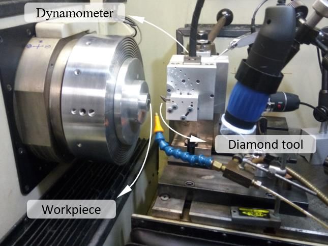
in the ductile-brittle response in the machining of semiconductor crystals. Thus, this study intends to evaluate the ductile-brittle response from the point of view of the area and the deformed volume in front of the tool when the rake angle becomes more negative. The aim is to have a response with continuity characteristics for the ductile response trend when the rake angle becomes more negative, along with variation in machining conditions. Furthermore, the anisotropy effect, resulting from the change in crystallographic direction, still needs to be quantified so that this deleterious effect can be avoided in the manufacture of optical components. 2 Material and Methods 2.1 Object of the study We used single crystal silicon in ultra-precision machining with a round nose diamond tool. The specimens (20 × 20 mm) were cut from silicon wafers with (100) surface orientation, 1 - 10 Ω.cm resistivity, P-type (Boron concentrations: 1015 - 1016 atoms cm−3), 55 mm diameter and 500 μm thick. Some physical and mechanical properties [38] are shown in Table 1. Cutting forces, surface finish, and the onset of uncut shoulder cracks propagation in machining are the main outputs assessed in this study. Table 1 – Properties of Single crystal silicon (100) [7, 38]. Material property Value Density (g/cm³) 2.328 Melting point (ºC) 1,420 Young modulus (GPa) (100) 131 Shear modulus (GPa) 79.9 1/2 Fracture toughness (MPa.m ) 0.95 Poisson’s ratio 0.266 Hardness load 10 g HVickers (GPa) 11.3 Single point diamond turning experiments were carried out on a commercially available diamond turning machine, the Aspheric Surface Generator Rank Pneumo ASG 2500. This is a very rigid system with T-base carriage configuration and carriages (hydrostatic bearing, driven with pulse-width-modulated dc servomotors, rotary-to-linear motion through 5 mm pitch ballscrews, and position feedback using laser interferometer) that had a 10 nm positioning accuracy.
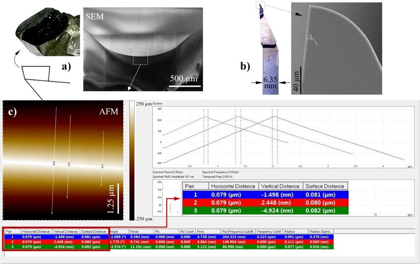
The commercial monocrystalline diamond tools used for the experiment have a nose
radius of 762 µm (Figure 2a) and 100 µm (Figure 2b), clearance angles of 10º, rake angles of
0º, and cutting edge radius of the order of 40 nm by measuring the cross sectional of the cutting
edge as shown in Figure 2c using atomic force microscope.

Figure 2 – Monocrystalline diamond tools with cutting edge radius of the order of 40 nm.
a) Nose radius Rε = 762 µm and α = 0º. b) Nose half-radius Rε = 100 µme α = 0º. c) Edge
radius = 40 nm. SEM: Scanning Electron Microscope; AFM: Atomic Force Microscopy.

2.2 Machining Experiment and Data Analysis

 The statistical technique applied to the machining experiment was the Central Composite
Design (CCD). This planning is a first order factorial increased by additional points to allow
the estimation of parameters of a second order surface. The method adopted here was that of
rotation proposed by Box et al. [39]. Two factors were analyzed: the tool feed ( ) and the tool
rake angle ( ).
 Table 2 presents the CCD’s statistical matrix for the execution of the machining
experiment. The lowest feedrate value for the statistical matrix was 2.5 µm/rev. For the tool's
rake angle, we chose to establish 0º as the lowest value of this statistical matrix. In order to
achieve the minimum point (-1.41) of the matrix, given by f = 2.5 µm/rev and α = 0º, we adopted
a central point (0) so that the points +1 and -1 varied by 1 µm/rev for feedrate f and 15º for rake
angle α. Thus, Equation 1, which determines the additional points (±1.41), provided the
desired minimum point ( 2.5µm/ 0º).

 (+1) − (−1)
 (±1.41) = (0) ± 1.41 ( ) (1)
 2
 Where is the value of f or α corresponding to the coding.

 The depth of cut (dc) was constantly kept at 10 µm. The constant speed rotation adopted
for the experiment was 1000 RPM, which provided mean values of cutting speed in the order
of 40 m/min: a low speed for machining in order to minimize the effect of heat.
 The order of execution of the points (samples) in the experiment was carried out at
random as shown in Table 2.

Table 2 – Experimental matrix of the central composite planning, with input factors the machining feed
rate (µm/revolution) and the tool rake angle (°).
 Central Composite Design Coded Factors Experiment**

 Coding Number*
 +1.41 5.5 -45° -1 -1 3.0 -7.5° 9
 +1 5.0 -37.5° -1 +1 3.0 -37.5° 7
 0 4.0 -22.5° +1 -1 5.0 -7.5° 10
 -1 3.0 -7.5° +1 +1 5.0 -37.5° 8
 -1.41 2.5 -0° -1.41 0 2.5 -22.5° 5
 +1.41 0 5.5 -22.5° 6
 0 -1.41 4.0 0° 1
 0 +1.41 4.0 -45.0° 2
 0 0 4.0 -22.5° 3
 0 0 4.0 -22.5° 4
 * The samples execution random order (tracks)
 ** Machining environment: wet cutting (Alkalisol 2050)
 ** Depth of cut (dc): 10 µm
 ** Spindle rotation rate: 1000 rpm

 Thus, machining tests were carried out on monocrystalline silicon samples randomly,
with a total of 10 machining conditions established based upon the central composite design
(Table 2). Feedrates ranged from 2.5 to 5.5 µm/rev at a depth of cut of 10 µm.
 As shown in Figure 3a, the first condition (track 1) is at the center of the experiment
and the last (track 10) is at the ultimate track. The schematic diagram of the step structure
generated by subsequent machining conditions from track 1 to 3 is illustrated by Figure 3b:
when machining the first track, the tool traveled across the entire surface, in the second track
it stopped beforehand so as not to eliminate track 1, and in track 3 also beforehand to not delete
track 2; thus, successively up until the ultimate track of the experiment. The width of the zone
generated by each condition is about 1 mm. Cutting fluid (Alkalisol 2050 - produced by Alkalis
Brasil) was applied for the machining in all zones.

 a) b)
 Figure 3 – Samples (tracks) of the machining experiment. a) Experiment finished
 (workpiece). b) Machining protocol for samples.

 The experimental setup is shown in Figure 4. This system consisted of a tool holder,
an angled base, and a dynamometer. The angular base was attached to the dynamometer and
the tool holder to the angular base in the position corresponding to the desired rake angles for
the experiment (Figure 4). The sample of silicon was fixed with heat-softening glue on a fixing
bracket, which was then fixed onto the vacuum chuck of the machine spindle (Figure 4). The
room temperature was 20 ºC during machining.

 Figure 4 – The experiment setup for rake angle variation and cutting force measurements.
2.2.1 Cutting Forces

 To measure the machining forces, an acquisition system was assembled, consisting of
an acquisition board (400 kHz), a multi-channel load amplifier, and a piezoelectric
dynamometer Kistler, model 9652C2 (0 to 250 N; natural frequency of 2 kHz), all commercial.
The forces were recorded at a sampling frequency of 130 kHz for each direction of force (x, y,
and z). The positioning of the dynamometer was established in such a way that the x-axis
provided the thrust force (Ft), the y-axis provided the cutting force (Fc), and the z-axis provided
the feed force (Ff).
 As shown in Figure 5, the thickness of cutting (h), depth of cut (dc), and the cutting
section area (As), are those corresponding to the layer to be removed, which is in front of the
tool. The effective thickness of cutting (ℎ ), the effective depth of cut ( ) and the effective
area of cutting section ( ) are those correlated with the tool inclination and will be influenced
by the rake angle (α).
 The transition pressure value (k N ) was determined by the decomposition of thrust and
cutting forces, distributed in the effective area of cutting section (As ), as expressed by
Equation (2).

Figure 5 - Material removal with negative rake angle: thickness of cutting (h) and effective
thickness of cutting (ℎ ); depth of cut (dc) and effective depth of cut ( ); cutting section area
(As) and effective area of cutting section ( ).

 N Fc cos α − Ft sen α
kN = = (2)
 Ase Ase

 f. dc
Ase = (3)
 cos|α|
 f: tool feedrate per revolution; dc: depth of cut; α: tool rake angle
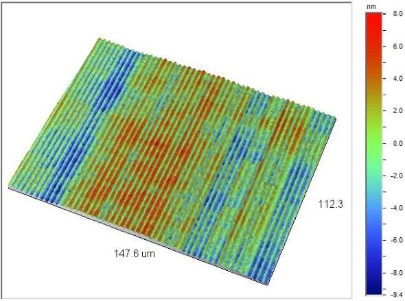
2.2.2 Surface Quality

 We measured cut surface finish using a VEECO non-contact high-resolution profiler
Wyko NT 1100. The parameter of areal surface roughness used was root-mean-square
roughness Rq. We carried out 6 measurements for each machining track: three measurements
in the direction [100] and three measurements in the direction [110] and then estimated an
average and standard deviation Rq for each cutting condition.

2.2.3 Uncut Shoulders and Critical Thickness of Cutting

 We used the Olympus LEXT OLS4100 laser scanning digital microscope non-contact
3D to analyze the uncut shoulders of each cut track (Figure 6), formed by the depth of cut (dc)
and the cutting radius (R c ) from machining experiment (Figure 3), Focusing using the
microscope on each uncut shoulder, it was possible to estimate the cutting radius by
measuring the printed shoulder after the tool is withdrawn.

 Figure 6 – Uncut shoulders of machining experiment.

 Nevertheless, the chip cross-sectional area generated in front of the tool rake face, when
the rake angle becomes more negative, forms a different curvature arc from that corresponding
to its nose radius (Rε). For example, when a 0º tool rake angle is used (Figure 7), the curvature
arc formed by the cutting radius (Rc) corresponds to the circumference arc on the tool nose
radius as schematically shown in Figure 7 (Rc = Rε). However, when the tool rake angle turns
negative (Figure 7), the curvature arc formed by the cutting radius acting on the rake face
becomes larger than the tool nose radius (Rc > Rε). This cutting radius Rc is increased
proportionally to the negative increase of α.
 The increase in the cutting radius is not entirely a circumference; its actual shape
resembles a parabola. However, when machining with a diamond tool, the tool nose radius is
much larger than the depth of cut, and the cutting radius can be estimated by a circumference.
Figure 7 – Increase in cutting radius R c as the rake angle becomes more negative.

 The onset of fractures is normally verified along the uncut shoulders [25]: the point
where the effective thickness of cutting he reaches its critical value (Figure 8: Fracture), and it
is called the critical-effective thickness of cutting (h∗e ). At this point, the material does not
support more deformations and the phase transition ceases. Since the critical depth of cut (dc ∗ )
of this fracture has been measured, the critical-effective thickness of cutting (h∗e ) can then be
determined by the tool feedrate (f), the tool rake angle (α), and the cutting radius (Rc), as
expressed by the equations in Figure 8.

Figure 8 – Uncut shoulder: determination of the critical-effective thickness of cutting. he∗ :
critical-effective thickness of cutting. dc ∗ : critical depth of cut. dc ∗ : critical-effective depth of
cut. R c : cutting radius.
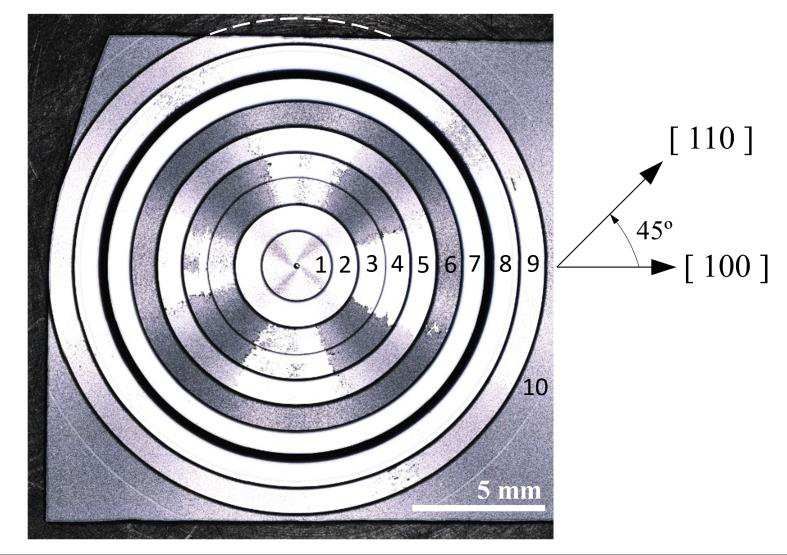
3 Results and discussion

 Using the statistical matrix, we obtained the response surfaces of the cutting transition
pressure and surface finish. The level curves of the transition pressure response surfaces
provided us with accurate mapping of the ductile-to-brittle transition region. Based on this
mapping, parameters for roughing operations were selected. The level curves of the surface
finish allowed us to determine the tool rake angle to obtain an optimum value of the surface
finish. In addition, we have advanced to the critical thickness of cutting as well. We generalized
its application to other tool nose radius sizes and different rake angles, taking into account the
influence of this angle on the nose radius contact area during chip formation. Thus, based upon
these results we ended the study with the manufacture of two Fresnel microlenses.

3.1 Machining Experiment

 Through the machining experiment, we determined the ductile machining region for a
specific tool nose radius (Re 762 µm). We also determined the best tool rake angle for finishing.
Furthermore, through this same experiment, we analyzed the uncut shoulders to generalize the
optimal material removal for any tool nose radius.
 Figure 9 presents a photograph showing a general view of the machined monocrystalline
silicon sample after cutting tests, with 10 tracks corresponding to each of the machining
conditions and rake angles, respectively as shown in Table 2. The crystallographic direction
[110] presented areas with darker shades than the direction [100] in the same track. This darker
shade represents damage caused by microcracks on the machined surface.

Figure 9 – Single crystal silicon (100) workpiece from machining experiment with a diamond
tool (Rε 762 µm). Track 1 in the center to Track 10 on the outmost region of the experiment.
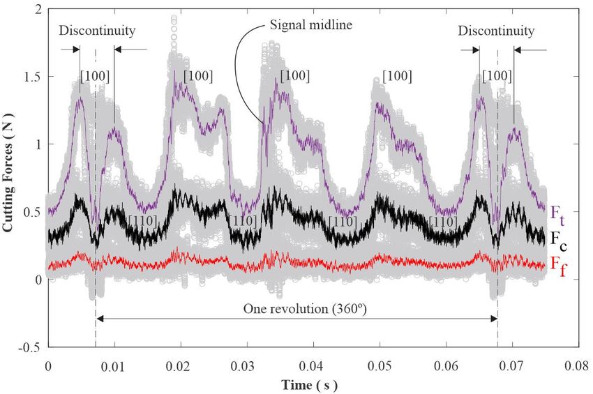
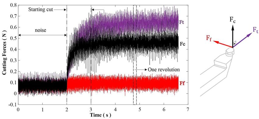
Figure 9 shows that the material removal took place predominantly in brittle mode within
tracks 6 and 10; ductile and brittle within tracks 1, 3, 4, and 5; and predominantly in ductile
mode within tracks 2, 7, and 8. Considering the direction where there is a predominance of the
brittle mode as [110] direction, it is important to mention that the direction [110] is the softest
direction on the crystallographic plane (100) [7]. This corroborates the results reported by
Mukaida and Yan [36], who performed turning on silicon (100) which also showed that the
brittle fracture occurs preferentially in the direction [110]. Jasinevicius and collaborators [37]
explained this converse material response considering two important pieces of information: the
first is that with direction [110] being the softest direction, its transition pressure will be smaller
as well (8-9 GPa) [40], and therefore the difference between hardness and transition pressure
(11-12.5 GPa) will always be broader in the direction [110] in comparison to [100] (12 GPa).
The second factor to be considered is that, in machining, the shear stress component is present
and lowers the transition pressure of the direction [100] by up to 40% [24, 41]. This turns it
more difficult for the direction [110] to reach the necessary pressure for the transformation
phase and instead of having a ductile response, we observe the fragile response.

3.1.1 Cutting Forces and Material Removal

 The cutting forces, in an overview plot, behaved as shown in Figure 10. Before machining,
we can observe the signal noise (noise). At the time of the tool-piece contact (Starting cut), the
machining forces began to increase and stabilized at a maximum value.

Figure 10 – Behavior of the machining forces of track 7 ( 3.0µm/α-37.5°) with diamond tool
(Rε 762 µm) on monocrystalline silicon (100). Ff: feed force, Ft: thrust force, Fc: cutting force.
Figure 10 shows cutting force behavior on track 9 during one revolution of the workpiece
where it is possible to observe the machining forces changing when the crystallographic
direction is changed. This track was chosen because the tool exits and re-enters the part, helping
to observe the interruption of the force signal and its resumption immediately after, as marked
with a dashed line in Figure 9. In this track, there was a discontinuity of machining in the
direction [100] and the forces tended to 0 at the point where the cut was interrupted. The values
of the machining forces for each machining track of the experiment are presented in Table 3:

Figure 11 – Machining forces of track 9 ( 3.0µm/ -7.5°) in the period of one revolution when
machining silicon (100) with a diamond tool (Rε 762 µm). Force decayed in one of the
directions [100] due to the cut discontinuity.

Table 3 – Average forces and standard deviation of the silicon machining experiment (100)
with a diamond tool (Rε 762 µm) at a machining depth of 10 µm.

 Experiment Fc [100] Fc [110] Ft [100] Ft [110]
 f (µm/rev) α (º) Track Mean Dev Mean Dev Mean Dev Mean Dev
 4.0 0° 1 0.715 0.026 0.585 0.012 0.828 0.083 0.470 0.036
 4.0 -45.0° 2 0.705 0.008 0.455 0.019 1.036 0.022 0.552 0.041
 4.0 -22.5° 3 0.565 0.097 0.183 0.008 1.057 0.208 0.132 0.008
 4.0 -22.5° 4 0.324 0.018 0.113 0.006 0.745 0.046 0.128 0.017
 2.5 -22.5° 5 0.512 0.002 0.191 0.003 1.239 0.012 0.403 0.001
 5.5 -22.5° 6 0.320 0.012 0.207 0.000 0.633 0.023 0.313 0.001
 3.0 -37.5° 7 0.512 0.028 0.420 0.013 0.688 0.046 0.482 0.038
 5.0 -37.5° 8 0.706 0.012 0.642 0.011 1.006 0.014 0.899 0.020
 3.0 -7.5° 9 0.536 0.032 0.271 0.013 1.220 0.105 0.426 0.048
 5.0 -7.5° 10 0.403 0.015 0.286 0.010 0.865 0.043 0.517 0.012
 *Dev: Standard Deviation
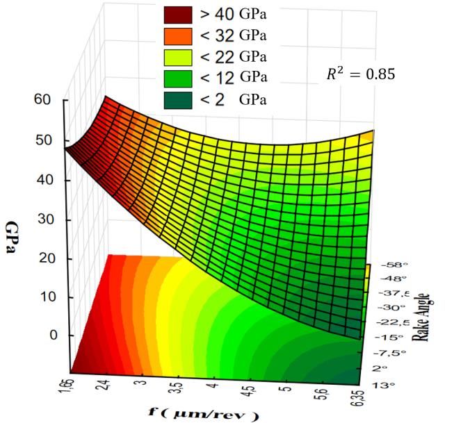
The statistical treatment of the central composite planning (CCD) of the Ft and Fc forces
(Table 3) distributed over the effective area of the cutting section of the tool, Equation (2),
provided the respective brittle-ductile transition pressures as shown in Figure 12.

 [ 100 ] [ 110 ]

 a) b)

 c) d)
Figure 12 – Response surfaces (a and b) and level curves (c and d) of the Transition Pressure
from the machining experiment with monocrystalline Silicon (100) with single point diamond
tool (Rε 762 µm). The numbers from 1 to 10 correspond to the values obtained in the respective
machining tracks.

 The determination of the brittle-to-ductile transition during machining was carried out by
comparing the pressure results generated in each machined track with the response surface
level curves. In the crystallographic direction [100], only tracks 6 and 10 underwent brittle
fractures on their surfaces (Figure 9). The band that passed above these tracks is the dash-point
curve (Figure 12c). The inner portion, delimited by the dash-point curve, defined the material
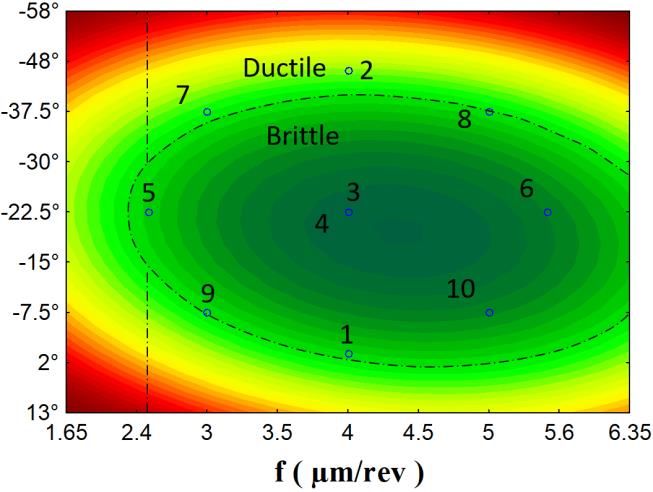
removal mode as predominantly brittle; and the outer portion: prominently ductile. The value
of this transition line for direction [100] is of a transition pressure around 12 GPa.
 The same criterion for determining the brittle-to-ductile transition was applied for
direction [110], only tracks 2 and 7 were predominantly ductile in this crystallographic
direction. However, track 8 presented itself as an intermediate point as two of the four
directions [110] have fractured (Figure 9). The band that passed below the point of track 7 and
above track 8, bounded by the dash-point ellipse (Figure 12d) determined the transition region
in that direction. All other bands that have suffered a fracture were found in the inner part of
this trace-point ellipse. The transition pressure value for this band, corresponding to the
direction [110], was approximately 13 GPa.
 The crystallographic direction [110] generated a smaller cutting force and thrust force in
comparison to the crystallographic direction [100] (Figure 11), corroborating the results
presented by O'Connor and collaborators [7]. In addition, this direction [110] demanded a
higher compression pressure (13 GPa) for phase transformation to take place and to shift from
brittle to ductile material removal mode. These two factors corroborate what was discussed
earlier.
 The contour lines of these two crystallographic directions were combined to map the shift
in transition pressure in both directions simultaneously (Figure 13). Thus, for a given feedrate
value there will be a critical angle corresponding to a ductile machining condition. This
mapping, therefore, allowed the selection of machining parameters for roughing operations. To
exemplify this statement, let's go back to Figure 13, for a feed rate greater than 4.5 µm/rev,
more negative rake angles around -37.5º would be indicated to achieve the material removal
free from damage caused by microcracks on the surface of the part. This improvement of
machining with a negative increase of the rake angle was also observed for other types of
crystals (Zinc Sulfide - ZnS) [42]. Although, for very long machining processes (30 - 60 km),
high negative rake angles can generate a higher rate of tool wear [43].
Figure 13 – Mapping of the ductile region of Silicon (100) from level curves shown in Figure
12c and Figure 12d, respectively, for roughing operations in machining with circular diamond
tool Rε 762 µm.

3.1.2 Surface Finish

 According to the machined surfaces state (Table 4), we observed that these surfaces
alternated between fractured (brittle mode) and crack-free (ductile mode). In the ductile
direction [100] only tracks 1 and 10 presented fractures. Conversely, only track 7 of the fragile
direction [110] was crack free. The roughness of these surfaces was measured using a profile.
An analysis of the effect of the average showed the significant difference in the finish (Rq) of
the surfaces obtained in the ductile mode (3- 8 nm) and the brittle mode (100 - 250 nm).

Table 4 – Surface State of the machined tracks cut with a diamond tool ( 0,762mm).
 [100] [110]
1 ( 4,0µm/ 0º)

 Ra 6.43 nm Rq 7.95 nm Rt 49.35 nm Ra 14.25 nm Rq 17.47 nm Rt 111.88 nm
2 ( 4,0µm/ -45°)

 Ra 3.33 nm Rq 4.09 nm Rt 22.33 nm Ra 10.36 nm Rq 12.68 nm Rt 74.60 nm
3 ( 4,0µm/ -22,5°)

 Ra 3.82 nm Rq 4.68 nm Rt 26.37 nm Ra 123.16 nm Rq 160.06 nm Rt 1200 nm
4 ( 4,0µm/ -22,5°)

 Ra 2.52 nm Rq 3.14 nm Rt 20.44 nm Ra 139.46 nm Rq 185.50 nm Rt 1350 nm
5 ( 2,5µm/ -22,5°)

 Ra 3.04 nm Rq 3.75 nm Rt 19.59 nm Ra 70.43 nm Rq 98.36 nm Rt 742.71 nm
6 ( 5,5µm/ -22,5°)

 Ra 150.70 nm Rq 202.45 nm Rt 1440 nm Ra 178.53 nm Rq 237.73 nm Rt 1760 nm
7 ( 3,0µm/ -37,5°)

 Ra 3.46 nm Rq 4.21 nm Rt 21.79 nm Ra 2.61 nm Rq 3.20 nm Rt 17.40 nm
8 ( 5,0µm/ -37,5°)

 Ra 3.71 nm Rq 4.62 nm Rt 26.04 nm Ra 3.60 nm Rq 4.57 nm Rt 26.82 nm
9 ( 3,0µm/ -7,5°)

 Ra 5.17 nm Rq 6.35 nm Rt 37.80 nm Ra 91.57 nm Rq 140.11 nm Rt 1590 nm
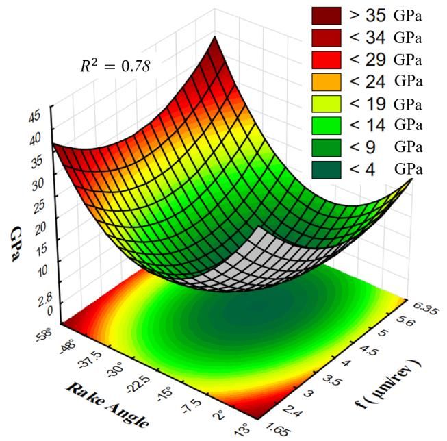
10 ( 5,0µm/ -7,5°)

 Ra 67.51 nm Rq 94.78 nm Rt 751.20 Ra 128.60 nm Rq 187.63 nm Rt 1490 nm

 From the measurements of root-mean-square surface roughness (Rq) of the machined
surfaces (Table 4), we generated the response surfaces of the CCD’s statistical treatment. The
level curves of these response surfaces are shown in Figure 14. The regions of optical finish
(Rq ≤ 15 nm) are demarcated within the trace-point band. In the crystallographic direction
[100] can be obtained optical finish with a high feedrate of 5 µm/rev coupled with a very
negative rake angle (-45 °). This behavior also occurred for all combinations of feedrates and
rake angles that were within the limit band (dash-point line). However, these limit bands
became narrow in the crystallographic direction [110].
 To achieve the same order of magnitude in the optical finish in the direction [110],
feedrates from 2.5 to 5.5 µm/rev needed to work in conjunction with rake angles around -37.5°.
Furthermore, based upon this it would be an appropriate choice for a feedrate and rake angle
condition that best meets the crystallographic direction [110], which would therefore fully meet
the crystallographic direction [100]. In this case, the recommended rake angle was around
- 37.5º for the best surface finish.

 [ 100 ] [ 110 ]

Figure 14 – Level curves of the Rq (nm) surface roughness of the machining experiment of
silicon (100) with single point diamond tool (Rε 762 µm).
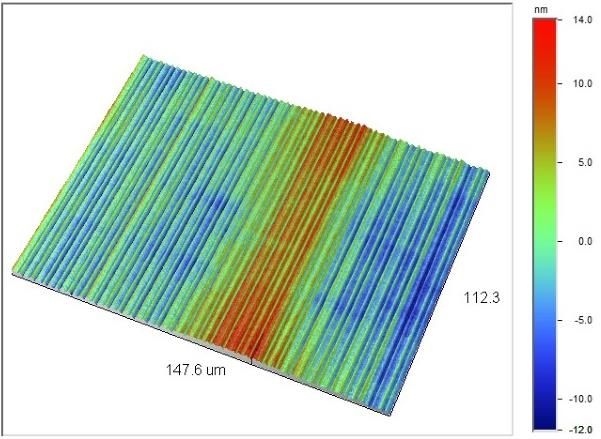
3.1.3 Uncut shoulders

 The analysis of the brittle-to-ductile transition carried out on the uncut shoulder allowed
the determination of the critical depth of cut (dc*) corresponding to that where the cracks
stopped propagating (Figure 15).

Figure 15 – One of the uncut shoulder measurements from experiment track 8 (f5.0μm/ -
37.5°) generated by a diamond tool (Rε 762 μm): Rc = 1100 µm; and dc* = 6.5 µm.

 The cutting radii measured in each of the machined tracks are shown in Figure 16. We
chose to keep an equation that governs the characteristic curve of the variation of the cutting
radius as a function of the rake angle based on three-dimensional drawings (Equation 4), to
exactly match the values of the rake angles used. It was observed that the values adjusted by
Equation 4 were close to the experimental values (Figure 16). On average, there was a 5%
difference between the calculated cutting radii and the cutting radii of the machining
experiment. This difference can be related to fractured surfaces.

 Figure 16 – Cutting radius from as a function of the rake angle.
R c = R ε (1.0078 − 3.065. |α|1.804 . 10−4 )−1 µm dc ≤ 0.1R ε 4

 Since determining cutting radius (Rc), the critical-effective depth of cut (dce *) was then
calculated so that, according to the equations in Figure 8, it was possible to determine the
critical-effective thickness of cutting (he*) of silicon as a function of the tool rake angle (Figure
17). Using this procedure, we calculated for the crystallographic direction [100], with a tool's
rake angle variation from 0º to -45º, the values of critical-effective thickness of cutting, which
varied from 250 nm to 550 nm.
 Yan and collaborators [44] using nanoprecision plunge cut tests on silicon (100), measured
the thickness of cutting versus tool rake angle variation between -15º and -45º. The authors
found that in direction [100] there was a variation in the critical thickness of cutting between
50 nm and 500 nm, and the increase in critical thickness was directly proportional to the
negative rake angle [33].
 Regarding the direction [110], our estimate of the critical-effective thickness of cutting
was only possible on track 7, all other tracks showed microcrack along all uncut shoulder width
and propagated to the finished surface. Comparing the critical thickness of cutting from track
7 in both directions [110] and [100], we found that he* [110] corresponds to 35% of he* [100].
This reduction in the critical thickness of cutting in the direction [110] was observed by Yan
and collaborators [44]. Similarly, O’Connor, Marsh, and Couey [45] concluded that the ratio
between the critical thickness of cutting for [110] and [100] direction was 33%.

 Figure 17 – Critical-effective thickness of cutting of monocrystalline silicon (100).
In addition to the critical thickness of cutting, we estimated the value of the critical depth
of cut (dc*), at which the cracks propagated, but did not reach the cut surface line [46]. Such
depth must be greater than 3 µm for direction [100]. As shown in Figure 9, this value was found
from tracks 3 and 4, three of the four directions [100] of these tracks showed slight fractures
on the surface: he* is likely to be at the limit of its critical depth. On the other hand, for direction
[110] the critical depth of he*[110] must be greater than 10 µm. This assumption is based on
track 8, this track presented superficial fractures in two of the four directions [110]. Thus, we
found that dc*[110] corresponds to 3.35 times dc*[100]; that is, in machining the cracks that
propagate in the direction [110] reach greater lengths.
 Therefore, as mentioned above and according to Figure 17, in relation to the direction
[110], the critical-effective thickness of cutting (nm) and its critical depth of cut (µm) can be
determined by:

h∗e110 = 2.6α + 78 nm 5
 ∗
dc110 > 10 µm 6
 α in absolute values

3.2 Application

After determining the limits of the critical depth of cut and the critical-effective thickness of
cutting, we decided to apply these results to manufacture a diffractive optical element (DOE’s).
For this, two Fresnel microlenses with concave and convex profiles, diameter of 3 mm, 11
zones with a height of 7 µm, were machined in Si (100) (Figure 18). Based on our analysis we
chose a rake angle of -37.5º seeking a better finishing response in the direction [110] (Figure
14). First, it was necessary to carry out a roughing step on the surface. We adjusted the device
at this angle for the roughing operation. For roughing operation, we based on the mapping in
Figure 13. We used the same depth of cut as the experiment (dc = 10 µm) and a diamond tool
with the same nose radius (Rε = 762 µm). As shown in Figure 13, to achieve ductile material
removal with a tool rake angle of -37.5º, the maximum possible tool feed rate is 3 µm/rev.

3.2.1 Fresnel Lenses

 In the manufacturing of the Fresnel lenses, we used a half-radius diamond tool Rε =
100 µm (Figure 2). With a rake angle positioned at -37.5º, the critical-effective thickness of
cutting is around 175 nm in the [110] direction (Equation 5).
We could have made two decisions here: case 1 - would be to work within this limit of the
critical-effective thickness of cutting, he*[110] = 175 nm, and to set up he*[110] to a height
corresponding to your critical depth [25]. The other, case 2, would be to work with a maximum-
effective thickness of cutting always smaller than the critical-effective thickness of cutting. We
then chose to work the second option.
To determine the tool feedrate, we used the common mathematical relationships of the
maximum-effective thickness of cutting for tools with nose radius and took the critical-
effective thickness of cutting, from direction [110], as a basis (Equation 5). Thus, for ductile
machining of Si (100) with a round tip diamond tool, the tool feedrate (µm/rev) can be
determined by the expression of Equation 7.
(2.6α + 78). 10−3 1
= µm/rev 7
sin{ arccos[1 − dc (R c cos )−1 ] } C
C: safety factor ≥ 1
α in absolute values
dc can be substituted for dc* for case 1
Thus, using Equation 7 for a tool with a tip radius Rε = 100 µm (cutting radius Rc =
125 µm according to Equation 4) applied to a cutting depth of 7 µm (height of the Fresnel lens),
rake angle α = -37.5º (optimal finish), and considering a safety factor C = 2; the tool feedrate
(f) for ductile machining is in the order of 0.25 µm/rev. The maximum thickness of cutting for
this feedrate is 100 nm, which is less than the critical-effective thickness of cutting (175 nm)
of the direction [110].
This value of feedrate (0.250 m/rev) favored the achievement of finishing in the curved
areas of the Fresnel lenses (Figure 18). All curved surfaces in the lens areas were free of brittle
damages. This demonstrated the ability to apply the critical-effective thickness of cutting value
for different rake angles and tool nose radii. This is since these thicknesses of cutting are
related to the cutting radius (Rc) during machining; thus, providing the critical-effective
thickness of cutting.a) b) Figure 18 – Fresnel lens manufactured with a half-radius diamond tool (Rε = 100 µm), = 0.25 µm/rev, α = -37.5º and dc = 7 µm. a) convex; b) concave. Nevertheless, we observed a certain fracture in the vertical walls of Fresnel lenses in the tool's plunge movement. This could probably be due to a fracture at the tip of the tool as shown in Figure 19. Since the tool performs a rotation movement together with the tool holder to reach a certain rake angle. Consequently, the clearance angle also followed in the same sense, decreasing the stiffness of the tool tip. To solve this issue, diamond tools with a -37.5º rake angle should be manufactured with a 10º clearance angle. Figure 19 – Diamond tool tip (Rε 100 µm) after machining of Fresnel lenses.
4 Conclusions

 In this study, we characterized the transition pressure, surface finish, and critical thickness
of cutting by the experimental-statistical analysis of ultra-precision machining of single-crystal
silicon (100) with a rounded-nose diamond tool, varying tool rake angle and feedrates.
 The mapping of the response surfaces, extracted from the statistical matrix of the brittle-
to-ductile transition pressure of the material (estimated to be 12 GPa for the direction [100] and
13 GPa for the direction [110] on silicon), enables determining the roughing parameters of the
machining in ductile mode: high feedrate with the appropriate rake angle.
 The mapping of the surface finish response surfaces, also through the statistical matrix,
enables determining the tool rake angle for the optimal machining finish. This angle is around
-37.5º for silicon (100).
 Besides the differences reported in the literature on the critical thickness of cutting between
directions [110] and [100], we also found differences in the lengths that cracks travel in each
direction, which reached greater lengths (around 3.35 times) in direction [110].
 Finally, we conclude that there is an intrinsic correlation between the critical thickness of
cutting, the tool rake angle, and the cutting radius during machining. These three factors should
be considered to allow the deterministic generalization of the optimal machining parameters.
Declarations

Funding: The experiment has been performed in the Precision Engineering Laboratory (PEL)
at the Department of Mechanical Engineering, School of Engineering of São Carlos, University
of São Paulo, Brazil. The study was supported by Federal Institute of Education, Science and
Technology of São Paulo (IFSP), and Brazilian grants from São Paulo Research Foundation
(FAPESP), Education Ministry Foundation (CAPES), and National Council for Scientific and
Technological Development (CNPq).

Conflicts of interest: The authors declare that they have no known competing financial
interests or personal relationships that could have appeared to influence the work reported in
this paper.

Availability of data and material: The data sets generated and analyzed from the current
study are available upon request from the corresponding author.

Code availability: The software application developed for the analysis of cutting forces is
available on request from the corresponding author.

Ethics approval, Consent to participate, and Consent for publication: Not applicable.

Authors' contributions: Marcel Henrique Militão Dib: Conceptualization, Investigation,
Methodology, Data Curation, Formal analysis, Software for Cutting forces, Writing - Original
Draft, Visualization, Validation. José Antonio Otoboni: Methodology, Validation, Writing -
Review & Editing. Renato Goulart Jasinevicius: Supervision, Conceptualization,
Methodology, Resources, Validation, Investigation, Data Curation, Writing - Review &
Editing.
REFERENCES

1. Abdulkadir LN, Abou-El-Hossein K, Jumare AI, et al (2018) Review of molecular
 dynamics/experimental study of diamond-silicon behavior in nanoscale machining. Int J
 Adv Manuf Technol 98:317–371. https://doi.org/10.1007/s00170-018-2041-7

2. Langfelder G, Bestetti M, Gadola M (2021) Silicon MEMS inertial sensors evolution over
 a quarter century. J Micromechanics Microengineering 31:084002.
 https://doi.org/10.1088/1361-6439/ac0fbf

3. Olufayo OA, Abou-El-Hossein K (2013) Molecular Dynamics Modeling of Nanoscale
 Machining of Silicon. Procedia CIRP 8:504–509.
 https://doi.org/10.1016/j.procir.2013.06.141

4. Budnitzki M, Kuna M (2016) Stress induced phase transitions in silicon. J Mech Phys
 Solids 95:64–91. https://doi.org/10.1016/j.jmps.2016.03.017

5. Gilman JJ (1992) Insulator-metal transitions at microindentations. J Mater Res 7:535–
 538. https://doi.org/10.1557/JMR.1992.0535

6. Domnich V, Gogotsi Y (2001) Pressure-Induced Phase Transformations In
 Semiconductors Under Contact Loading. In: Hochheimer HD, Kuchta B, Dorhout PK,
 Yarger JL (eds) Frontiers of High Pressure Research II: Application of High Pressure to
 Low-Dimensional Novel Electronic Materials. Springer Netherlands, Dordrecht, pp 291–
 302

7. O’Connor BP, Marsh ER, Couey JA (2005) On the effect of crystallographic orientation
 on ductile material removal in silicon. Precis Eng 29:124–132.
 https://doi.org/10.1016/j.precisioneng.2004.05.004

8. Morris JC, Callahan DL (1994) Origins of microplasticity in low-load scratching of
 silicon. J Mater Res 9:2907–2913. https://doi.org/10.1557/JMR.1994.2907

9. Morris JC, Callahan DL, Kulik J, et al (1995) Origins of the Ductile Regime in Single-
 Point Diamond Turning of Semiconductors. J Am Ceram Soc 78:2015–2020.
 https://doi.org/10.1111/j.1151-2916.1995.tb08612.x

10. Kunz RR, Clark HR, Nitishin PM, et al (1996) High resolution studies of crystalline
 damage induced by lapping and single-point diamond machining of Si(100). J Mater Res
 11:1228–1237. https://doi.org/10.1557/JMR.1996.0157

11. Tanikella BV, Somasekhar AH, Sowers AT, et al (1996) Phase transformations during
 microcutting tests on silicon. Appl Phys Lett 69:2870–2872.
 https://doi.org/10.1063/1.117346

12. Pizani PS, Jasinevicius R, Duduch JG, Porto AJV (1999) Ductile and brittle modes in
 single-point-diamond-turning of silicon probed by Raman scattering. J Mater Sci Lett
 18:1185–1187. https://doi.org/10.1023/A:1006694310171

13. Jamieson JC (1963) Crystal Structures at High Pressures of Metallic Modifications of
 Silicon and Germanium. Science

14. Jayaraman A, Klement W, Kennedy GC (1963) Melting and Polymorphism at High
 Pressures in Some Group IV Elements and III-V Compounds with the
 Diamond/Zincblende Structure. Phys Rev 130:540–547.
 https://doi.org/10.1103/PhysRev.130.540
15. Bundy FP (1964) Phase Diagrams of Silicon and Germanium to 200 kbar, 1000°C. J
 Chem Phys 41:3809–3814. https://doi.org/10.1063/1.1725818

16. Minomura S, Drickamer HG (1962) Pressure induced phase transitions in silicon,
 germanium and some III–V compounds. J Phys Chem Solids 23:451–456.
 https://doi.org/10.1016/0022-3697(62)90085-9

17. R. H. Wentorf J, Kasper JS (1963) Two New Forms of Silicon. Science

18. Hull R, Institution of Electrical Engineers (1999) Properties of crystalline silicon.
 INSPEC, London

19. Hu JZ, Merkle LD, Menoni CS, Spain IL (1986) Crystal data for high-pressure phases of
 silicon. Phys Rev B 34:4679–4684. https://doi.org/10.1103/PhysRevB.34.4679

20. Gogotsi Y, Rosenberg MS, Kailer A, Nickel KG (1998) Phase Transformations in
 Semiconductors Under Contact Loading. In: Bhushan B (ed) Tribology Issues and
 Opportunities in MEMS. Springer Netherlands, Dordrecht, pp 431–442

21. Pharr GM, Oliver WC, Harding DS (1991) New evidence for a pressure-induced phase
 transformation during the indentation of silicon. J Mater Res 6:1129–1130.
 https://doi.org/10.1557/JMR.1991.1129

22. Cai MB, Li XP, Rahman M (2007) High-pressure phase transformation as the mechanism
 of ductile chip formation in nanoscale cutting of silicon wafer. Proc Inst Mech Eng Part
 B J Eng Manuf 221:1511–1519. https://doi.org/10.1243/09544054JEM901

23. Clarke DR, Kroll MC, Kirchner PD, et al (1988) Amorphization and Conductivity of
 Silicon and Germanium Induced by Indentation. Phys Rev Lett 60:2156–2159.
 https://doi.org/10.1103/PhysRevLett.60.2156

24. Gupta MC, Ruoff AL (1980) Static compression of silicon in the [100] and in the [111]
 directions. J Appl Phys 51:1072–1075. https://doi.org/10.1063/1.327714

25. Blake PN, Scattergood RO (1990) Ductile-Regime Machining of Germanium and Silicon.
 J Am Ceram Soc 73:949–957. https://doi.org/10.1111/j.1151-2916.1990.tb05142.x

26. Gilman JJ (1993) Shear-induced metallization. Philos Mag B 67:207–214.
 https://doi.org/10.1080/13642819308207868

27. Xiao GB, To S, Jelenković EV (2015) Effects of non-amorphizing hydrogen ion
 implantation on anisotropy in micro cutting of silicon. J Mater Process Technol 225:439–
 450. https://doi.org/10.1016/j.jmatprotec.2015.06.017

28. Yan J, Asami T, Harada H, Kuriyagawa T (2009) Fundamental investigation of
 subsurface damage in single crystalline silicon caused by diamond machining. Precis Eng
 33:378–386. https://doi.org/10.1016/j.precisioneng.2008.10.008

29. Scattergood RO, Blake PN (1989) Ductile-regime turning of germanium and silicon

30. Jasinevicius RG, Pizani PS, Duduch JG (2000) Brittle to ductile transition dependence
 upon the transition pressure value of semiconductors in micromachining. J Mater Res
 15:1688–1692. https://doi.org/10.1557/JMR.2000.0243
31. Blackley WS, Scattergood RO (1991) Ductile-regime machining model for diamond
 turning of brittle materials. Precis Eng 13:95–103. https://doi.org/10.1016/0141-
 6359(91)90500-I

32. Tanaka H, Shimada S, Anthony L (2007) Requirements for Ductile-mode Machining
 Based on Deformation Analysis of Mono-crystalline Silicon by Molecular Dynamics
 Simulation. CIRP Ann 56:53–56. https://doi.org/10.1016/j.cirp.2007.05.015

33. Venkatachalam S, Li X, Liang SY (2009) Predictive modeling of transition undeformed
 chip thickness in ductile-regime micro-machining of single crystal brittle materials. J
 Mater Process Technol 209:3306–3319. https://doi.org/10.1016/j.jmatprotec.2008.07.036

34. Yu B, Qian L (2013) Effect of crystal plane orientation on the friction-induced
 nanofabrication on monocrystalline silicon. 8

35. Blackley WS, Scattergood RO (1990) Crystal Orientation Dependence of Machning
 Damage-A Stress Model. J Am Ceram Soc 73:3113–3115.
 https://doi.org/10.1111/j.1151-2916.1990.tb06730.x

36. Mukaida M, Yan J (2017) Ductile machining of single-crystal silicon for microlens arrays
 by ultraprecision diamond turning using a slow tool servo. Int J Mach Tools Manuf 115:2–
 14. https://doi.org/10.1016/j.ijmachtools.2016.11.004

37. Jasinevicius RG, Duduch JG, Montanari L, Pizani PS (2012) Dependence of brittle-to-
 ductile transition on crystallographic direction in diamond turning of single-crystal
 silicon. Proc Inst Mech Eng Part B J Eng Manuf 226:445–458.
 https://doi.org/10.1177/0954405411421108

38. Jasinevicius RG, Pizani PS (2007) Annealing treatment of amorphous silicon generated
 by single point diamond turning. Int J Adv Manuf Technol 34:680–688.
 https://doi.org/10.1007/s00170-006-0650-z

39. Box GEP, Hunter JS, Hunter WG (2005) Statistics for Experimenters: Design, Innovation,
 and Discovery. Wiley

40. Jasinevicius RG, Duduch JG, Pizani PS (2008) The influence of crystallographic
 orientation on the generation of multiple structural phases generation in Silicon by cyclic
 microindentation. Mater Lett 62:812–815. https://doi.org/10.1016/j.matlet.2007.06.071

41. Gerbig YB, Stranick SJ, Morris DJ, et al (2009) Effect of crystallographic orientation on
 phase transformations during indentation of silicon. J Mater Res 24:1172–1183.
 https://doi.org/10.1557/jmr.2009.0122

42. Zong WJ, Cao ZM, He CL, Xue CX (2016) Theoretical modelling and FE simulation on
 the oblique diamond turning of ZnS crystal. Int J Mach Tools Manuf 100:55–71.
 https://doi.org/10.1016/j.ijmachtools.2015.10.002

43. Mir A, Luo X, Cheng K, Cox A (2018) Investigation of influence of tool rake angle in
 single point diamond turning of silicon. Int J Adv Manuf Technol 94:2343–2355.
 https://doi.org/10.1007/s00170-017-1021-7

44. Yan J, Asami T, Harada H, Kuriyagawa T (2012) Crystallographic effect on subsurface
 damage formation in silicon microcutting. CIRP Ann 61:131–134.
 https://doi.org/10.1016/j.cirp.2012.03.070
45. O’Connor BP, Marsh ER, Couey JA (2005) On the effect of crystallographic orientation
 on ductile material removal in silicon. Precis Eng 29:124–132.
 https://doi.org/10.1016/j.precisioneng.2004.05.004

46. Blake PN, Scattergood RO (1990) Ductile-Regime Machining of Germanium and Silicon.
 J Am Ceram Soc 73:949–957. https://doi.org/10.1111/j.1151-2916.1990.tb05142.x
You can also read