Low dephasing and robust micromagnet designs for silicon spin qubits
←
→
Page content transcription
If your browser does not render page correctly, please read the page content below
Low dephasing and robust micromagnet designs for silicon spin qubits
N. I. Dumoulin Stuyck,1, 2 F. A. Mohiyaddin,2 R. Li,2 M. Heyns,1, 2 B. Govoreanu,2 and I. P. Radu2
1) Department of Materials Engineering (MTM), KU Leuven, B-3001 Leuven, Belgium
2) imec, B-3001 Leuven, Belgium
(*Electronic mail: roy.li@imec.be)
(Dated: 25 August 2021)
Using micromagnets to enable electron spin manipulation in silicon qubits has emerged as a very popular method,
enabling single-qubit gate fidelities larger than 99.9%. However, these micromagnets also apply stray magnetic field
gradients onto the qubits, making the spin states susceptible to electric field noise and limiting their coherence times.
arXiv:2108.10769v1 [cond-mat.mes-hall] 24 Aug 2021
We describe here a magnet design that minimizes qubit dephasing, while allowing for fast qubit control and address-
ability. Specifically, we design and optimize magnet dimensions and position relative to the quantum dots, minimizing
dephasing from magnetic field gradients. The micromagnet-induced dephasing rates with this design are up to 3-orders
of magnitude lower than state-of-the-art implementations, allowing for long coherence times. This design is robust
against fabrication errors, and can be combined with a wide variety of silicon qubit device geometries, thereby allowing
exploration of coherence limiting factors and novel upscaling approaches.
Silicon quantum dot-based spin qubit systems have
demonstrated attractive properties for quantum computation,
including long qubit coherence times and high-fidelity single-
and two-qubit gates1–5 . The introduction of patterned on-chip
micromagnets has allowed high-speed and full electrical
spin manipulation using Electric Dipole Spin Resonance
(EDSR)6–15 , and enabled > 99.9% single-qubit gate fi-
delity so far3 . Furthermore, micromagnets have sparked
novel physical mechanisms for spin control, read-out and
manipulation16,17 . However, the micromagnet generated
gradients are a double-edged sword, as detrimental magnetic
field gradients in combination with electric field noise result in
substantial dephasing of the qubit. Indeed, successful demon-
strations of EDSR with spin qubits have reported charge
noise as the limiting factor for longer qubit coherence times
and higher spin control fidelities3,12,13 . The open challenge is
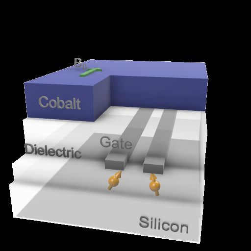
to minimize the qubit dephasing rate while still allowing fast FIG. 1. a) Design of the micromagnet. The x-y-z coordinate axis
manipulation and qubit addressability in larger-scale arrays. denotes the relative position of the micromagnet to the gate defined
In this Letter, we present optimized micromagnet designs quantum dots, shown in b). For simplicity, only two quantum dots are
that address this challenge and facilitate both low qubit shown but this number can be extended to a larger array. A magne-
dephasing and fast control, as well as ensure individual qubit tizing field B0 is applied along the y-direction and splits the confined
addressability for large quantum dot array implementations. electron’s spin states. c) Magnetic field difference along the quan-
In comparison to previous works, which mainly focused tum dot placements (x-direction) which allows for qubit addressabil-
dy
on qubit manipulation speed and addressability18–20 , here ity. d) Maximum of dephasing gradients bdeph and bdx deph . e) coupling
we use multiphysics based modelling that correlate design field gradient generated by the magnets. Fields are simulated for a
parameters to the qubit performance, and co-optimize the 600 nm gap design and taken at dQDM = 120 nm. Dashed circles de-
dephasing field gradients. The presented design and insight note typical quantum dot locations, horizontal dashed lines show the
micromagnet outline.
can be readily and widely implemented in popular Si-MOS
and Si/SiGe based spin qubit architectures. By resolving
the micromagnet induced dephasing, the design will allow
further exploration of coherence-limiting factors, crucial for field gradients that is robust against misplacement errors
the development of large-scale spin qubit arrays21,22 . due to fabrication. We show that, at this optimal point,
low dephasing can be achieved while maintaining fast qubit
The remainder of the paper is organised as follows. We manipulation speeds and qubit addressability. Finally, we
start by introducing a popular micromagnet topology along estimate expected micromagnet-induced dephasing rates and
with its relevant design parameters, while stressing that coherence times in the presence of charge noise, highlighting
the optimization is extendable to other micromagnet device an improvement by over three orders of magnitude in our
topologies. We show the typical magnetic fields and their optimized design.
gradients that can be expected from the design. Next, we The qubit states are encoded in the spin states of an elec-
demonstrate an optimal design point with minimal dephasing tron confined in a gated nanostructure23 , as shown in Fig. 1(b).
Spin manipulation via EDSR is performed by displacing the2
electron wavefunction through gate generated electric fields in between neighbouring qubits and allows for qubit addressabil-
magnetic field gradients, locally generated by micromagnets. ity, where we assume an experimentally achievable and com-
The micromagnet design is shown in Fig. 1(a), as well as its monly used quantum dot pitch of 100 nm1,3,5,10 . For optimal
relevant dimensions, design parameters and chosen axis ori- operation, bdeph should be low to minimize dephasing, bcoup
gin. For typical EDSR experiments, qubits are placed in the should be high for fast spin operations, and γe ∆By /h should
center of the gap along the x-direction to achieve high manipu- be at least 10× larger than the qubit EDSR linewidth for ad-
lation speed and addressability18 . We study the magnetization dressability, where h is Planck’s constant. 2D-linecuts for an
of the magnet and the resulting 3D magnetic fields by solving optimized design are shown in Fig. 1, taken at a quantum dot-
the Landau-Lifshitz-Gilbert equation numerically24,25 , and we to-micromagnet separation (dQDM ) of 120 nm.
refer to the supplementary material for all spatial compo- dy
The variation of bdeph as a function of dQDM , shown in
nents and gradients of the magnetic field. We chose a nu- dy
merical approach to be able to accurately determine the mag- Fig. 2(a), reveals an optimal dQDM where bdeph is minimized.
dy
netic fields for non-regular micromagnets, which might not be The origin of the minimal bdeph is illustrated in Fig. 2(b).
fully magnetized at smaller magnetic fields. Here, we chose The micromagnet components on each side of the gap gen-
Cobalt as the micromagnet material because of its strong dy
erate two bdeph that have opposite signs over the central re-
ferromagnetism and widespread use in spin-based quantum gion and hence cancel out. For an optimal dQDM , the to-
computation7–10,12,16–18,26 . Furthermore, we focus on a mag- dy
net thicknesses of 200 nm as it is a commonly used value, and tal bdeph is almost zero over an extended area, in both x-
has a relatively weak influence on the magnetic fields. For and y-directions. Although bdx deph has no minimum as func-
the external applied magnetic field, typical values are in the tion of dQDM , Fig. 2(c) shows that there exists a sweetspot
range of a few 100 mT to ∼1 T7–10,12,18 . We studied the ef- along the x-direction where bdx deph can be minimized. Even-
fect of this external field on the magnetization and found the tually, the qubit dephasing rate is determined by the direc-
micromagnet optimization depends only weakly on magneti- tion of the wavefunction displacement due to charge noise
zation fields changing between 100 mT and 10 T (see supple- which depends on the details of the device confinement po-
mentary material for details). We use a B0 of 0.7 T along the tential and electrical environment. Fig. 2(d) shows that the
y-direction in the following results and discussions, and refer dephasing gradient is minimized for displacements along the
the reader to the supplementary material for the full system dy-direction. As shown in Fig. 1(c) and Fig. 2(a) the low-
Hamiltonian. In this architecture, the qubit’s coherent two- dephasing area extends up to a few 100 nm in the qubit plane
level system is formed by the electron spin up and down state, and ∼ 30 nm in the z-direction. At this optimized depth, qubits
which are split in energy by the external applied magnetic field placed within this area will be highly robust against dephasing
B0 and micromagnet field By along the y-direction. This en- arising from charge noise.
ergy splitting is given by the Zeeman energy EZ = γe B0 , where So far, we have considered the case where the micromagnet
γe ≈ 116 µeV/T is the electron gyromagnetic ratio. To identify gap size is 600 nm. We find for all gap sizes between 300 nm
optimal magnet dimensions, we define the following parame- dy
and 1 µm there exists an optimal dQDM , where bdeph is mini-
ters: mal as shown in Fig. 3(a). Furthermore, Fig. 3(b) shows that
dx,dy dBy for each gap size, sufficiently high spin manipulation speed
bdeph (x, y) = max (X,Y ) and qubit addressability can be achieved at their respective
X,Y ∈A(x,y) dx, dy
s optimal dQDM . Using the middle point as an example,when
2 2
the gap is 600 nm, bcoup ∼ 0.5 mT/nm and ∆By > 5 mT. Ap-
dB x dB z
bcoup (x, y) = min (X,Y ) + (X,Y ) plying an electron displacement amplitude δ rd ≈ 1 nm during
X,Y ∈A(x,y) dy dy
EDSR10 , we can derive a Rabi frequency of γe bcoup δ rd /2h ≈
∆By (x, y) = By (x − 50 nm, y) − By (x + 50 nm, y) , 7 MHz. The EDSR resonance frequency difference between
qubits is given by ∆ f0 = γe ∆By /h ≈ 140 MHz, which allows
high frequency addressability with little crosstalk.
with A(x, y) defined as the quantum dot footprint of 50 × Previous experimental EDSR demonstrations3,9,10,18 made
50 nm2 , centred around (x, y). Taking the maximum of bdeph use of a micromagnet design with a gap of ∼ 300 nm and a
and minimum of bcoup over A(x, y) ensures the worst-case sce- sub-optimal dQDM ∼ 250 nm, and indeed reported dephasing
nario in electron wavefunction distribution, taking into ac- times limited by the detrimental micromagnet gradients and
count the quantum dot position uncertainty due to fabrica- presence of charge noise3,12,13 . To quantify the importance of
tion tolerances and stray electric fields. Here, the gradients a low dephasing field we can relate bdeph to the qubit coher-
dx,dy
bdeph are directed parallel to the external applied magnetic ence time T2∗ :
field B0 and, in the presence of charge noise, causes dephas- √
ing of the qubit7 . dBy /dz is negligible since the electron h ln 2
T2∗ =
wavefunction is strongly confined at the interface, and it is πγe bdeph δ rn
unlikely that the electron position will be shifted in the z-
direction due to electric field noise. The field gradient bcoup , where δ rn is the r.m.s electron micromotion induced by the
oriented perpendicular to the external field, enables the spin charge noise27 . We make use of a Monte-Carlo simulation
control through EDSR7 . Finally, ∆By is the field difference to calculate δ rn based on the electron wave-function distribu-3
FIG. 4. Calculated coherence times and dephasing rates due to
dy
the presence of bdeph , as a function of the electric field noise am-
FIG. 2. a) Dephasing gradient bdeph as a function of the placement plitude and charge noise PSD at 1 Hz. For a 600 nm gap design,
of the quantum dots (along the x-direction) and vertical separation three different dQDM are considered: above, at and below the opti-
dy mal dQDM (170, 120 and 70 nm respectively). Bold lines denote the
dQDM between the magnets and dots. At an optimal dQDM , bdeph
has a minimum where micromagnet induced dephasing effects are coherence time upper bound assuming displacement along the dy-
dy
strongly reduced. The region where bdeph is minimized stretches out direction, shaded areas extend to the lower bound for displacements
along dx (see also Figure 2d)). An improvement of up to three orders
in both x and z dimension. b) This minimum can be explained by the
of magnitude can be expected compared to state-of-the-art10,18 , de-
cancellation of the fields generated by the two micromagnet com-
pending on the displacement direction. Inset shows the histogram of
ponents (blue and red, sum in purple) at a specific dQDM . c) Same
dx,dy
the qubit resonance frequency variation due to the presence of bdeph
as a) but for dephasing gradient bdx
deph . d) Weighted sum of bdeph at and charge noise. Dephasing rates are calculated based on the reso-
x = 0 µm and dQDM = 120 nm following an angle θ , with θ = 0(π/2) nance line broadening (Gaussian distribution fit in black).
along dx (dy). The dephasing gradient is minimal for θ = π/2.
fidelity of quantum gate operations in a quantum computer.
Q dependents on several factors including the magnitude of
charge noise, qubit driving field and is also proportional to the
ratio R = bcoup /bdeph . High values of R > 100 are achievable
at the optimal dQDM (see supplementary material).
Finally, to investigate the robustness of the design with
respect to the micromagnet topology, we also performed
a similar analysis on two other commonly used micro-
magnet designs (see supplementary material for details).
FIG. 3. a) The optimal depth dQDM as a function of the gap be- For a design used in single spin quantum electrodynamic
tween the magnets. b) bcoup and ∆By for different gap sizes taken at demonstrations16,17 , no gradient is present along dx such that
their respective optimal dQDM , indicating that high speed manipula- low dephasing is ensured regardless of the displacement di-
tion and addressability are possible with a minimized dephasing field rection. Optimal gap and depth combinations for qubit op-
gradient. erations can be found, and are similar to the design shown
in Fig. 1. The optimization robustness against micromagnet
topology means it’s likely to be useful for other, unexplored
tion in a symmetrical potential well, in the presence of elec- micromagnet designs as well.
tric field noise. In Figure 4, we compare the dephasing time In summary, we have investigated a widely used micro-
T2∗ and dephasing rates (1/T2∗ ) due to an electric field noise or magnet design for EDSR on semiconductor spin qubits. We
charge noise Power Spectral Density (PSD) at 1 Hz, for 3 dif- demonstrate an optimal and robust quantum dot to magnet
ferent dQDM . We also add the reported bdeph for Ref. 3 and 10. separation, where the dephasing field gradient generated by
In comparison to these references, an improvement between the micromagnet goes to almost zero. Furthermore, we in-
one and three orders of magnitude in the dephasing rates and vestigated the relation between the micromagnet design pa-
dephasing time can be achieved at the optimal dQDM , for dis- rameters and this optimal separation. We show that an opti-
placements along dx or dy, respectively. The ratio Q of qubit mized micromagnet is achievable for a wide range of fabrica-
dephasing time (T2∗ ) and qubit operation time quantifies the tion parameters. The designs can be readily extended to one-4
dimensional arrays, and similar concepts of the symmetrical A. S. Dzurak, “Fidelity benchmarks for two-qubit gates in silicon,” Nature
cancellation shown in Fig 2b) could apply to nanomagnets in 569, 532–536 (2019), arXiv:1805.05027.
6 S. Nadj-Perge, S. M. Frolov, E. P. Bakkers, and L. P. Kouwenhoven, “Spin-
two-dimensional arrays as well. However, this would require
orbit qubit in a semiconductor nanowire,” Nature 468, 1084–1087 (2010).
co-integration of the nanomagnets with gate wiring fanout and 7 Y. Tokura, W. G. Van Der Wiel, T. Obata, and S. Tarucha, “Coherent single
is beyond the scope of this work. The presented optimization electron spin control in a slanting zeeman field,” Physical Review Letters
could lead to an three orders of magnitude increase in dephas- 96, 1–4 (2006).
8 T. F. Watson, S. G. Philips, E. Kawakami, D. R. Ward, P. Scarlino, M. Veld-
ing times in comparison to experimental reported state-of-the-
horst, D. E. Savage, M. G. Lagally, M. Friesen, S. N. Coppersmith, M. A.
art values. As charge noise has been recognized as the limit- Eriksson, and L. M. Vandersypen, “A programmable two-qubit quantum
ing factor for spin qubit coherence and fidelity, this optimiza- processor in silicon,” Nature 555, 633–637 (2018), 1708.04214.
tion will enable spin qubit devices and architectures requiring 9 A. Noiri, J. Yoneda, T. Nakajima, T. Otsuka, M. R. Delbecq, K. Takeda,
both long coherence times and high gate fidelities21,22,25,28,29 . S. Amaha, G. Allison, A. Ludwig, A. D. Wieck, and S. Tarucha, “Coherent
By optimizing the micromagnet induced dephasing rates, fur- electron-spin-resonance manipulation of three individual spins in a triple
quantum dot,” Applied Physics Letters 108 (2016), 10.1063/1.4945592.
ther explorations on other coherence limiting mechanisms can 10 E. Kawakami, P. Scarlino, D. R. Ward, F. R. Braakman, D. E. Savage, M. G.
be explored, paving the way towards large-scale spin qubits Lagally, M. Friesen, S. N. Coppersmith, M. A. Eriksson, and L. M. Vander-
sytems21,22 . sypen, “Electrical control of a long-lived spin qubit in a Si/SiGe quantum
dot,” Nature Nanotechnology 9, 666–670 (2014).
11 T. Takakura, M. Pioro-Ladrière, T. Obata, Y. S. Shin, R. Brunner,
K. Yoshida, T. Taniyama, and S. Tarucha, “Triple quantum dot device de-
SUPPLEMENTARY MATERIAL signed for three spin qubits,” Applied Physics Letters 97, 212104 (2010).
12 T. Struck, A. Hollmann, F. Schauer, O. Fedorets, A. Schmidbauer,
K. Sawano, H. Riemann, N. V. Abrosimov, Ł. Cywiński, D. Bougeard, and
See Supplementary material for details on the system
L. R. Schreiber, “Low-frequency spin qubit energy splitting noise in highly
Hamiltonian, full micromagnet generated fields, influence of purified 28Si/SiGe,” npj Quantum Information 6 (2020), 10.1038/s41534-
the magnetizing field strength, conversion of electric field 020-0276-2.
13 K. Takeda, A. Noiri, T. Nakajima, J. Yoneda, T. Kobayashi, and S. Tarucha,
noise to charge noise power spectrum, and results on the dif-
ferent micromagnet topologies. “Quantum tomography of an entangled three-spin state in silicon,” (2020),
arXiv:2010.10316.
14 M. Pioro-Ladrière, Y. Tokura, T. Obata, T. Kubo, and S. Tarucha, “Micro-
magnets for coherent control of spin-charge qubit in lateral quantum dots,”
ACKNOWLEDGMENTS Applied Physics Letters 90, 024105 (2007), 0612314 [cond-mat].
15 D. M. Zajac, A. J. Sigillito, M. Russ, F. Borjans, J. M. Taylor, G. Burkard,
and J. R. Petta, “Resonantly driven CNOT gate for electron spins,” Science
The authors acknowledge funding from FWO (Fonds 359, 439–442 (2018).
Wetenschappelijk Onderzoek Vlaanderen), grant number 16 X. Mi, J. V. Cady, D. M. Zajac, P. W. Deelman, and J. R. Petta, “Strong
1S60020N (N.D.S.), European Union’s Horizon 2020 Re- coupling of a single electron in silicon to a microwave photon,” Science
search and Innovation Programme under grant agreement No 355, 156–158 (2017).
17 N. Samkharadze, G. Zheng, N. Kalhor, D. Brousse, A. Sammak, U. C.
951852 (QLSI) and imec’s Quantum Computing IIAP Pro- Mendes, A. Blais, G. Scappucci, and L. M. Vandersypen, “Strong spin-
gram. photon coupling in silicon,” Science 359, 1123–1127 (2018), 1711.02040.
18 J. Yoneda, T. Otsuka, T. Takakura, M. Pioro-Ladrière, R. Brunner, H. Lu,
T. Nakajima, T. Obata, A. Noiri, C. J. Palmstrøm, A. C. Gossard, and
S. Tarucha, “Robust micromagnet design for fast electrical manipulations
DATA AVAILABILITY of single spins in quantum dots,” Applied Physics Express 8 (2015),
10.7567/APEX.8.084401.
19 R. Neumann and E.-m. l.-a. Schreiber, L. R., “Simulation of micro-magnet
The data that support the findings of this study are available
stray-field dynamics for spin qubit manipulation,” Journal of Applied
from the corresponding author upon reasonable request. Physics 117 (2015), 10.1063/1.4921291.
20 X. Zhang, Y. Zhou, R. Z. Hu, R. L. Ma, M. Ni, K. Wang, G. Luo, G. Cao,
1 M. Veldhorst, J. C. Hwang, C. H. Yang, A. W. Leenstra, B. De Ronde, G. L. Wang, P. Huang, X. Hu, H. W. Jiang, H. O. Li, G. C. Guo, and G. P.
J. P. Dehollain, J. T. Muhonen, F. E. Hudson, K. M. Itoh, A. Morello, Guo, “Controlling Synthetic Spin-Orbit Coupling in a Silicon Quantum Dot
and A. S. Dzurak, “An addressable quantum dot qubit with fault-tolerant with Magnetic Field,” Physical Review Applied 15, 44042 (2021).
control-fidelity,” Nature Nanotechnology 9, 981–985 (2014), 1407.1950. 21 R. Li, L. Petit, D. P. Franke, J. P. Dehollain, J. Helsen, M. Steudtner, N. K.
2 M. Veldhorst, C. H. Yang, J. C. Hwang, W. Huang, J. P. Dehollain, J. T.
Thomas, Z. R. Yoscovits, K. J. Singh, S. Wehner, L. M. Vandersypen, J. S.
Muhonen, S. Simmons, A. Laucht, F. E. Hudson, K. M. Itoh, A. Morello, Clarke, and M. Veldhorst, “A crossbar network for silicon quantum dot
and A. S. Dzurak, “A two-qubit logic gate in silicon,” Nature 526, 410–414 qubits,” Science Advances 4 (2018), 10.1126/sciadv.aar3960, 1711.03807.
(2015), 1411.5760. 22 L. M. K. Vandersypen, H. Bluhm, J. S. Clarke, A. S. Dzurak, R. Ishihara,
3 J. Yoneda, K. Takeda, T. Otsuka, T. Nakajima, M. R. Delbecq, G. Alli-
A. Morello, D. J. Reilly, L. R. Schreiber, and M. Veldhorst, “Interfacing
son, T. Honda, T. Kodera, S. Oda, Y. Hoshi, N. Usami, K. M. Itoh, and spin qubits in quantum dots and donors—hot, dense, and coherent,” npj
S. Tarucha, “A quantum-dot spin qubit with coherence limited by charge Quantum Information 3, 1–10 (2017), 1612.05936.
noise and fidelity higher than 99.9%,” Nature Nanotechnology 13, 102–106 23 D. Loss, D. P. DiVincenzo, and P. DiVincenzo, “Quantum computation
(2018). with quantum dots,” Phys. Rev. A 57, 120–126 (1997).
4 C. H. Yang, K. W. Chan, R. Harper, W. Huang, T. Evans, J. C. Hwang,
24 M. J. Donahue and D. G. Porter, “OOMMF user's guide, version 1.0,” Tech.
B. Hensen, A. Laucht, T. Tanttu, F. E. Hudson, S. T. Flammia, K. M. Itoh, Rep. (1999).
A. Morello, S. D. Bartlett, and A. S. Dzurak, “Silicon qubit fidelities ap- 25 F. A. Mohiyaddin, B. T. Chan, T. Ivanov, A. Spessot, P. Matagne, J. Lee,
proaching incoherent noise limits via pulse engineering,” Nature Electron- B. Govoreanu, I. P. Raduimec, G. Simion, N. I. Stuyck, R. Li, F. Ciubotaru,
ics 2, 151–158 (2019), 1807.09500. G. Eneman, F. M. Bufler, S. Kubicek, and J. Jussot, “Multiphysics Simu-
5 W. Huang, C. H. Yang, K. W. Chan, T. Tanttu, B. Hensen, R. C. Leon, M. A.
lation Design of Silicon Quantum Dot Qubit Devices,” in Technical Digest
Fogarty, J. C. Hwang, F. E. Hudson, K. M. Itoh, A. Morello, A. Laucht, and5 - International Electron Devices Meeting, IEDM, Vol. 2019-December (In- 79, 1217–1265 (2007), arXiv:0610433 [cond-mat]. stitute of Electrical and Electronics Engineers Inc., 2019). 28 M. Benito, X. Croot, C. Adelsberger, S. Putz, X. Mi, J. R. Petta, and 26 Y. S. Shin, T. Obata, Y. Tokura, M. Pioro-Ladrière, R. Brunner, T. Kubo, G. Burkard, “Electric-field control and noise protection of the flopping- K. Yoshida, and S. Tarucha, “Single-spin readout in a double quantum dot mode spin qubit,” Physical Review B 100, 125430 (2019), 1904.13117. including a micromagnet,” Physical Review Letters 104, 046802 (2010). 29 J. Cayao, M. Benito, and G. Burkard, “Programable two-qubit gates in 27 R. Hanson, L. P. Kouwenhoven, J. R. Petta, S. Tarucha, and L. M. Vander- capacitively coupled flopping-mode spin qubits,” Physical Review B 101, sypen, “Spins in few-electron quantum dots,” Reviews of Modern Physics 195438 (2020), arXiv:2003.02137.
You can also read