High Speed Area-Efficient VLSI Architecture of Three-Operand
←
→
Page content transcription
If your browser does not render page correctly, please read the page content below
Vol 13, Issue 05, May / 2022
                                                                                            ISSN NO: 0377-9254

           High Speed Area-Efficient VLSI Architecture of Three-Operand
                                   Binary Adder
               G. Harish Kumar1, K. Bhaskar Rao1, P. Sangeetha1, D. Naveen Kumar1, N. Durga Sowdamini1
           1
             Department of Electronics and Communication Engineering, Malla Reddy Engineering College (A),
                                                Secunderabad, Telangana, India
          ABSTRACT
          Three-operand binary adder is the basic functional unit to perform the modular arithmetic in various
          cryptography and pseudorandom bit generator (PRBG) algorithms. Square root carry select adder used
          for three-operand addition that significantly reduces the critical path delay at the cost of additional
          hardware. Hence, a new high-speed and area-efficient adder architecture is proposed RCA logics to
          perform the three-operand binary addition that consumes substantially less area, low power and
          drastically reduces the adder delay. The proposed architecture is implemented on the FPGA device for
          functional validation and also synthesized with the commercially available 32nm CMOS technology
          library. Moreover, it has a lesser area and lower power dissipation Also, the proposed adder achieves
          less area than the existing three-operand adder techniques.
           Index Terms— Three-operand adder, square root carry select adder, modular arithmetic.
          1. INTRODUCTION
                   An adder is a digital circuit that performs addition of numbers. In many computers and other
          kinds of processors adders are used in the arithmetic logic units or ALU. They are also used in other
          parts of the processor, where they are used to calculate addresses, table indices, increment and
          decrement operators, and similar operations. Although adders can be constructed for many number
          representations, such as binary-coded decimal or excess-3, the most common adders operate on binary
          numbers. In cases where two's complement or ones' complement is being used to represent negative
          numbers, it is trivial to modify an adder into an adder–subtractor. Other signed number
          representations require more logic around the basic adder. Another common and very useful
          combinational logic circuit which can be constructed using just a few basic logic gates allowing it to
          add together two or more binary numbers is the Binary Adder.A basic Binary Adder circuit can be made
          from standard AND and Ex-OR gates allowing us to “add” together two single bit binary
          numbers, A and B. The addition of these two digits produces an output called the SUM of the addition
          and a second output called the CARRY or Carry-out, ( COUT ) bit according to the rules for binary
          addition. One of the main uses for the Binary Adder is in arithmetic and counting circuits. Consider the
          simple addition of the two denary (base 10) numbers below.From our maths lessons at school, we learnt
          that each number column is added together starting from the right hand side and that each digit has a
          weighted value depending upon its position within the columns. When each column is added together
          a carry is generated if the result is greater or equal to 10, the base number. This carry is then added to
          the result of the addition of the next column to the left and so on, simple school math’s addition, add
          the numbers and carry. The adding of binary numbers is exactly the same idea as that for adding together
          decimal numbers but this time a carry is only generated when the result in any column is greater or
          equal to “2”, the base number of binary. In other words 1 + 1 creates a carry.

          2. LITERATURE SURVREY
          P. L. Montgomery, “Modular multiplication without trial division,” Math. Compute. We present a
          method for multiplying two integers (called N-residues) modulo N while avoiding division by N. N-
          residues are represented in a nonstandard way, so this method is useful only if several computations are
          done modulo one N. The addition and subtraction algorithms are unchanged.S.-R. Kuang, K.-Y. Wu,
          and R.-Y. Lu, “Low-cost high-performance VLSI architecture for montgomery modular
          multiplication,” The paper proposes a Montgomery Modular Multiplier (MMM) using a simple and

www.jespublication.com                                                                                     Page No:503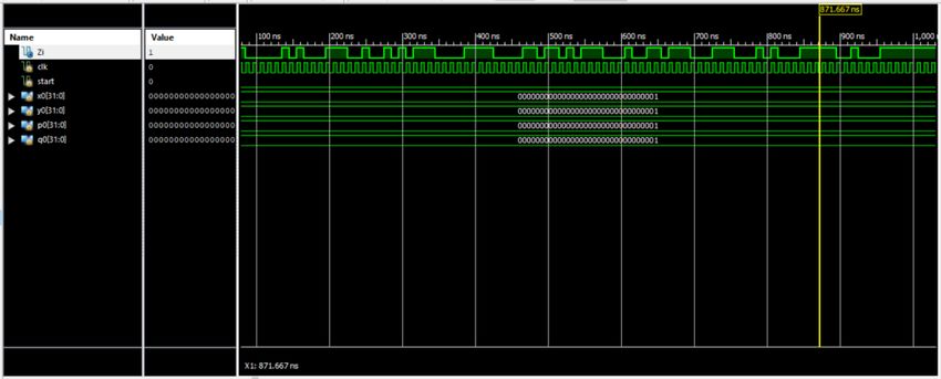
Vol 13, Issue 05, May / 2022
                                                                                              ISSN NO: 0377-9254

          efficient Montgomery multiplication algorithm. Here a modification in the form of using hybrid full
          adders in the Carry Save adder is proposed. The hybrid full adder is designed using a conventional
          Complementary Metal Oxide Semiconductor and transmission gate logic. There is about 54% and 55%
          reduction of area (no. of components) in Radix 2 MMM and Semi-Carry-Save (SCS) based MMM with
          hybrid full adders. There is significant reduction in the power dissipation of 52% for Radix 2 MMM
          and 46% of SCS based MMM when hybrid adders are used instead of C-CMOS Full-Adders. The delay
          is also reduced by 47% in SCS based MMM as compared to that of Radix 2 MMM. The software used
          are Xilinx ISE 14.2 and Mentor Graphics Pyxis Schematic in 180-nm technology. S.-R. Kuang, J.-P.
          Wang, K.-C. Chang, and H.-W. Hsu, “Energy-efficient high-throughput montgomery modular
          multipliers for RSA cryptosystems,”For future internet services and data communication systems,
          it is identified that security matters become questionable and problematical. Cryptographic
          algorithms are a convenient tool for achieving security in those systems. So, realization of
          cryptographic systems in hardware is more advantageous. Of the two-broad category of
          cryptographic systems as public key cryptosystems and secret key cryptosystems, public key
          cryptosystems are widely used. In many public key cryptosystems, the key operation is modular
          multiplication with large input operands. The trial division in modular multiplication is time
          consuming. So, well-known algorithm called Montgomery modular multiplication algorithm is
          introduced by avoiding the trial division. Shifting modular additions are used instead of
          complicated division operations. Different modifications to conventional Montgomery modular
          multiplications are proposed to reduce the delay associated with the long carry propagation in the
          computation of intermediate result. This paper explores a comparison between two modification
          algorithms to conventional Montgomery MM algorithms.S. S. Erdem, T. Yanik, and A. Celebi, “A
          general digit-serial architecture for montgomery modular multiplication,” Multiplication is a key
          operation to perform the processing speed of digital processor. Montgomery multiplication is a strategy
          for performing quick modular multiplication. This paper presents an outline on execution of
          Montgomery measured duplication estimation utilizing VLSI design. The Montgomery figuring is a
          fast particular increase procedure as regularly as conceivable used in cryptographic applications, in
          which the capability of cryptosystem depends upon the speed of secluded duplication. This audit gives
          the assessment between different adjustments done in Montgomery particular augmentation. K. Panda
          and K. C. Ray, “Modified dual-CLCG method and its VLSI architecture for pseudorandom bit
          generation,” The dual coupled-LCG (dual-CLCG) is a secure pseudorandom bit generator (PRBG)
          method amongst various LFSR, LCG and chaotic based PRBG methods for generating a pseudorandom
          bit sequence. The hardware implementation of this method has a bottleneck due to the involvement of
          inequality equations. Initially, a direct architectural mapping of the dual-CLCG method is performed.
          Since two inequality equations are involved for coupling, it generates pseudorandom bit at unequal
          interval of time that leads to large variation in output latency. Besides, it consumes a large area and fails
          to achieve the maximal period. Hence, to overcome the aforesaid drawbacks, a new efficient PRBG
          method, i.e., "coupled variable input LCG (CVLCG)" and its architecture are proposed. The novelty of
          the proposed method is the coupling of two newly formed variable input LCGs that generates
          pseudorandom bit at every uniform clock rate, In order to increase the performance of the adders, there
          are two methods which are being considered for this project: Boolean Simplification and Transistor
          Sizing. Boolean Simplification is a method of simplification of Boolean equations to the simplest
          equation form which use less inputs in the equation. Transistor sizing is one of the existing performance
          optimization techniques which IC designers have usually relied on in order to improve the switching
          speed of CMOS VLSI circuits. Transistor sizing is a very effective technique in order to optimize a
          circuit in terms of power as well as speed. K. S. Pandey, D. K. B. N. Goel, and H. Shrimali, “An ultra-
          fast parallel prefix adder,” in Proc. IEEE 26th Symp. Comput. Arithmetic (ARITH), To overcome this
          disadvantage, we need a new area efficient and high-speed adder architecture to be proposed using pre

www.jespublication.com                                                                                       Page No:504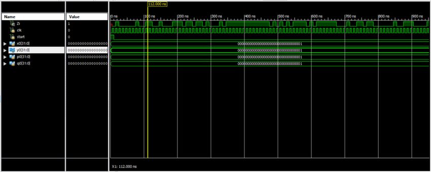
Vol 13, Issue 05, May / 2022
                                                                                            ISSN NO: 0377-9254

          compute bitwise addition followed by carry prefix computation logic to perform three operand binary
          adder which reduces delay and area efficiently. This method is the proposed method and implemented
          on the FPGA device. A newly designed three operand binary adder is shown and is implemented in
          MDCLCG. The results of 16 bit and 32-bit three operand adder will be shown and this proposed method
          is applied on Modified Dual CLCG. The Carry-Save-Adder architecture used in 32-bit MDCLCG is
          replaced by the proposed architecture. The design is prototyped on a commercially available FPGA
          platform to validate the design on silicon chip.

          3. RESULTS
              The RTL schematic is abbreviated as the register transfer level it denotes the blue print of the
          architecture and is used to verify the designed architecture to the ideal architecture that we are in need
          of development .The hdl language is used to convert the description or summery of the architecture to
          the working summery by use of the coding language i.e verilog ,vhdl. The RTL schematic even specifies
          the internal connection blocks for better analyzing .The figure represented below shows the RTL
          schematic diagram of the designed architecture.

                                        Fig.1 RTL Schematic of existed MDCLCG.

                                       Fig. 2 RTL Schematic of Proposed MDCLCG

          TECHNOLOGY SCHEMATIC: The technology schematic makes the representation of the
          architecture in the LUT format, where the LUT is consider as the parameter of area that is used in VLSI
          to estimate the architecture design. The LUT is consider as an square unit the memory allocation of the
          code is represented in there LUT s in FPGA.
          SIMULATION:
          The simulation is the process which is termed as the final verification in respect to its working where

www.jespublication.com                                                                                     Page No:505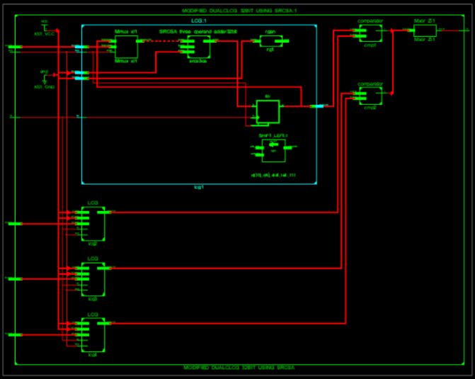
Vol 13, Issue 05, May / 2022
                                                                                          ISSN NO: 0377-9254

          as the schematic is the verification of the connections and blocks. The simulation window is launched
          as shifting from implantation to the simulation on the home screen of the tool ,and the simulation
          window confines the output in the form of the wave forms. Here it has the flexibility of providing the
          different radix number systems.

                                        Fig. 3 Simulated Waveforms of existed MDCLCG

                                        Fig. 4 Simulated Waveforms of proposed MDCLCG
          The simulation is the process which is termed as the final verification in respect to its working where
          as the schematic is the verification of the connections and blocks. The simulation window is launched
          as shifting from implantation to the simulation on the home screen of the tool, and the simulation
          window confines the output in the form of the wave forms. Here it has the flexibility of providing the
          different radix number systems.
          PARAMETERS:
                   Consider in VLSI the parameters treated are area, delay and power, based on these parameters
          one can judge the one architecture to other. here the consideration of delay is considered the parameter
          is obtained by using the tool XILINX 14.7 and the HDL language is verilog language.

www.jespublication.com                                                                                   Page No:506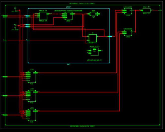
Vol 13, Issue 05, May / 2022
                                                                                          ISSN NO: 0377-9254

          5. CONCLUSION
          Modified Dual-CLCG method involves dual coupling of four LCGs that makes it more secure than
          LCG based PRBGs. However, it is reported that this method has the drawback of generating
          pseudorandom bit at large area and more delay. proposed architecture of the new modified dual- CLCG
          method using square root carry select adder is significantly reduced the area of the design.

          REFERENCES
          [1] M. M. Islam, M. S. Hossain, M. K. Hasan, M. Shahjalal, and Y. M. Jang, “FPGA implementation
          of high-speed area-efficient processor for elliptic curve point multiplication over prime field,” IEEE
          Access, vol. 7, pp. 178811–178826, 2019.
           [2] Z. Liu, J. GroBschadl, Z. Hu, K. Jarvinen, H. Wang, and I. Verbauwhede, “Elliptic curve
          cryptography with efficiently computable endomorphisms and its hardware implementations for the
          Internet of Things,” IEEE Trans. Comput., vol. 66, no. 5, pp. 773–785, May 2017.
          [3] Z. Liu, D. Liu, and X. Zou, “An efficient and flexible hardware implementation of the dual-field
          elliptic curve cryptographic processor,” IEEE Trans. Ind. Electron., vol. 64, no. 3, pp. 2353–2362, Mar.
          2017.
          [4]B. Parhami, Computer Arithmetic: Algorithms and Hardware Design. New York, NY, USA: Oxford
          Univ. Press, 2000.
          [5] P. L. Montgomery, “Modular multiplication without trial division,” Math. Comput., vol. 44, no.
          170, pp. 519–521, Apr. 1985.
          [6] S.-R. Kuang, K.-Y. Wu, and R.-Y. Lu, “Low-cost high-performance VLSI architecture for
          montgomery modular multiplication,” IEEE Trans. Very Large Scale Integr. (VLSI) Syst., vol. 24, no.
          2, pp. 434–443, Feb. 2016.
          [7] S.-R. Kuang, J.-P. Wang, K.-C. Chang, and H.-W. Hsu, “Energy-efficient high-throughput
          montgomery modular multipliers for RSA cryptosystems,” IEEE Trans. Very Large Scale Integr.
          (VLSI) Syst., vol. 21, no. 11, pp. 1999–2009, Nov. 2013.
          [8] S. S. Erdem, T. Yanik, and A. Celebi, “A general digit-serial architecture for montgomery modular
          multiplication,” IEEE Trans. Very Large Scale Integr. (VLSI) Syst., vol. 25, no. 5, pp. 1658–1668, May
          2017.
          [9] R. S. Katti and S. K. Srinivasan, “Efficient hardware implementation of a new pseudo-random bit

www.jespublication.com                                                                                   Page No:507
Vol 13, Issue 05, May / 2022
ISSN NO: 0377-9254
sequence generator,” in Proc. IEEE Int. Symp. Circuits Syst., Taipei, Taiwan, May 2009, pp. 1393–
1396.
[10] A. K. Panda and K. C. Ray, “Modified dual-CLCG method and its VLSI architecture for
pseudorandom bit generation,” IEEE Trans. Circuits Syst. I, Reg. Papers, vol. 66, no. 3, pp. 989–1002,
Mar. 2019.
[11] A. Kumar Panda and K. Chandra Ray, “A coupled variable input LCG method and its VLSI
architecture for pseudorandom bit generation,” IEEE Trans. Instrum. Meas., vol. 69, no. 4, pp. 1011–
1019, Apr. 2020.
[12] N. Weste and K. Eshraghian, Principles of CMOS VLSI Design—A Systems Perspective. Reading,
MA, USA: Addison-Wesley, 1985.
[13] T. Kim, W. Jao, and S. Tjiang, “Circuit optimization using carry-saveadder cells,” IEEE Trans.
Comput.-Aided Design Integr. Circuits Syst., vol. 17, no. 10, pp. 974–984, Oct. 1998. [14] A. Rezai
and P. Keshavarzi, “High-throughput modular multiplication and exponentiation algorithms using
multibit-scan–multibit-shift technique,” IEEE Trans. Very Large Scale Integr. (VLSI) Syst., vol. 23,
no. 9, pp. 1710–1719, Sep. 2015.
[15] A. K. Panda and K. C. Ray, “Design and FPGA prototype of 1024- bit Blum-Blum-Shub PRBG
architecture,” in Proc. IEEE Int. Conf. Inf. Commun. Signal Process. (ICICSP), Singapore, Sep. 2018,
pp. 38–43.
[16] T. Han and D. A. Carlson, “Fast area-efficient VLSI adders,” in Proc. IEEE 8th Symp. Comput.
Arithmetic (ARITH), May 1987, pp. 49–56.
www.jespublication.com Page No:508You can also read