Four-Dimensional Scanning Transmission Electron Microscopy (4D-STEM): From Scanning Nanodiffraction to Ptychography and Beyond
←
→
Page content transcription
If your browser does not render page correctly, please read the page content below
Microscopy and Microanalysis (2019), 25, 563–582
           doi:10.1017/S1431927619000497

           Review Article

           Four-Dimensional Scanning Transmission Electron Microscopy
           (4D-STEM): From Scanning Nanodiffraction to Ptychography
           and Beyond
           Colin Ophus*
           National Center for Electron Microscopy, Molecular Foundry, Lawrence Berkeley National Laboratory, 1 Cyclotron Road, Berkeley, CA, USA

           Abstract
           Scanning transmission electron microscopy (STEM) is widely used for imaging, diffraction, and spectroscopy of materials down to atomic
           resolution. Recent advances in detector technology and computational methods have enabled many experiments that record a full image of
           the STEM probe for many probe positions, either in diffraction space or real space. In this paper, we review the use of these four-dimen-
           sional STEM experiments for virtual diffraction imaging, phase, orientation and strain mapping, measurements of medium-range order,
           thickness and tilt of samples, and phase contrast imaging methods, including differential phase contrast, ptychography, and others.
           Key words: transmission electron microscopy (TEM), four dimensional-scanning transmission electron microscopy (4D-STEM), scanning
           electron nanodiffraction (SEND), nanobeam electron diffraction (NBED)
           (Received 16 January 2019; revised 9 March 2019; accepted 19 March 2019)

           Introduction                                                                               plane in the far field. Note that in Figure 1, the diffraction images
                                                                                                      are displaced from each other in order not to overlap, but in real-
           Transmission electron microscopy (TEM) is one of the most power-
                                                                                                      ity all images are measured at the same detector position.
           ful characterization tools available to researchers studying nanoscale
                                                                                                          Each image in Figure 1 is an average of 49 adjacent probe
           structures and phenomena. The unmatched spatial resolution of
                                                                                                      images (in a 7 × 7 grid), where each image is approximately four
           TEM, with the high degree of flexibility afforded by electromagnetic
                                                                                                      megapixels. This gives a total dataset size of 420 GB, recorded in
           lenses and multipoles, and the large number of potential measure-
                                                                                                      164 s. Large-scale four-dimensional (4D)-STEM experiments
           ment channels have led to the development of many different oper-
                                                                                                      such as this one have become possible because of two develop-
           ating modes for TEM. Scanning transmission electron microscopy
                                                                                                      ments: high speed and efficient direct electron detectors, and
           (STEM), in particular, can perform a large number of different mea-
                                                                                                      the widespread availability of computational power.
           surements, many of them simultaneously. This is because in STEM
                                                                                                          The name “4D-STEM” refers to recording 2D images of a con-
           the electron probe is focused onto the sample surface and thus has a
                                                                                                      verged electron probe, over a 2D grid of probe positions. The
           very small spatial extent, down to sub-atomic dimensions. After the
                                                                                                      resulting datasets are 4D, hence the term 4D-STEM, by which we
           STEM probe scatters from the sample, signals that can be measured
                                                                                                      mean all forms of scattering measurements where 2D images of a
           include the forward diffracted electrons for various subsets of
                                                                                                      STEM probe are recorded, either in real or diffraction space, for a
           momenta, back-scattered electrons, X-rays, and secondary electrons
                                                                                                      2D grid of probe positions. This paper will review many different
           generated inside the sample, and the energy loss spectroscopic signal.
                                                                                                      forms of 4D-STEM measurements, their history, and some recent
           In this paper, we focus primarily on momentum-resolved measure-
                                                                                                      developments. We will also discuss naming conventions, electron
           ments of the forward scattered electrons, especially those scattered
                                                                                                      detector development, and simulation of 4D-STEM datasets.
           elastically. Information on STEM development can be found in
           Pennycook & Nellist (2011) and other TEM textbooks.
               Figure 1 shows a momentum-resolved STEM experimental                                   Basics of 4D-STEM
           dataset measured from a dichalcogenide two-dimensional (2D)                                Naming Conventions
           material. The STEM probe is formed by TEM condenser optics
           and possibly aberration-corrected. Next, it is focused on the sam-                         The name “4D-STEM” is widely used in the literature, for example
           ple surface, where it propagates through and scatters. After exiting                       in Ophus et al. (2014), Yang et al. (2015a), Ryll et al. (2016), Wang
           the sample, the probe is magnified and measured on the detector                            et al. (2018), Fatermans et al. (2018), Xu & LeBeau (2018), Hachtel
                                                                                                      et al. (2018), and Mahr et al. (2019), though this name is far from
                                                                                                      universal. Note that it has also been used in the past to refer to
             *Author for correspondence: Colin Ophus, E-mail: cophus@gmail.com
             Cite this article: Ophus C (2019) Four-Dimensional Scanning Transmission Electron
                                                                                                      combination STEM electron energy loss spectroscopy (EELS)
           Microscopy (4D-STEM): From Scanning Nanodiffraction to Ptychography and Beyond.            and tomography, which also produces a 4D dataset. This tech-
           Microsc Microanal 25, 563–582. doi:10.1017/S1431927619000497                               nique however is typically referred to as “4D-STEM-EELS,” for
           © Microscopy Society of America 2019. This is an Open Access article, distributed under the terms of the Creative Commons Attribution licence (http://creativecommons.org/licenses/
           by/4.0/), which permits unrestricted re-use, distribution, and reproduction in any medium, provided the original work is properly cited.

Downloaded from https://www.cambridge.org/core. IP address: 46.4.80.155, on 21 Jan 2022 at 12:30:25, subject to the Cambridge Core terms of use, available at https://www.cambridge.org/core/terms.
https://doi.org/10.1017/S1431927619000497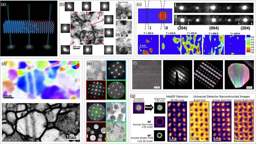
564                                                                                                                                                              Colin Ophus

                                                                                                     method is called “automated crystal orientation mapping”
                                                                                                     (ACOM), for example in Schwarzer & Sukkau (1998), Seyring
                                                                                                     et al. (2011), Kobler et al. (2013), Izadi et al. (2017), and others.
                                                                                                         Conventional STEM detectors record one value per pixel and
                                                                                                     usually have an annular (ring or circular) geometry. Common
                                                                                                     imaging modes include bright field (BF) where the detector is
                                                                                                     aligned with all or part of the unscattered probe, annular bright
                                                                                                     field (ABF) where a circle is removed from the center of the detec-
                                                                                                     tor, and annular dark field (ADF) which selects an angular range
                                                                                                     of electrons scattered outside of the initial STEM probe. A very
                                                                                                     common STEM imaging mode is high-angle ADF (HAADF),
                                                                                                     which records only the incoherent signal of the thermal diffuse
                                                                                                     scattering (TDS) electrons, due to its easy interpretation
                                                                                                     (Pennycook & Nellist, 2011).
                                                                                                         In this manuscript, we have chosen to use the general term of
                                                                                                     4D-STEM in order to include imaging methodologies where the
                                                                                                     probe is recorded in real space, for example in (Nellist et al.,
                                                                                                     2006; Zaluzec, 2007; Etheridge et al., 2011).
          Fig. 1. Experimental 4D-STEM measurement of a dichalcogenide 2D material. Atomic
          map is inferred from the data, each diffraction pattern represents an average of 7 × 7
          experimental images, green STEM probes are labeled for regions of the sample with          Detector Development
          one layer, vacuum, and two layers.
                                                                                                     The rise of popularity for 4D-STEM measurements is directly
                                                                                                     linked to the availability of high performance electron detector tech-
          example in Jarausch et al. (2009), Florea et al. (2012), Goris et al.                      nology. Conventional STEM detectors for BF, ABF, ADF, and
          (2014), and Midgley & Thomas (2014). Related terms for images                              HAADF record only a single value per STEM probe position, and
          of STEM diffraction patterns in common use from the literature                             segmented detectors with 4–16 channels are used for differential
          include “convergent beam electron diffraction” (CBED), “micro-                             measurements (Haider et al., 1994). Currently, the most common
          diffraction,” “nanodiffraction,” “diffraction imaging,” and “diffrac-                      detector configuration recording full images in TEM is a charge
          togram,” all of which refer to diffraction images of a converged                           coupled device (CCD) with digital readout, coupled with a scintil-
          electron probe. The term “ronchigram” is named for the                                     lator, such as in Fan & Ellisman (1993) and De Ruijter (1995).
          “Ronchi test” for measuring aberrations of telescope mirrors and                           These detectors have good electron sensitivity, but typically have
          other optical elements, developed by Ronchi (1964). STEM                                   readout speeds limited to video rate (≤60 frames/s) and limited
          probe diffraction measurements of aberrations using periodic                               dynamic range. This makes CCDs ill-suited to 4D-STEM diffraction
          objects were introduced by Cowley & Spence (1979) and were                                 imaging, which requires readout speeds comparable with the STEM
          referred to as ronchigrams by Cowley (1986). Today the term usu-                           probe scanning rate (μs to ms timescales) and the ability to measure
          ally refers to a diffraction image that is nearly in focus, typically                      high-intensity signals such as the BF disk and low-intensity signals
          recorded from an amorphous material.                                                       such as the high-angle scattered electrons simultaneously.
              Some of the earliest experiments that could be classified as                               There are two primary routes to building detectors more
          4D-STEM in the sense of this paper were those performed by                                 suitable for 4D-STEM applications. The first detector type is
          Zaluzec (2002) to measure the Lorentz deflection. Zaluzec referred                         monolithic active pixel sensors (APS), which are complementary
          to this method as “position resolved diffraction” (PRD) in accor-                          metal–oxide–semiconductor (CMOS) chips with a sensitive doped
          dance with earlier work where 2D diffraction patterns were                                 epitaxial layer. When high energy electrons pass through this
          recorded over a line scan. The term PRD is more often found in                             layer, many low energy electrons are generated, which diffuse
          the X-ray diffraction literature, but can still be found in the TEM                        toward sensor diodes where they are collected and read out
          literature, for example in Chen et al. (2016). The similar term “spa-                      using CMOS electronics, as described in Mendis et al. (1997),
          tially resolved diffractometry” was also used by Kimoto & Ishizuka                         Dierickx et al. (1997), and Milazzo et al. (2005). APS direct
          (2011), which they used to refer to virtual imaging in 4D-STEM.                            electron detectors have seen widespread deployment after being
          The term “momentum-resolved STEM” is also used by some                                     commercialized by several companies, for example in Ryll et al.
          authors, for example Müller-Caspary et al. (2018a).                                        (2016). See McMullan et al. (2014) for a performance compari-
              Perhaps the most common alternative name for a 4D-STEM                                 son. APS detectors have very high sensitivities and fast readout
          measurement in diffraction space is “scanning electron nanodiffrac-                        speed, but relatively poor dynamic range. For high efficiency
          tion”, used by Tao et al. (2009), Liu et al. (2013), Gallagher-Jones                       imaging, single “electron counting” is typically applied to images
          et al. (2019), and many others. A similar descriptor used in many                          recorded with APS detectors (Li et al., 2013). This requires many
          studies is “nanobeam electron diffraction” (NBED), used for example                        pixels and relatively low electron doses in order to reduce the
          by Clément et al. (2004), Hirata et al. (2011), and Ozdol et al. (2015).                   electron density recorded in each image to roughly less than 0.1
          The term “pixelated STEM” can also be found in the literature, for                         electrons per pixel per frame, since high densities prevent locali-
          example in MacArthur et al. (2013). In addition to referring to pix-                       zation of individual electron strikes. If these conditions are met,
          elated STEM, Hachtel et al. (2018) also introduced the term “univer-                       electron counting can maximize the efficiency of 4D-STEM
          sal detector” to refer to virtual imaging in 4D-STEM.                                      experiments, see Gallagher-Jones et al. (2019) for example. Note
              One 4D-STEM application discussed extensively below is crys-                           that because the design of APS detector pixels is relatively simple,
          tal orientation mapping. When using computer image processing                              these detectors typically contain a large number of pixels which
          methods to classify the crystal orientations automatically, this                           decreases the electron density in each pixel.

Downloaded from https://www.cambridge.org/core. IP address: 46.4.80.155, on 21 Jan 2022 at 12:30:25, subject to the Cambridge Core terms of use, available at https://www.cambridge.org/core/terms.
https://doi.org/10.1017/S1431927619000497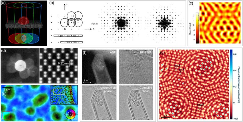
Microscopy and Microanalysis                                                                                                                                                 565

               The second kind of detector used in modern 4D-STEM experi-                             each probe location. This removes one of the weaknesses of con-
           ments is a hybrid pixel array detector (PAD). In this type of detec-                       ventional STEM imaging; namely that a small number of bright
           tor, an array of photodiodes is bump bonded to an                                          and dark field detectors must be physically positioned at some
           application-specific integrated circuit, described in Ansari et al.                        angle from the optical axis, and cannot be changed relative to
           (1989), Ercan et al. (2006), and Caswell et al. 2009). PADs have                           each other during the measurements. After a conventional
           been optimized for 4D-STEM experiments by using high-gain inte-                            STEM measurement, electrons within the scattering range are
           gration and counting circuitry in each pixel, giving single electron                       grouped together and can no longer be further separated by scat-
           sensitivity, high dynamic range, and fast readout speeds (Tate                             tering angle. Note that nanodiffraction has been used for materi-
           et al., 2016). This detector has also been commercialized and used                         als science investigations for a long time (Cowley, 1996). However,
           for many 4D-STEM experiments, for example in Jiang et al. (2018).                          here we will review only 4D-STEM virtual imaging experiments,
                                                                                                      i.e., the sort of position-resolved nanodiffraction studies suggested
                                                                                                      by Zaluzec (2003) or shown experimentally such as Fundenberger
           Computational Methods                                                                      et al. (2003), Lupini et al. (2015), and (Fatermans et al. (2018),
           Almost every study described in this review uses computational                             and those which use such images to perform structural classifica-
           imaging in some capacity. The digital recording of microscopy                              tion as in the schematic plotted in Figure 2a.
           images and diffraction patterns quickly replaced the previously                                 Figure 2 shows a 4D-STEM experiment imaging Y-doped
           used film technology in no small part because it made it easy to                           ZrO2 performed by Watanabe & Williams (2007). Two methods
           use computers to analyze the resulting data. This review will not                          to interpret such a measurement are both shown: either selecting
           explicitly cover data recording, processing, and analysis methods.                         diffraction patterns from different regions of constant contrast
           Instead we will provide a non-exhaustive list of code repositories                         over the probe positions in real space, or generating a virtual
           that are currently being developed for 4D-STEM data analysis.                              detector from subsets of pixels in the reciprocal space diffraction
           These include: HyperSpy, pyXem, LiberTEM, Pycroscopy and                                   pattern coordinate system. A similar experiment was performed
           py4DSTEM. Because so many of the 4D-STEM methods and                                       by Schaffer et al. (2008), where first virtual dark field images
           technologies shown in this paper are being actively developed,                             were formed from regions of interest in the real space image along
           we expect the software landscape to change considerably in the                             an interface. Then, virtual detectors were applied to resulting
           near future. We also want to encourage the vendors of commer-                              spots in the diffraction patterns to form improved dark field
           cial electron microscopes and detectors to allow full program-                             images and combined into a single RGB color map. Tao et al.
           matic control of instrumentation in order to implement and                                 (2009) used a similar approach, shown in Figure 2c, to map out the
           optimize 4D-STEM experiments, and to use open source file for-                             positions of a nanoscale precipitate phase in La0.55Ca0.45MnO3 as
           mats for data and metadata.                                                                a function of sample temperature, using superlattice reflections.
                                                                                                      Zhang et al. (2017) have also performed phase mapping of beam-
                                                                                                      sensitive battery cathode materials using diffraction mapping.
           Precession Electron Diffraction                                                                 Advancing detector technology and increased stability of TEM
           Diffraction patterns from thicker samples can contain significant                          instruments and sample stages has led to continual improvement
           multiple scattering (i.e., dynamical diffraction). This leads to dif-                      in 4D-STEM diffraction mapping. Figure 2d shows the complex
           fraction patterns where the average intensities of the Bragg disks                         microstructure of a nanocrystalline copper sample mapped by
           are very uniform (i.e., structure factor details are lost), and a sig-                     Caswell et al. (2009) using both diffraction spot orientation map-
           nificant amount of fine structure generated inside each disk. Both                         ping and correlation of adjacent diffraction patterns. Diffraction
           of these effects can make indexing and quantitative intensity mea-                         mapping at atomic resolution was demonstrated by Kimoto &
           surements of Bragg spots more difficult. One method to minimize                            Ishizuka (2011), who recorded diffraction patterns from individ-
           multiple scattering is to collect an average diffraction pattern from                      ual atomic columns in SrTiO3. Diffraction mapping capability
           many incident beam tilt directions, which is called “precession                            with full control of the beam tilts before and after the sample
           electron diffraction” (PED), or scanning-PED. Introduced by                                was demonstrated by Koch et al. (2012). Jones & Nellist (2013)
           Vincent & Midgley (1994), PED uses deflection coils above and                              discussed the use of virtual detectors for imaging in 4D-STEM.
           below the sample in order to tilt the angle of the beam incident                                Figure 2e shows both virtual detectors in real space and dif-
           on the sample, and then precess the beam through a range of                                fraction space of a 4D-STEM measurement of an Fe–Al–Ni–Cr
           azimuthal tilts. This “hollow cone” illumination integrates over                           alloy measured by Gammer et al. (2015). Zeng et al. (2015)
           excitation errors of different beams, which somewhat reduces                               used nanodiffraction mapping to characterize residual MoS2
           dynamical scattering effects, and has found widespread applica-                            products from nanosheets, after an electrochemical reaction in a
           tion in electron crystallography (Midgley & Eggeman, 2015). As                             liquid cell. Figure 2f shows virtual detectors applied to measure
           will be shown below, PED has been applied to many different                                presence of three ordering variants of a battery cathode material
           4D-STEM measurements. When combined with NBED measure-                                     by Shukla et al. (2016). This example shows how 4D-STEM can
           ments, this technique is sometimes referred to as “nanobeam pre-                           in many cases obtain the same information as atomic-resolution
           cession electron diffraction”, as in Rouviere et al. (2013).                               HRTEM or conventional STEM images, but over a far larger field
                                                                                                      of view (FOV), a method used again in Shukla et al. (2018). An
                                                                                                      example of virtual annular detectors is shown in Figure 2g,
           Structure and Property Measurements                                                        from an experiment by (Hachtel et al., 2018) imaging a
                                                                                                      DyScO3 sample at atomic resolution. Wang et al. (2018) have pro-
           Virtual Imaging and Structure Classification
                                                                                                      posed methods for correcting sample drift both in STEM-EELS
           One of the most obvious uses of 4D-STEM diffraction imaging is                             and 4D-STEM experiments. Li et al. (2019) have used machine
           the ability to use arbitrary “virtual” detectors by adding (or sub-                        learning methods to extract atomic-resolution defect information
           tracting) some subset of the pixels in the diffraction patterns at                         from 4D-STEM datasets.

Downloaded from https://www.cambridge.org/core. IP address: 46.4.80.155, on 21 Jan 2022 at 12:30:25, subject to the Cambridge Core terms of use, available at https://www.cambridge.org/core/terms.
https://doi.org/10.1017/S1431927619000497
566                                                                                                                                                              Colin Ophus

          Fig. 2. Virtual imaging and classification in 4D-STEM. a: Schematic showing how properties such as local ordering can be directly determined from diffraction
          patterns. b: 4D-STEM experiment of Y-doped ZrO2 from Watanabe & Williams (2007), showing both diffraction patterns from different probe positions and images
          generated from virtual detectors in diffraction space. c: Nanoscale precipitate phase in La0.55Ca0.45MnO3 mapped from superlattice reflections, adapted from Tao
          et al. (2009). d: Top panel shows diffraction spot orientation and bottom panel shows correlation between adjacent diffraction patterns for a nanocrystalline Cu
          sample, adapted from Caswell et al. (2009). e: Top panel shows mean diffraction patterns from ROIs in real space, bottom panel shows virtual images generated
          from ROIs in diffraction space, from Gammer et al. (2015). f: Images from left-to-right are an HRTEM image of cathode material at atomic resolution showing three
          stacking variants, mean diffraction pattern, virtual detectors, and output RGB image showing outputs of virtual detectors, from Shukla et al. (2016). g: Virtual
          annular detectors at atomic resolution for a DyScO3 sample, from Hachtel et al. 2018).

              More exotic property measurements are also possible with                               to TEM experiments in order to increase resolution of orientation
          4D-STEM experiments. Wehmeyer et al. (2018) used virtual aper-                             maps. In TEM diffraction imaging, orientation of a crystalline
          tures to measure thermal diffuse scattering between Bragg disks as                         sample can be determined by either fitting Kikuchi diffraction
          a measurement of local temperature. Tao et al. (2016) used                                 patterns (Kikuchi, 1928) plotted in Figure 3a, or by direct index-
          4D-STEM to study electronic liquid–crystal phase transitions                               ing of the scattered Bragg spots or disks (Schwarzer, 1990) as
          and their microscopic origin, and Hou et al. (2018) used it to                             shown in Figure 3b. Bragg spot indexing in 4D-STEM is essen-
          measure the degree of crystallinity in metal–organic-frameworks                            tially a form of selected area diffraction, where the “area” selected
          (MOFs). We expect that as pixelated detectors fall in price and                            is the region illuminated by the STEM probe. Both methods are
          larger amounts of computational power are available at the micro-                          qualitatively similar, but each has strengths and weaknesses.
          scope, virtual imaging will become a very common operating                                 Generally, spot indexing is better for thinner specimens, while
          mode for 4D-STEM. Commercial software to automate crystallo-                               Kikuchi diffraction performs better for thicker samples (as forma-
          graphic phase mapping is already available, see for example Rauch                          tion of Kikuchi bands relies on a sufficient diffuse scattering being
          et al. (2010), combined with PED, which was described in a pre-                            present). Additionally, the orientation precision tends to be higher
          vious section of this paper. It has been used in various materials                         for Kikuchi diffraction due to the sharpness of the features
          science studies, including, for example Brunetti et al. (2011), who                        measured, but it can fail in regions of high local deformation
          used it to understand Li diffusion in battery materials.                                   when the line signal becomes too delocalized. See Zaefferer
                                                                                                     (2000), Zaefferer (2011), and Morawiec et al. (2014) for further
                                                                                                     information comparing these methods.
          Crystalline and Semicrystalline Orientation Mapping
                                                                                                         Early implementations of orientation mapping in TEM did not
          An important subset of structure classification for materials                              have the computer memory or disk space to record every diffrac-
          science is orientation mapping, and so we discuss it separately                            tion pattern for later analysis. Instead, patterns were typically
          here. Electron backscatter diffraction using scanning electron                             acquired and indexed online. An early implementation of orien-
          microscopy (SEM) is the most commonly employed method to                                   tation mapping using Kikuchi patterns was developed by
          measure 2D maps of orientation distributions in crystalline mate-                          Fundenberger et al. (2003). Figure 3c shows one of these measure-
          rials, reviewed in Wright et al. (2011). Schwarzer & Sukkau (1998)                         ments, how it is high pass filtered and then fitted with an indexed
          also reviewed ACOM methods for measuring maps of crystalline                               line pattern, and finally an output orientation map for a deformed
          grain orientations in SEM and suggested their future applicability                         aluminum sample. As shown in Figure 2b, Watanabe & Williams

Downloaded from https://www.cambridge.org/core. IP address: 46.4.80.155, on 21 Jan 2022 at 12:30:25, subject to the Cambridge Core terms of use, available at https://www.cambridge.org/core/terms.
https://doi.org/10.1017/S1431927619000497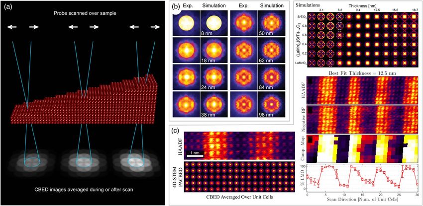
Microscopy and Microanalysis                                                                                                                                                 567

           Fig. 3. Orientation mapping in 4D-STEM, using (a) Kikuchi patterns, or (b) Bragg disk diffraction. c: Kikuchi patterns indexing and orientation map of aluminum,
           adapted from Fundenberger et al. (2003). d: Orientation of Bragg disk pattern estimated with template matching, and resulting correlation scores for all orienta-
           tions, by Rauch & Dupuy (2005). e: Simultaneous phase and orientation determination for LiFePO4, from Brunetti et al. (2011). f: In-situ orientation mapping of
           nanocrystalline Au during a mechanical test, from Kobler et al. (2013). g: Orientation map of a biological peptide crystal, from Gallagher-Jones et al. (2019).

           (2007) performed a very early 4D-STEM experiment where a                                   pathway model for this material, thus highlighting the usefulness
           Kikuchi diffraction orientation map could be constructed from                              of “plug and play” methods for TEM phase and orientation map-
           a 4D-STEM scan. The Kikuchi method has been applied in                                     ping. Kobler et al. (2013) extended ACOM experiments to in-situ
           many materials science studies, for example to a TiAl alloy by                             mechanical testing measurements of nanocrystalline Au, with an
           Dey et al. (2006), to cold-rolling of Ti by Bozzolo et al. (2007),                         example shown in Figure 3f. In this example, the misorientation
           to ferroelectric domains by MacLaren et al. (2010), and others.                            angle of many grains was measured as a function of the loading
           Note that Kikuchi pattern orientation mapping can also be per-                             force. These and many other statistics can be obtained simultane-
           formed in an SEM; this method has been demonstrated by                                     ously using time-resolved ACOM. Other examples of in-situ stud-
           Trimby (2012) and Brodusch et al. (2013).                                                  ies include: Idrissi et al. (2014), Garner et al. (2014), Bufford et al.
               An example of orientation mapping using Bragg spots is                                 2015), Izadi et al. 2017), Guo & Thompson (2018), and others. An
           shown in Figure 3d from Rauch & Dupuy (2005). They intro-                                  extreme example of orientation mapping was recently published
           duced a fast “template matching” procedure, where the diffraction                          by Bruma et al. (2016), who analyzed beam-induced rotation of
           patterns are pre-computed for each orientation of a given mate-                            102-atom Au clusters.
           rial, and then, as shown in Figure 3d, a correlation score is com-                             Orientation maps can also be determined for semicrystalline
           puted for each experimental pattern. This method can be fully                              materials, such as small molecule assemblies or polymers. One
           automated, and can also generate an estimate of the measurement                            such example was shown by Panova et al. (2016), who mapped
           confidence using the maximum correlation score (Rauch et al.,                              the degree of crystallinity and orientation of a polymer sample.
           2010). Combined with PED, phase and orientation mapping has                                Bustillo et al. (2017) extended this method to include multiple soft
           been commercialized and widely deployed (Darbal et al., 2012). A                           matter samples, including organic semiconductors. Mohammadi
           review of these methods for automated orientation mapping is                               et al. (2017) have also performed orientation mapping of semi-
           given in Rauch & Véron (2014). The combination of scanning dif-                            conducting polymers using 4D-STEM. They employed a statistical
           fraction measurements, PED, and sample tilt to create 3D orien-                            approach to measure the angular deviation of the π − π stacking
           tation tomographic reconstructions was shown by Eggeman et al.                             direction over a very large FOV. Orientation mapping has even
           (2015). Other extensions to orientation mapping include applying                           been applied to peptide crystals, in the study by Gallagher-Jones
           principal component analysis and machine learning techniques to                            et al. (2019) which analyzed small magnitude ripples, as shown
           orientation measurements in 4D-STEM datasets, for example in                               in Figure 3g. The ability to use very low electron currents, small
           studies by Sunde et al. (2018) and Ånes et al. (2018).                                     convergence angle (large real space probe size) or highly defo-
               Figure 3e shows simultaneously recorded phase and orientation                          cused STEM probes, and adjustable step size between adjacent
           maps for LiFePO4, from an experiment performed by Brunetti                                 measurements are key advantages of 4D-STEM mapping of
           et al. (2011) using PED and the spot matching method. These                                radiation-sensitive materials. For such materials, the maximum
           experiments were used to determine the correct transformation                              obtainable spatial resolution can be achieved by careful tuning

Downloaded from https://www.cambridge.org/core. IP address: 46.4.80.155, on 21 Jan 2022 at 12:30:25, subject to the Cambridge Core terms of use, available at https://www.cambridge.org/core/terms.
https://doi.org/10.1017/S1431927619000497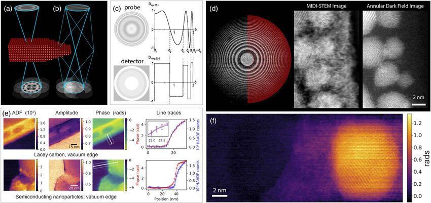
568                                                                                                                                                              Colin Ophus

          of the experimental parameters and dose in order to measure                                    4D-STEM strain measurements have an inherent trade-off
          structural properties such as orientation to the required precision,                       between resolution in real space and reciprocal space. A larger con-
          balanced against the density of probe positions. For a review of                           vergence angle will generate a smaller probe, giving better resolu-
          electron beam damage mechanisms and how they can be mini-                                  tion in real space. However, this will also decrease the strain
          mized, we direct readers to Egerton (2019).                                                measurement precision. By decreasing the convergence angle, the
                                                                                                     STEM probe size in real space will be increased. A 4D-STEM mea-
                                                                                                     surement under these conditions will have lower spatial resolution
          Strain Mapping
                                                                                                     but improved strain precision, due to averaging the strain measure-
          Many functional materials possess a large degree of local variation                        ment over a larger volume. However, the STEM probes can also
          in lattice parameter (or for amorphous or semicrystalline materi-                          be spaced further apart than the spatial resolution limit. Thus
          als, variation in local atomic spacing), which can have a large effect                     the only limit on FOV size is the speed of the detector readout.
          on the materials’ electronic and mechanical properties. TEM can                            By using the millisecond readout times possible with direct elec-
          measure these local strains with both good precision and high res-                         tron detectors, the FOV can be increased as demonstrated by
          olution using CBED patterns, NBED, HRTEM, and dark field                                   Müller et al. (2012b). Another example of the large FOV possible
          holography (Hÿtch & Minor, 2014). Strain measurements with                                 with 4D-STEM strain measurements is plotted in Figure 4d, by
          CBED (or large angle CBED, i.e., LACBED) usually refers to                                 Ozdol et al. (2015). In this work, the sample region scanned was
          using precision measurements of the higher order Laue zone                                 almost 1 µm2, and the measurement was found to be extremely
          (HOLZ) features of the diffraction pattern of a converged electron                         consistent across the FOV for a well-controlled multilayer semicon-
          probe to directly probe the local lattice parameter (Jones et al.,                         ductor sample. 4D-STEM strain measurements have also been per-
          1977). While in principle this is compatible with 4D-STEM mea-                             formed in situ, for example in Pekin et al. (2018).
          surements, these measurements typically require detailed calcula-                              One notable extension to NBED strain measurements in
          tions to interpret the CBED patterns (Rozeveld & Howe, 1993),                              4D-STEM is the use of PED to enhance the measurement preci-
          samples thin enough for the kinematic approximation to hold                                sion. Heterogeneity in the diffraction disks is typically the limiting
          (Zuo, 1992), and usually a favorable symmetry of the CBED pat-                             factor in the measurement precision, for example as shown in
          tern along the available sample orientations (Kaufman et al.,                              measurements by Pekin et al. (2017). PED can improve precision
          1986). Nevertheless, CBED HOLZ measurements of local strain                                of 4D-STEM strain measurements, shown by Rouviere et al.
          are widely used, especially for single crystalline semiconductor                           (2013), Vigouroux et al. (2014), and Reisinger et al. (2016) for
          samples such as in Clément et al. (2004) or Zhang et al. (2006).                           multilayer semiconductor devices. The improvement in precision
              In contrast, strain measurements from NBED experiments are                             for PED strain measurements was also analyzed in detail by Mahr
          usually simpler to interpret. Because the local strain precision does                      et al. (2015). PED was also used to measure strain maps for com-
          not depend on directly measuring the atomic column positions,                              plex polycrystalline materials by Rottmann & Hemker (2018),
          the FOV is essentially unlimited and almost any sample and orienta-                        including high precision measurements of strain in low angle
          tion can be used (Béché et al., 2009). A schematic of an NBED strain                       grain boundaries and even single dislocations. These experiments
          measurement is shown in Figure 4a, illustrating the inverse relation-                      are shown in Figure 4e. Mahr et al. (2015) also proposed the use
          ship between interatomic distance and diffraction disk spacing.                            of a patterned probe-forming aperture to improve strain measure-
              The NBED strain measurement technique was first introduced                             ment precision, specifically the addition of a cross which divides
          by Usuda et al. (2004), applied to the sample shown in Figure 4b.                          the probe into four quarters. Guzzinati et al. (2019) have also used
          To improve the spatial resolution of the strain measurements, the                          a patterned annular ring aperture to generate Bessel beam STEM
          STEM probe size must be decreased by opening up the conver-                                probes, which improves the measure of strain precision.
          gence semiangle of the probe-forming aperture in diffraction                                   In addition to crystalline materials, amorphous and semi-
          space. This however will introduce unwanted fine structure con-                            crystalline materials can also exhibit local deviations away from
          trast in the diffraction disks for thicker samples, due to excitation                      the mean atomic spacing or average layer stacking distance respec-
          errors and dynamical diffraction, shown in experiments by Müller                           tively. Ebner et al. (2016) demonstrated that it was possible to
          et al. (2012a) and plotted in Figure 4c. In that study, the authors                        measure this variation in a metallic glass. By combining this
          focused on making their measurements as accurate and robust as                             method with 4D-STEM performed with a fast detector,
          possible for the large variation in the diffraction disk intensity                         Gammer et al. (2018) were able to map the strain distribution
          patterns, using circular pattern recognition. This was also the                            in a metallic glass sample machined into a dogbone geometry
          focus of the work by Pekin et al. (2017), who analyzed using dif-                          for in-situ mechanical testing. Figure 4f shows an intermediate
          ferent correlation methods where a vacuum reference probe was                              time step where the sample is under mechanical load; the mean
          compared with experimental and synthetic diffraction patterns.                             CBED image shows the characteristic “amorphous ring” which
          Other authors have analyzed the accuracy of NBED strain mea-                               was fit for every probe position to determine the relative strain
          surements including Williamson et al. (2015), Grieb et al.                                 maps, referenced to the unloaded sample.
          (2017), and Grieb et al. (2018), or the influence of artifacts such                            Finally we note that alternative detector technologies have also
          as elliptic distortion by Mahr et al. (2019).                                              been employed to measure strain maps. For example, Müller-
              Many researchers have applied NBED to materials science stud-                          Caspary et al. (2015) used a delay-line detector to map strain in
          ies, including Liu et al. (2008), Sourty et al. (2009), Favia et al.                       field effect transistors fabricated from silicon.
          (2010), Uesugi et al. (2011), and Haas et al. (2017). Very recent
          studies, including Han et al. (2018), have even extended strain mea-
                                                                                                     Medium Range Order Measurement Using Fluctuation
          surements to heterostructures in very weakly scattering 2D materi-
                                                                                                     Electron Microscopy
          als. Comparisons of the strengths and weaknesses between NBED
          and other TEM strain measurement methods have been performed                               Many interesting materials in materials science are not crystalline,
          by Favia et al. (2011) and Cooper et al. (2016).                                           and the tendency of some materials to form structurally disordered

Downloaded from https://www.cambridge.org/core. IP address: 46.4.80.155, on 21 Jan 2022 at 12:30:25, subject to the Cambridge Core terms of use, available at https://www.cambridge.org/core/terms.
https://doi.org/10.1017/S1431927619000497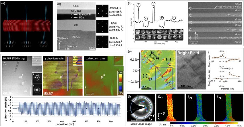
Microscopy and Microanalysis                                                                                                                                                 569

           Fig. 4. Strain measurements in 4D-STEM. a: Schematic showing how diffraction disk spacing varies inversely with interatomic distances. b: Precise lattice parameter
           determination in multilayer semiconductor sample, from Usuda et al. (2004). c: Strain measurements in the presence of large variations of diffraction disk contrast
           patterns, adapted from Müller et al. (2012a). d: Strain maps with a large FOV, from Ozdol et al. (2015). e: Strain map from a polycrystalline sample, with strain
           distributions of single distributions plotted, from Rottmann & Hemker (2018). f: Strain measurements from a metallic glass mechanical testing sample, adapted
           from Gammer et al. (2018).

           or “glassy” phases has been discussed for a long time (Phillips,                           length scale and density of all rotational orders up to 12-fold sym-
           1979). The degree of medium range order (MRO) in glassy mate-                              metry. By comparing these measurements with atomic models,
           rials can be measured using “fluctuation electron microscopy”                              they concluded that icosahedral ordering was the dominant struc-
           (FEM), as suggested by Treacy & Gibson (1996) and drawn sche-                              tural motif due to strong measurements of two, six, and tenfold
           matically in Figure 5a. Figure 5b shows FEM measurements of                                symmetries. Figure 5e also shows spatial maps of these features.
           α-Ge performed using converged electron probes, shown by                                   A follow up study by Liu et al. (2015) used simulations to test
           Rodenburg (1999). This experiment demonstrates the basic princi-                           the interpretation of angular cross-correlation functions. Pekin
           ple of FEM: when the probe is focused to roughly the same length                           et al. (2018) have extended this method to in-situ heating exper-
           scale as the atomic ordering length of the sample, “speckles”                              iments for a Cu–Zr–Al metallic glass, and Im et al. (2018) have
           appear in the diffraction pattern. When the probe is defocused                             measured the degree of local ordering for different angular
           (made larger in the sample plane), these speckles fade away.                               symmetries in a Zr–Co–Al glass, both using modern 4D-STEM
           Measuring the intensity variance as a function of scattering                               cameras capable of recording a large amount of data with good
           angle (e.g., the ring shown in Fig. 5b) and probe size can yield                           statistics. A review of TEM measurements of heterogeneity in
           information about the degree of MRO and the length scales                                  metallic glasses has been published by Tian & Volkert (2018).
           where it is present in a sample. Voyles & Muller (2002) showed
           that STEM has significant measurement advantages over other
                                                                                                      Position-Averaged Convergent Beam Electron Diffraction
           TEM operating modes for FEM, one being the ability to easily
           adjust the probe size, for “variable resolution” (VR)-FEM. Some                            Quantitative CBED has a long history in TEM research, since
           of their FEM measurements of α-Si are shown in Figure 5c. By                               under the right imaging conditions various sample parameters
           using VR-FEM, the characteristic length scale of the MRO can                               such as thickness can be determined with high precision (Steeds,
           be determined, such as in the example plotted in Figure 5d from                            1979). However, conventional CBED experiments can require pre-
           Bogle et al. (2010). VR-FEM has been used to study many other                              cise tilting of the sample, a minimum sample thickness to be effec-
           materials, for example metallic glasses in Hwang et al. (2012)                             tive, and sometimes require simulations to interpret the results. A
           and α-Si in Hilke et al. (2019).                                                           recent related diffraction imaging method was introduced by
               A large amount of scattering information is collected when                             LeBeau et al. (2009), called position-averaged convergent beam
           performing a 4D-STEM FEM experiment. In addition to estimat-                               electron diffraction (PACBED). In this technique, shown schemati-
           ing the degree of MRO, it can also be used to measure the density                          cally in Figure 6a, the diffraction patterns of an atomic-scale (large
           of atomic clusters with different rotational symmetry. Examples of                         convergence angle) probe are incoherently averaged as the beam is
           diffraction images of individual atomic clusters are shown in                              scanned over the sample surface. As long as the averaging is per-
           (Hirata et al., 2011). Figure 5e shows a measurement of Cu–Zr                              formed over at least one full unit cell of a crystalline sample,
           metallic glass where Liu et al. (2013) used angular cross-                                 PACBED images form a fingerprint signal, which can be used to
           correlation functions of the diffraction patterns to measure the                           determine sample parameters such as thickness, tilt, or sample

Downloaded from https://www.cambridge.org/core. IP address: 46.4.80.155, on 21 Jan 2022 at 12:30:25, subject to the Cambridge Core terms of use, available at https://www.cambridge.org/core/terms.
https://doi.org/10.1017/S1431927619000497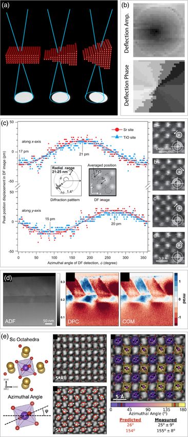
570 Colin Ophus
Fig. 5. FEM in STEM. a: Schematic showing how structural disorder generates the speckle pattern used in FEM. b: FEM measurements of α-Ge, adapted from
Rodenburg (1999). c: FEM measurements of α-Si using a variable STEM probe size, from Voyles & Muller (2002). d: Characteristic length scale measurements of
MRO in α-Si, from Bogle et al. (2010). e: Example of diffraction patterns of a Cu–Zr metallic glass, measurement of local MRO symmetry using angular cross-
correlation functions, adapted from Liu et al. (2013).
polarization with high precision, by comparing directly with HAADF is not very sensitive to weakly scattering samples such as
simulated PACBED images, as shown by LeBeau et al. (2010). low atomic number materials or 2D materials (Ophus et al.,
Figure 6b shows one of their experiments, thickness determination 2016). A more dose-efficient alternative is phase contrast imaging,
of a PbWO4 sample over a large range of sample thicknesses, using which is therefore more suitable for these cases. Methods for mea-
comparisons with Bloch wave simulations. PACBED thickness suring the phase shift imparted to an electron wave by a sample in
measurements have found widespread application in STEM exper- a STEM experiment were first discussed by Rose (1974), Dekkers
iments, for example in Zhu et al. (2012), Hwang et al. (2013), and De Lang (1974), and Rose (1977). These STEM phase con-
Yankovich et al. (2014), and Grimley et al. (2018). trast imaging methods and some modern 4D-STEM extensions
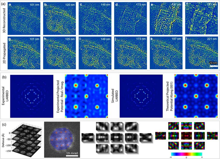
Ophus et al. (2014) showed that 4D-STEM datasets of crystal- will be discussed in this section.
line samples can be adapted to form PACBED images. First, the
lattice is fit to either a simultaneously recorded ADF image, or
Differential Phase Contrast
a virtual image from the 4D-STEM dataset, and then each
probe is assigned to a given unit cell. Averaging these patterns When a converged electron probe has a similar size to the length
produces a single unit cell-scale PACBED image. An example of scale of the variations of a sample’s electric field (gradient of the
this procedure is shown in Figure 6c, where PACBED was used electrostatic potential), it will be partially or wholly deflected.
to determine the local composition of a LaMnO2–SrTiO3 multi- Figure 7a shows an ideal probe deflection in the presence of a
layer stack in a STEM instrument without aberration correction, phase gradient with infinite extent. This momentum change
from Ophus et al. (2017a). Note that as seen in the HAADF imparted to the STEM probe can be measured in diffraction
images, the STEM probe resolution was not sufficient to resolve space using a variety of detector configurations, originally by
individual atomic columns inside the perovskite unit cell, showing using a difference signal between different segmented detectors
that PACBED does not require high resolution STEM imaging. that do not have rotational symmetry (Dekkers & De Lang,
PACBED has also been used to measure unit cell distortion in 1974), a method long known in optical microscopy (Françon,
double-unit-cell perovskites by Nord et al. (2018). A recently 1954). The differential phase contrast (DPC) imaging technique
developed method to augment PACBED fitting was shown by implemented on segmented detectors (Haider et al., 1994) was
Xu & LeBeau (2018), who used a convolutional neural network steadily improved all the way to atomic resolution imaging
to automatically align and analyze the images. They showed (Shibata et al., 2012). More information on the theory of DPC
that this approach can be quite robust to noise and can process can be found in Lubk & Zweck (2015). Note that in Lorentz imag-
PACBED images very quickly, which is important since the data- ing modes in TEM, DPC measurements are also sensitive to the
set sizes can be very large. magnetic field of the sample (Chapman et al., 1990).
As discussed by Waddell & Chapman (1979), Pennycook et al.
(2015), and Yang et al. (2015b), use of fixed segmented detectors
Phase Contrast Imaging
for DPC measurements reduces the information transfer effi-
As described above, the most popular STEM imaging method for ciency of many spatial frequencies. One way to avoid this problem
samples in materials science is HAADF measurements. However, is to perform a full 4D-STEM scan using a pixelated detector, and
Downloaded from https://www.cambridge.org/core. IP address: 46.4.80.155, on 21 Jan 2022 at 12:30:25, subject to the Cambridge Core terms of use, available at https://www.cambridge.org/core/terms.
https://doi.org/10.1017/S1431927619000497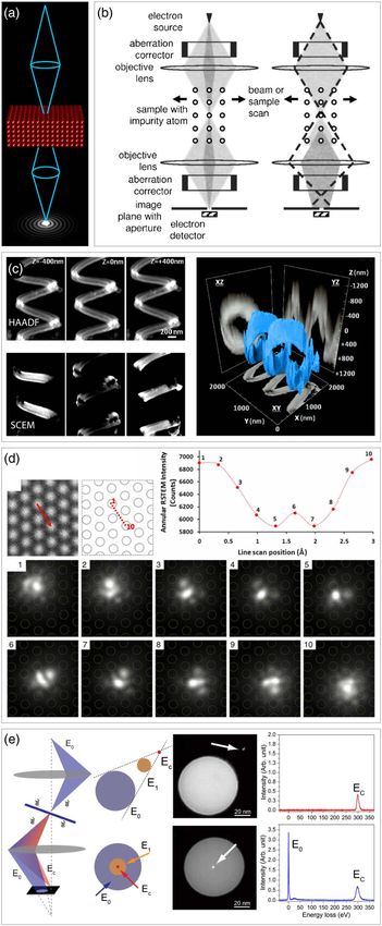
Microscopy and Microanalysis                                                                                                                                                 571

           Fig. 6. Position averaged convergent beam electron diffraction (PACBED). a: Schematic showing how thickness strongly modules PACBED images. b: Thickness
           fitting of PbWO4 using PACBED, adapted from LeBeau et al. (2010). c: Composition fitting of LaMnO3–SrTiO3 multilayers using PACBED, adapted from Ophus
           et al. (2017a).

           measuring the momentum change of the electron probe using a                                probe to a very small number of variables such as the COM dis-
           “center of mass” (COM) measurement over all pixels. Müller-                                placement vector. This allows fast alternatives to pixelated detectors
           Caspary et al. (2017) calculated that approximately 10 × 10 detector                       to be used for DPC measurements, such as the previously men-
           pixels were sufficient for COM DPC measurements, though more                               tioned segmented or delay-line detectors, or a duo-lateral position
           pixels may be desired for redundancy, or to perform additional                             sensitive diode detector which can read out the COM of the probe
           simultaneous measurements such as HAADF imaging. They have                                 as opposed to a full image, such as in Schwarzhuber et al. (2018).
           also published a follow up study in Müller-Caspary et al. (2018b)                          It may also be possible to use pixelated 4D-STEM detectors in
           to directly compare COM DPC with segmented detector DPC.                                   combination with dedicated hardware directly after the detector
           Quantitative DPC can also be used for thicker samples if a large                           pixels such as a field-programmable gate array, to perform simple
           probe-forming aperture is combined with segmented detectors                                measurements such as DPC (Johnson et al., 2018). This would
           aligned with the edge of the probe as shown by Brown et al. (2019).                        remove the necessity of transferring, storing, and processing
               An early 4D-STEM DPC measurement of the Lorentz field                                  the full 4D-STEM datasets, which can be very large. A speed
           deflection of a permalloy microdot by Zaluzec (2002) is plotted                            up in DPC inversion can also be accomplished computationally,
           in Figure 7b. One of the first 4D-STEM measurements which                                  as in Brown et al. (2016).
           measured the deflection of the STEM probe around atomic col-
           umns in SrTiO3 was performed by Kimoto & Ishizuka (2011).
                                                                                                      Ptychography
           These (x,y) STEM probe displacements around columns of Sr
           and Ti–O are plotted in Figure 7c. Since then, 4D-STEM DPC                                 The DPC experiments described in the previous section reduce
           has been applied to various materials science problems. Some                               the measurement performed at each probe position to a two ele-
           atomic-resolution examples include imaging of SrTiO3 by                                    ment vector corresponding to the mean change of the electron
           Müller et al. (2014), imaging of GaN and graphene by Lazić                                 probe’s momentum due to gradients in the sample potential.
           et al. (2016), and imaging of SrTiO3 and MoS2 by Chen et al.                               This is an intuitive and useful way to understand the beam–
           (2016). Figure 7d shows a 4D-STEM DPC measurement of a mul-                                sample interactions due to elastic scattering in STEM, but discards
           tilayer BiFeO3/SrRuO3/DyScO3 stack performed by Tate et al.                                a significant amount of information about the sample. This is
           (2016). Hachtel et al. (2018) measured octahedral tilts in the dis-                        because for thin specimens, STEM is essentially a convolution
           torted perovskite DyScO3, which are plotted in Figure 7e. These                            of the electron probe with the projected potential of a sample.
           and other literature examples such as Krajnak et al. (2016),                               By recording the full STEM probe diffraction pattern, we are
           Nord et al. (2016), and Müller-Caspary et al. (2018a) show that                            measuring the degree of scattering for many different spatial fre-
           4D-STEM DPC is becoming a widespread tool for easy phase                                   quencies of the sample’s projected potential. Combining many
           contrast measurements in STEM over a large range of length                                 such overlapping measurements such as the 4D-STEM experi-
           scales. Yadav et al. (2019) have recently shown that in addition                           ment shown in Figure 8a, we can use computational methods
           to the local electric field, the local polarization can be measured                        to reconstruct both the complex electron probe and complex sam-
           simultaneously using 4D-STEM.                                                              ple potential with high accuracy. Hegerl & Hoppe (1970) coined
               One advantage of DPC relative to more complex 4D-STEM                                  the name “ptychography” for this class of methods. The heart of
           measurements is that it reduces the measurement data of each                               this method was described in a series of papers, Hoppe (1969a),

Downloaded from https://www.cambridge.org/core. IP address: 46.4.80.155, on 21 Jan 2022 at 12:30:25, subject to the Cambridge Core terms of use, available at https://www.cambridge.org/core/terms.
https://doi.org/10.1017/S1431927619000497
572 Colin Ophus
diffraction images also shown in Figure 8b demonstrate the
high sensitivity of diffraction images to the local alignment of
the probe with respect to an underlying lattice.
Over the next two decades, a few theoretical studies of ptychog-
raphy were published including Hawkes (1982) and Konnert &
D’Antonio (1986), and also some experimental scanning microdif-
fraction studies including Cowley (1984) and Cowley & Ou (1989).
However, the first reconstruction method for ptychography similar
to modern methods has not been published to date (Bates &
Rodenburg, 1989). These authors later published a substantially
improved reconstruction method in Rodenburg & Bates (1992),
the Wigner-distribution deconvolution (WDD) method which is
still in use today for electron ptychography. Also suggested in
that paper was the use of iterative methods for ptychography,
examples of which were published in Faulkner & Rodenburg
(2004), Rodenburg & Faulkner (2004), Maiden & Rodenburg
(2009), and other studies. Another nonlinear approach to ptycho-
graphic reconstruction was proposed by D’alfonso et al. (2014).
Early experimental demonstrations of the principles of pty-
chography were published by Rodenburg et al. (1993), and the
first experiment which imaged past the conventional TEM infor-
mation limit using ptychography was published by Nellist et al.
(1995). This result, shown in Figure 8d, reconstructed the struc-
ture factors for a small number of diffraction vectors, a method
which requires a periodic sample. Iterative ptychography in
TEM experiments that used information contained inside the
STEM probe BF disk was shown by Hüe et al. (2010), and shortly
thereafter Putkunz et al. (2012) demonstrated atomic-scale
ptychography by imaging boron nanocones. In the same year,
ptychographic reconstructions that used the electron intensity
scattered beyond the probe-forming angular range were published
by Humphry et al. (2012), reproduced in Figure 8e.
Using 4D-STEM experiments and a non-iterative “single-side
band” reconstruction method, atomic resolution ptychography
reconstructions of bilayer graphene were shown by Pennycook
et al. (2015), and are plotted in Figure 8c. This work was followed
by a theoretical paper by Yang et al. (2015b) which derived the
optimum imaging conditions for focused probe ptychography
and analyzed the advantages of using 4D-STEM over segmented
detectors. This same group also used WDD ptychography and con-
ventional imaging modes to analyze complex nanostructures in
Yang et al. (2016b), shown in Figure 8f. To date, the highest reso-
lution 4D-STEM ptychography experiments have been performed
by Jiang et al. (2018). These experiments imaged bilayer MoS2,
plotted in Figure 8g. This paper estimated a resolution of 0.39 Å
using an electron voltage of 80 kV, significantly beyond the conven-
tional imaging resolution of 0.98 Å for these microscope parame-
ters. Additionally, this paper also used simulations to determine
that defocused-probe iterative ptychography outperformed both
focused-probe iterative ptychography and the WDD reconstruction
Fig. 7. DPC measurements in STEM. a: STEM probe deflection from ideal phase method by approximately a factor of 2 for signal-to-noise. Various
wedges with different slopes. b: Lorentz field deflection measurement of a permalloy authors have applied ptychography to solve materials science ques-
microdot, adapted from Zaluzec (2002). c: Shift of peak positions in SrTiO3, from
tions, including Yang et al. (2015a, 2017), Wang et al. (2017), dos
Kimoto & Ishizuka (2011). d: Simultaneous measurements of ADF image, DPC signal
from segments, and COM DPC signal from a multilayer stack, adapted from Tate et al. Reis et al. (2018), Lozano et al. (2018), and Fang et al. (2019).
(2016). e: DPC measurements of octahedral tilts in DyScO3, from Hachtel et al. (2018). An interesting expansion of ptychography is the use of “hol-
low” diffraction patterns, whereby the 4D-STEM detector has a
hole drilled in the center to allow for part or all of the unscattered
Hoppe & Strube (1969), and Hoppe (1969b). Figure 8b shows the electron beam to pass through into a spectrometer. Song et al.
essential idea of ptychography, where at different electron probe (2018) showed that even with part of the measurement signal
positions, there is substantial overlap in the illuminated regions. removed, atomic-resolution phase signals can still be recon-
The differing intensities in these overlapping regions can be structed. This “hollow” detector configuration is compatible with
used to solve for the phase of the electron exit wave. The lattice a large number of 4D-STEM techniques discussed in this paper
Downloaded from https://www.cambridge.org/core. IP address: 46.4.80.155, on 21 Jan 2022 at 12:30:25, subject to the Cambridge Core terms of use, available at https://www.cambridge.org/core/terms.
https://doi.org/10.1017/S1431927619000497Microscopy and Microanalysis 573
Fig. 8. Electron ptychography. a: Experimental geometry showing how overlapping probes (either converged or defocused) can be used to solve the exit wave
phase. b: (Left) Schematic of convolution of square lattice with circular and rectangular probes with overlapping regions shaded, from Hoppe (1969a). Optical
interference between diffraction of square lattice with circular hole when (center) aligned to lattice point, and (right) aligned to center of four lattice points,
from Hoppe & Strube (1969). c: Ptychographic reconstruction of twisted bilayer graphene, from Pennycook et al. (2015). d: Reconstruction of periodic silicon lattice,
from Nellist et al. (1995). e: Atomic-resolution ptychographic imaging of aperiodic samples in a modified SEM, adapted from Humphry et al. (2012), with
contrast-enhanced inset. f: Simultaneous imaging modes including WDD ptychography of double-walled nanotube containing carbon nanostructures and iodine
atoms, from Yang et al. (2016b). g: Ptychographic reconstruction of twisted bilayer MoS2 which resolves 0.4 Å Mo dumbbells, from Jiang et al. (2018).
and we expect it to find widespread use once dedicated “hollow” independently. By measuring the difference signal between the 0
pixelated STEM detectors are widely available. and π/2 zones, the local sample phase can be measured directly
Ptychography is a computational imaging method; thus in with a weighted detector such as that shown in Figure 9c. This
addition to benefiting from hardware such as aberration correc- method is essentially an extension of the ABF measurement method
tion or better 4D-STEM detectors, algorithmic improvements described above (Findlay et al., 2010). However, using the probe
are also possible. Some promising research avenues for electron defocus and spherical aberration limits how many difference zones
ptychography have been explored in Thibault & Menzel (2013), can be used, and using annular ring detectors requires very precise
Pelz et al. (2017), and other studies. Some authors have also and stable alignment of the probe with respect to the detectors.
explored expanding ptychography to a 3D technique by using a This phase contrast measurement technique was recently
multislice method, including Gao et al. (2017). Others are making updated in two ways: first by using a phase plate to produce the
use of the redundancy in 4D-STEM ptychographic measurements desired probe illumination where 50% of the probe in reciprocal
to apply ideas from the field of compressed sensing in order to space is phase shifted by π/2 rad, while the remaining regions
reduce the number of required measurements, such as the study are not phase shifted (note the shape of these zones does not mat-
by Stevens et al. (2018). ter), an experimental geometry shown in Figure 9a. Second, a pix-
elated electron detector is used to measure the transmitted probes
in diffraction space (i.e., a 4D-STEM measurement), where a virtual
Phase Structured Electron Probes
detector can then be exactly matched to the phase plate pattern.
Both DPC and ptychography rely on overlapping adjacent STEM This method was termed “matched illumination and detector
probes to create enough redundant information for the phase of interferometry” (MIDI)-STEM, demonstrated experimentally at
the object wave to be reconstructed. Alternatives to lateral-shift or atomic resolution by Ophus et al. (2016), shown in Figure 9d.
COM DPC were also discussed in the work by Rose (1974). Rose MIDI-STEM produces contrast with significantly less high-pass
derived that the ideal detector for measuring phase contrast from filtering than DPC or ptychography, but is less efficient at higher
radially symmetric STEM probes is a difference signal between alter- spatial frequencies. Interestingly, combining MIDI-STEM with
nating radially symmetric “zones” aligned with the oscillations in ptychography produces additional contrast making it more effi-
the STEM probe’s contrast transfer function, a concept further cient than either method used alone (Yang et al., 2016a). The
developed by Hammel & Rose (1995). The combination of defocus use of MIDI-STEM for optical sectioning was recently investigated
and spherical aberration can produce a STEM probe with a known by Lee et al. (2019), who refer to this technique (without a material
contrast transfer function which is divided into regions of approxi- phase plate) as annular differential phase contrast.
mately 0 and π/2 rad phase shift, as shown in Figure 9c. These alter- Each of the previously discussed methods for phase contrast
nating zones are matched to multiple annular detector rings, where imaging in 4D-STEM applies high-pass filtering of the phase sig-
the probe intensity incident onto each ring is measured nal of the sample to some degree. This limits the ability to use
Downloaded from https://www.cambridge.org/core. IP address: 46.4.80.155, on 21 Jan 2022 at 12:30:25, subject to the Cambridge Core terms of use, available at https://www.cambridge.org/core/terms.
https://doi.org/10.1017/S1431927619000497You can also read