Fanless, porous graphene copper composite heat sink for micro devices
←
→
Page content transcription
If your browser does not render page correctly, please read the page content below
www.nature.com/scientificreports
OPEN Fanless, porous graphene‑copper
composite heat sink for micro
devices
Hokyun Rho1, Yea Sol Jang2, Hyojung Bae1, An‑Na Cha1, Sang Hyun Lee1* & Jun‑Seok Ha1*
Thermal management in devices directly affects their performance, but it is difficult to apply
conventional cooling methods such as the use of cooling liquids or fans to micro devices owing to the
small size of micro devices. In this study, we attempted to solve this problem by employing a heat sink
fabricated using copper with porous structures consisting of single-layer graphene on the surface and
graphene oxide inside the pores. The porous copper/single-layer graphene/graphene oxide composite
(p-Cu/G/rGO) had a porosity of approximately 35%, and the measured pore size was approximately
10 to 100 µm. The internal GO was reduced at a temperature of 1000 °C. On observing the heat
distribution in the structure using a thermal imaging camera, we could observe that the p-Cu/G/rGO
was conducting heat faster than the p-Cu, which was consistent with the simulation. Furthermore,
the thermal resistance of p-Cu/G/rGO was lower than those of the p-Cu and pure Cu. When the p-Cu/G/
rGO was fabricated into a heat sink to mount the light emitting diode (LED) chip, the measured
temperature of the LED was 31.04 °C, which was less than the temperature of the pure Cu of 40.8 °C.
After a week of being subjected to high power (1000 mA), the light intensity of p-Cu/G/rGO decreased
to 95.24%. However, the pure Cu decreased significantly to 66.04%. The results of this study are
expected to be applied to micro devices for their effective thermal management.
The thermal management of micro devices has become increasingly important as the internal density of their
circuits has increased1–3. As the aggregation of the internal circuits in electronic devices has increased, the amount
of current per unit area has increased significantly4–6. The heat generated by an electronic device shortens the
lifetime of that device or causes the occurrence of a f ailure7–10. According to the Arrhenius equation, the lifespan
of an electronic device is cut in half when its temperature increases by 10 °C11,12. Therefore, it is necessary to
develop heat sinks that can immediately release the heat generated by electronic devices. One of the properties
required for effective thermal management with heat sink in electronic devices is heat dissipation properties. If
the heat dissipation of heat sink is low, the temperature will rise due to continuous heat supply, and the device
will be damaged13–15. Fans are used to improve the heat dissipation of heat sinks. However, it is difficult to attach
fans to micro devices owing to the large volume, additional power requirement, and noise generation of fans.
The development of a fanless heat sink is a challenge for future thermal management. A high heat dissipation is
required in the case of a fanless heat sink, and a wide surface area and radiation rate are required for realizing
a high heat dissipation16–18. Therefore, structures comprising a wide surface area, such as porous structures,
are advantageous, and the use of materials having a high radiation rate is one solution to the aforementioned
problem. Another well-known requirement of heat sinks is their high thermal conductivity19–21. Traditionally,
primarily metals, which have a high heat conductivity, were used in heat sinks, but a significant amount of
research was conducted to realize a higher heat conductivity by adding fillers to the metals22–26. Graphene, carbon
nanotubes, fullerene, and diamond, which are carbon materials that have a high thermal conductivity, have been
widely studied for such a pplications26–28. In particular, graphene has a very high thermal conductivity of 4000 W/
mk. However, the range of improvements that can be realized in the characteristics of the actual heat dissipation
material is small, because the ratio of the total density is low and the aspect ratio of the heat conductivity is large
owing to its stratified s tructure29–31.
In this study, p-Cu/G/rGO was manufactured using copper powder, graphene oxide, and single-layer gra-
phene surrounding the copper surface. The composite was identified as a porous structure having a porosity
of approximately 35%. Single-layer graphene was synthesized on the surface of copper, and the GO inside was
reduced at 1000 °C. The thermal conductivity of p-Cu/G/rGO was higher than that of p-Cu, and the temperature
distribution analysis performed using a thermal imaging camera showed the same result as the simulation. The
1
Chonnam National University, Gwangju 61186, South Korea. 2Korea Electronics Technology Institute,
Seongnam‑si, Gyeonggi‑do 13509, South Korea. *email: leeshyun@chonnam.ac.kr; jsha@jnu.ac.kr
Scientific Reports | (2021) 11:17607 | https://doi.org/10.1038/s41598-021-97165-y 1
Vol.:(0123456789)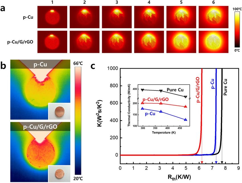
www.nature.com/scientificreports/
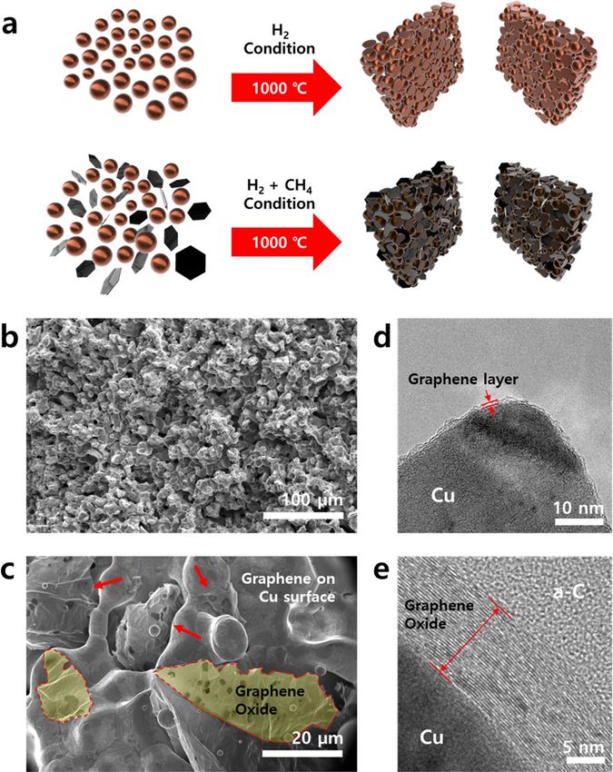
Figure 1. Schematic of a method for synthesizing p-Cu/G/rGO (a). SEM image of the internal structure of the
p-Cu/G/rGO (b,c). TEM analysis of graphene and graphene oxide formed on a porous copper surface (d,e).
composite was fabricated into a heat sink that was used to mount the light emitting diode (LED), and the thermal
management characteristics of the composite were analyzed.
Result and discussion
Copper powder of 5-μm particle size and graphene oxide were mixed and placed in a boat of 15 × 40 mm for
synthesizing the graphene by thermal chemical vapor deposition. In order to confirm the structural character-
istics, the surface of the composite was observed using scanning electron microscopy (SEM). The results are
shown in Fig. 1. The observed p-Cu/G/rGO comprised a porous structure with graphene oxide inside its pores.
Transmission electron microscopy (TEM) was used to observe the surface in greater detail. A single layer of
graphene was formed on the surface of the copper, and it was also found that the graphene oxide was attached to
the copper. This structure was created as follows. A 5-µm-sized copper powder was welded to the other copper
powders around it, with the surface melted at a temperature of 1000 °C to form a porous structure. The surface
melted at 1000 °C, below the melting point of copper, i.e., 1024 °C, owing to the lack of an outermost copper
bond. The copper surface, which lacks atomic coupling, becomes unstable and melts at a temperature lower than
its melting p oint32,33. This causes only the surface of the copper powder to be welded and a porous structure to
form. At this time, the graphene oxide desorbs oxygen at the defect site owing to the temperature of 1000 °C and
is reduced to graphene34–36. The reduced graphene oxides are bonded to a liquid copper surface. When methane is
Scientific Reports | (2021) 11:17607 | https://doi.org/10.1038/s41598-021-97165-y 2
Vol:.(1234567890)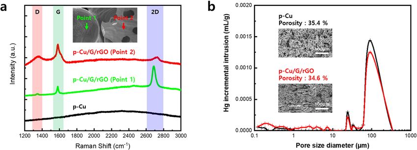
www.nature.com/scientificreports/
Figure 2. Raman spectroscopy of graphene and graphene oxide portions on copper surfaces (a). BET analysis
for internal porosity and pore size confirmation (b).
injected, the carbon atoms are then separated and dissolved in the porous copper at 1000 °C. In the cooling step,
the carbon precipitates to grow into graphene on the surface of the copper and connects the reduced graphene
oxide to result in a three-dimensionally connected graphene s hape37–39.
The prepared p-Cu/G/rGO was analyzed using Raman spectroscopy and is shown in Fig. 2. The parts that
appeared to be copper and those that appeared to be reduced graphene oxide were measured respectively, and
the porous copper samples produced using only copper powder were also compared. In Raman spectroscopy,
graphene is usually identified by peaks called D(~ 1350 cm−1), G(~ 1580 cm−1), and 2D(~ 2690 cm−1). The D-peak
is caused by disordered oscillation in sp2 bonds (generally a defect), and the G peak arises from the stretching
of the C–C bond in graphitic materials and is common to all sp2 carbon systems. The 2D-peak is caused by a
second-order two-phonon process. In addition, the intensity comparison of the G-peak and 2D-peak provides
information regarding the number of graphene l ayers40–43. In the part that appears to be copper, the ratio of the
G and 2D peaks is approximately 1:3, and it seems that a single layer of graphene exists. In the part that appears
to be graphene oxide, the intensity of the G-peak is very high as compared to that of the 2D peak, and thus, the
graphene oxide is considered to be reduced. Compared to the single-layer graphene, the 2D peak position of the
reduced graphene oxide is shifted owing to their structural differences. The peaks of the reduced graphene oxide
may not perfectly match those of the single-layer graphene owing to the up-and-down interference caused by
the multi-layer structure and irregular atomic behavior due to several defects. No peaks were observed for the
p-Cu samples prepared using only copper powder. The porosity of the porous structure was measured via BET
(Brunauer–Emmett–Teller) analysis. The porosity was approximately 34.6%, and pores of approximately 10 to
100 µm in size were measured. In order for convection to occur within the open pores, the pore diameter should
be 10 times the air’s mean free path (MFP)44,45. In other words, the MFP of the air is approximately 64 nm, and
heat exchange is thus possible if the pore diameter is greater than 640 nm.
A simulation was performed to confirm the heat dissipation ability of p-Cu/G/rGO, and is shown in Fig. 3a.
The heating source was placed on top of the p-Cu and p-Cu/G/rGO samples, and the movement of the heat
was observed by the same time step. Based on the simulation results, it can be confirmed that the heat transfer
in the p-Cu/G/rGO sample is faster than that in the p-Cu sample. This result agrees with that obtained with a
real sample (radius 10 mm × thickness 5 mm) in Fig. 3b and measured with a thermal imaging camera. Because
of their porosity, p-Cu and p-Cu/G/rGO exhibited lower thermal conductivities than that of the pure Cu. The
thermal conductivity of a material with a porosity of 35% is reduced to about 43% of that of a non-porous mate-
rial (Supporting information S3)46,47.
This value is consistent with the measured value. The thermal conductivity of all the samples decreases as
the measurement temperature increases, because of the increase in the thermal resistance due to the increased
heat. However, in the case of p-Cu/G/rGO, the thermal conductivity decrease is small because graphene is coated
onto the copper surface to prevent oxidation48–50. Furthermore, the increase in the thermal resistance due to
the heat generation was confirmed using a thermal resistance tester, and is shown in Fig. 3c. Thermal resistance
is the temperature difference across a structure when a unit of heat energy flows through it in unit time. The
measured thermal resistances of P-Cu/G/rGO p-Cu, and pure Cu were 6.20, 7.30, and 7.74 K/W, respectively,
when the incident thermal energy was 1000 W2∙s/K2. That is, for the same thermal energy, p-Cu/G/rGO had
the lowest thermal resistance. Therefore, it can be observed that it has excellent heat dissipation properties. The
reason it has a high heat dissipation property even though its thermal conductivity is lower than that of pure Cu
is because of its convection and radiation effect. The heat dissipation property is not solely influenced by thermal
conductivity but is a complex property that is affected by convection and radiation simultaneously. Irrespective
of how quickly heat is transferred from inside the heat sink, if the ability to dissipate the heat outside the heat
sink is low, the heat is accumulated in the heat sink and the temperature of the device increases. Therefore, if
the heat conductivity is above a certain value, the factors that determine the performance of the heat sink are
convection and thermal radiation. Convection and radiation are advantageous when the surface area is wide,
and since the emissivity of graphene is approximately nine times greater than that of copper, p-Cu/G/rGO has
excellent heat dissipation p roperties51–53.
We used the composite to fabricate a heat sink of dimensions 10 × 10 × 1 mm3 and mounted the LED on the
heat sink. In the temperature measurement method, 350 mA was applied for 5 min to generate heat, and the
Scientific Reports | (2021) 11:17607 | https://doi.org/10.1038/s41598-021-97165-y 3
Vol.:(0123456789)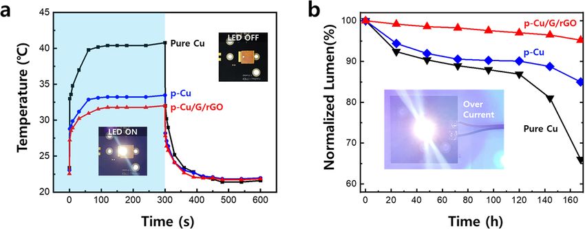
www.nature.com/scientificreports/
Figure 3. Heat transfer simulation results with and without graphene and graphene oxide in the structure (a).
Thermal imaging camera analysis to verify thermal conductivity on real samples under the same conditions as
the simulation (b). Analysis of thermal resistance (c) and thermal conductivity (inset) of composites.
Figure 4. Graph of temperature change according to on/off of LED mounted on each heat sink (a). Graph of
changes in brightness of the LEDs emitting under high power.
current was then cut off. After 5 min, the measured temperature of the LED chip was 31.04 °C, 33.48 °C, and
40.8 °C in the cases of p-Cu/G/rGO, p-Cu, and pure Cu heat sinks, respectively. This result is shown in Fig. 4a.
The hot air delivered from the surface of the heat sink moves up owing to the density difference, and cold air
is supplied from below to create natural convection. In such a case, porous structures have a large surface area
where heat exchange can occur, which is advantageous for heat dissipation. The graphene on the porous surface
makes the surface hydrophobic, thus encouraging heat exchange54. Therefore, the LEDs mounted on the p-Cu/G/
rGO can exhibit the lowest temperature. Next, the stability of the LED chip was measured and shown in Fig. 4b.
Because LEDs have a very long lifespan of approximately 50,000 h, experiments were conducted under high
power of 1000 mA, which is three times the recommended driving voltage of the corresponding LED chip. The
experiment was conducted over 1 week, and the brightness of the LEDs decreased to 95.24%, 84.99%, and 66.04%
of the original value in the cases of the p-Cu/G/rGO, p-Cu, and pure Cu heat sinks, respectively. The reason for
the sharp decrease in brightness is that the heat generated by the multi-quantum well of the LED is not emitted
and accumulates, thus causing damage to the L ED55. The p-Cu/G/rGO heat sink quickly dissipates the heat gener-
ated from the LED chip such that the heat does not accumulate at the LED, thereby resulting in a high stability.
Scientific Reports | (2021) 11:17607 | https://doi.org/10.1038/s41598-021-97165-y 4
Vol:.(1234567890)www.nature.com/scientificreports/
Conclusion
In this study, copper, graphene, and graphene oxide powders were used to produce composites with excellent
heat dissipation properties. The produced p-Cu/G/rGO composite formed a porous structure, a single layer
graphene was formed on the copper surface, and it was confirmed that reduced graphene oxide exists between
the porous structures. The p-Cu/G/rGO was confirmed to have a good heat dissipation capability owing to its
wide surface area and the presence of graphene, which was in agreement with the results of the simulation. The
temperature of the LED chip was measured by fabricating a heat sink using the p-Cu/G/rGO and mounting the
LED chip onto it. The LED mounted on the p-Cu/G/rGO heat sink exhibited the lowest temperature of 31.04 °C
and maintained a brightness of 94.24% of the original value in the LED reliability test even under severe condi-
tions. This p-Cu/G/rGO performance is expected to be incorporated into micro devices such as laptops, tablets,
and cell phones for their heat management.
Methods
p‑Cu/G/rGO manufacturing method. The copper powder having a particle size of 5 µm and the gra-
phene oxide were mixed at a weight ratio of 50:1 and placed in an aluminum-oxide boat. The temperature was
then increased to 1000 °C for 1 h in a hydrogen atmosphere. Methane was injected at a temperature of 1000 °C
and naturally cooled to room temperature after 30 min. For comparison, p-Cu was prepared only with copper
powder having a particle size of 5 µm and without the injection of methane and graphene oxide. High-purity
(99.9%) Cu was purchased from Taewon Scientific Cooperation in Korea.
Analysis of structural properties. The morphologies of the synthesized porous structures were charac-
terized using an SEM system (Nova NanoSEM 450, FEI) and a 200-kV field-emission TEM system (JEM-2100F
HR, JEOL). The graphene structure was confirmed using a Raman spectrophotometer (NRS-5100, JASCO). BET
(AutoPore IV 9500, Micromeritics) was used to confirm the pore size and porosity.
Analysis of thermal properties. The composite produced for the measurement of the thermal imaging
camera (FLIR T-335, FLIR systems, spectral range 7.5–13 μm) was processed to a diameter of 20 mm and thick-
ness of 5 mm. A heat source at 100 °C was contacted with the silver paste on top of the composite. To obtain
precise thermal properties, i.e., by preventing the occurrence of surface scattering, the surface was treated using
a commercial graphite spray (GB396352, Netzsch). The simulation was performed using the COMSOL Mul-
tiphysics software (ALTSOFT). The thermal diffusivity and specific heat were measured using the laser flash
method (LFA-457, Netzsch) and a differential scanning calorimeter (DSC 8500, Perkin Elmer) at Energy Con-
vergence Core Facility in Chonnam National University, respectively.
Analysis of LED properties. The LED chip (size 1 × 1 m
m2) used in this experiment has a vertical struc-
ture and driving current of 350 mA. The three composites (p-Cu/G/rGO, p-Cu, and pure Cu) were used to fabri-
cate heat sinks for the LED chip. The LED chip was mounted onto each heat sink using a silver paste. Aluminum-
based printed circuit boards were attached to the heat sinks. The thermal resistance of the LED device was
measured using a thermal resistance tester (T3Ster, MicReD). A lifetime test was conducted on the LED under
high power of 1000 mA and using an integrating sphere photometer (BTS256 LED Tester, Gigahertz Optik).
Received: 1 April 2021; Accepted: 3 August 2021
References
1. Wang, Q., Jiang, B., Li, B. & Yan, Y. A critical review of thermal management models and solutions of lithium-ion batteries for the
development of pure electric vehicles. Renew. Sustain. Energy Rev. 64, 106–128 (2016).
2. Kandlikar, S. G. & Hayner, C. N. Liquid cooled cold plates for industrial high-power electronic devices thermal design and manu-
facturing considerations. Heat Transf. Eng. 30, 918–930 (2009).
3. Wong, C. P. & Bollampally, R. S. Thermal conductivity, elastic modulus, and coefficient of thermal expansion of polymer composites
filled with ceramic particles for electronic packaging. J. Appl. Polym. Sci. 74, 3396–3403 (1999).
4. Dimitrakopoulos, C. D. & Malenfant, P. R. L. Organic thin film transistors for large area electronics. Adv. Mater. 14, 99–117 (2002).
5. Stoppa, M. & Chiolerio, A. Wearable electronics and smart textiles: A critical review. Sensors (Switzerland) 14, 11957–11992 (2014).
6. Matsunami, H. Technological breakthroughs in growth control of silicon carbide for high power electronic devices. Jpn. J. Appl.
Phys. 43, 6835–6847 (2004).
7. Chung, S., Lee, J. H., Jeong, J., Kim, J. J. & Hong, Y. Substrate thermal conductivity effect on heat dissipation and lifetime improve-
ment of organic light-emitting diodes. Appl. Phys. Lett. 94, 1–4 (2009).
8. Schelling, P. K., Shi, L. & Goodson, K. E. Managing heat for electronics. Mater. Today 8, 30–35 (2005).
9. Hetsroni, G., Mosyak, A., Segal, Z. & Ziskind, G. A uniform temperature heat sink for cooling of electronic devices. Int. J. Heat
Mass Transf. 45, 3275–3286 (2002).
10. Fedorov, A. G. & Viskanta, R. Three-dimensional conjugate heat transfer in the microchannel heat sink for electronic packaging.
Int. J. Heat Mass Transf. 43, 399–415 (2000).
11. Schuller, S., Schilinsky, P., Hauch, J. & Brabec, C. J. Determination of the degradation constant of bulk heterojunction solar cells
by accelerated lifetime measurements. Appl. Phys. A 79, 37–40 (2004).
12. Dreike, P. L., Fleetwood, D. M., King, D. B., Sprauer, D. C. & Zipperian, T. E. An overview of high-temperature electronic device
technologies and potential applications. High-Temp. Electron. 17, 48–62 (1998).
13. Moore, A. L. & Shi, L. Emerging challenges and materials for thermal management of electronics. Mater. Today 17, 163–174 (2014).
14. Bui, H. T., Nguyen, V. C., Pham, V. T., Ngo, T. T. T. & Phan, N. M. Thermal dissipation media for high power electronic devices
using a carbon nanotube-based composite. Adv. Nat. Sci. Nanosci. Nanotechnol. 2, 2–6 (2011).
Scientific Reports | (2021) 11:17607 | https://doi.org/10.1038/s41598-021-97165-y 5
Vol.:(0123456789)www.nature.com/scientificreports/
15. Peng, X. F. & Peterson, G. P. Convective heat transfer and flow friction for water flow in microchannel structures. Int. J. Heat Mass
Transf. 39, 2599–2608 (1996).
16. Gu, S., Lu, T. J. & Evans, A. G. On the design of two-dimensional cellular metals for combined heat dissipation and structural load
capacity. Int. J. Heat Mass Transf. 44, 2163–2175 (2001).
17. Liu, L. et al. Heat dissipation performance of silicon solar cells by direct dielectric liquid immersion under intensified illumina-
tions. Sol. Energy 85, 922–930 (2011).
18. Ehrlemark, A. G. & Sällvik, K. G. A model of heat and moisture dissipation from cattle based on thermal properties. Trans. Am.
Soc. Agric. Eng. 39, 187–194 (1996).
19. Abyzov, A. M., Kidalov, S. V. & Shakhov, F. M. High thermal conductivity composite of diamond particles with tungsten coating
in a copper matrix for heat sink application. Appl. Therm. Eng. 48, 72–80 (2012).
20. Gallego, N. C. & Klett, J. W. Carbon foams for thermal management. Carbon N. Y. 41, 1461–1466 (2003).
21. Wu, Y. et al. BN nanosheet/polymer films with highly anisotropic thermal conductivity for thermal management applications.
ACS Appl. Mater. Interfaces 9, 43163–43170 (2017).
22. Qu, Z. G., Li, W. Q., Wang, J. L. & Tao, W. Q. Passive thermal management using metal foam saturated with phase change material
in a heat sink. Int. Commun. Heat Mass Transf. 39, 1546–1549 (2012).
23. Qu, X. H., Zhang, L., Wu, M. & Ren, S. B. Review of metal matrix composites with high thermal conductivity for thermal manage-
ment applications. Prog. Nat. Sci. Mater. Int. 21, 189–197 (2011).
24. Mallik, S., Ekere, N., Best, C. & Bhatti, R. Investigation of thermal management materials for automotive electronic control units.
Appl. Therm. Eng. 31, 355–362 (2011).
25. Schubert, T., Trindade, B., Weißgärber, T. & Kieback, B. Interfacial design of Cu-based composites prepared by powder metallurgy
for heat sink applications. Mater. Sci. Eng. A 475, 39–44 (2008).
26. Ghosh, S. et al. Extremely high thermal conductivity of graphene: Prospects for thermal management applications in nanoelectronic
circuits. Appl. Phys. Lett. 92, 1–4 (2008).
27. Shahil, K. M. F. & Balandin, A. A. Thermal properties of graphene and multilayer graphene: Applications in thermal interface
materials. Solid State Commun. 152, 1331–1340 (2012).
28. Zhan, H. et al. Thermal conductivity of a new carbon nanotube analog: The diamond nanothread. Carbon N. Y. 98, 232–237 (2016).
29. Balandin, A. A. Thermal properties of graphene and nanostructured carbon materials. Nat. Mater. 10, 569–581 (2011).
30. Pop, E., Varshney, V. & Roy, A. K. Thermal properties of graphene: Fundamentals and applications. MRS Bull. 37, 1273–1281
(2012).
31. Rho, H. et al. Three-dimensional porous copper-graphene heterostructures with durability and high heat dissipation performance.
Sci. Rep. 5, 1–7 (2015).
32. Karabacak, T. et al. Low temperature melting of copper nanorod arrays. J. Appl. Phys. 99, 064304 (2006).
33. Jayanthi, C. S., Tosatti, E. & Pietronero, L. Surface melting of copper. Phys. Rev. B 31(6), 3456 (1985).
34. Chen, W., Yan, L. & Bangal, P. R. Preparation of graphene by the rapid and mild thermal reduction of graphene oxide induced by
microwaves. Carbon N. Y. 48, 1146–1152 (2010).
35. Gao, X., Jang, J. & Nagase, S. Hydrazine and thermal reduction of graphene oxide: Reaction mechanisms, product structures, and
reaction design. J. Phys. Chem. C 114, 832–842 (2010).
36. Pei, S. & Cheng, H. M. The reduction of graphene oxide. Carbon N. Y. 50, 3210–3228 (2012).
37. Li, X. et al. Large-area synthesis of high-quality and uniform graphene films on copper foils. Science 324, 1312–1314 (2009).
38. Hao, Y. et al. The role of surface oxygen in the growth of large single-crystal graphene on copper. Science 342, 720–723 (2013).
39. Nine, M. J. et al. Graphene oxide-based lamella network for enhanced sound absorption. Adv. Funct. Mater. 27, 46 (2017).
40. Mohiuddin, T. M. G. et al. Uniaxial strain in graphene by Raman spectroscopy: G peak splitting, Grüneisen parameters, and sample
orientation. Phys. Rev. B 79, 1–8 (2009).
41. Ferrari, A. C. Raman spectroscopy of graphene and graphite: Disorder, electron-phonon coupling, doping and nonadiabatic effects.
Solid State Commun. 143, 47–57 (2007).
42. Ni, Z., Wang, Y., Yu, T. & Shen, Z. Raman spectroscopy and imaging of graphene. Nano Res. 1, 273–291 (2008).
43. Eckmann, A. et al. Probing the nature of defects in graphene by Raman spectroscopy. Nano Lett. 12, 3925–3930 (2012).
44. Clyne, T. W., Golosnoy, I. O., Tan, J. C. & Markaki, A. E. Porous materials for thermal management under extreme conditions.
Philos. Trans. R. Soc. A 364, 125–146 (2006).
45. Guo, Y., He, X., Huang, W. & Wang, M. Microstructure effects on effective gas diffusion coefficient of nanoporous materials. Transp.
Porous Media 126, 431–453 (2019).
46. Gong, L., Wang, Y., Cheng, X., Zhang, R. & Zhang, H. Thermal conductivity of highly porous mullite materials. Int. J. Heat Mass
Transf. 67, 253–259 (2013).
47. Cho, H. et al. Graphene-carbon-metal composite film for a flexible heat sink. ACS Appl. Mater. Interfaces 9, 40801–40809 (2017).
48. Topsakal, M., Aahin, H. & Ciraci, S. Graphene coatings: An efficient protection from oxidation. Phys. Rev. B 85, 1–7 (2012).
49. Yoo, B. M., Shin, H. J., Yoon, H. W. & Park, H. B. Graphene and graphene oxide and their uses in barrier polymers. J. Appl. Polym.
Sci. 131, 1–23 (2014).
50. Schriver, M. et al. Graphene as a long-term metal oxidation barrier: Worse than nothing. ACS Nano 7, 5763–5768 (2013).
51. Kim, K. H., Oh, Y. & Islam, M. F. Mechanical and thermal management characteristics of ultrahigh surface area single-walled
carbon nanotube aerogels. Adv. Funct. Mater. 23, 377–383 (2013).
52. McGlen, R. J., Jachuck, R. & Lin, S. Integrated thermal management techniques for high power electronic devices. Appl. Therm.
Eng. 24, 1143–1156 (2004).
53. Rho, H. et al. Porous copper-graphene heterostructures for cooling of electronic devices. Nanoscale 9, 7565–7569 (2017).
54. Preston, D. J., Mafra, D. L., Miljkovic, N., Kong, J. & Wang, E. N. Scalable graphene coatings for enhanced condensation heat
transfer. Nano Lett. 15, 2902–2909 (2015).
55. Weng, C. J. Advanced thermal enhancement and management of LED packages. Int. Commun. Heat Mass Transf. 36, 245–248
(2009).
Acknowledgements
This research was supported by Basic Science Research Capacity Enhancement Project through Korea Basic
Science Institute (National research Facilities and Equipment Center) grant funded by the Ministry of Educa-
tion. (Grant No. 2019R1A6C1010024). This work was supported by Basic Science Research Program through
the National Research Foundation of Korea funded by the Ministry of Education, Science and Technology
(NRF-2018R1D1A1B07051009).
Author contributions
H.R. and Y.S.J. wrote the main manuscript text and conducted the experiment.H.B. and A.-N.C. supported data
analysis.All authors reviewed the manuscript.
Scientific Reports | (2021) 11:17607 | https://doi.org/10.1038/s41598-021-97165-y 6
Vol:.(1234567890)www.nature.com/scientificreports/
Competing interests
The authors declare no competing interests.
Additional information
Supplementary Information The online version contains supplementary material available at https://doi.org/
10.1038/s41598-021-97165-y.
Correspondence and requests for materials should be addressed to S.H.L. or J.-S.H.
Reprints and permissions information is available at www.nature.com/reprints.
Publisher’s note Springer Nature remains neutral with regard to jurisdictional claims in published maps and
institutional affiliations.
Open Access This article is licensed under a Creative Commons Attribution 4.0 International
License, which permits use, sharing, adaptation, distribution and reproduction in any medium or
format, as long as you give appropriate credit to the original author(s) and the source, provide a link to the
Creative Commons licence, and indicate if changes were made. The images or other third party material in this
article are included in the article’s Creative Commons licence, unless indicated otherwise in a credit line to the
material. If material is not included in the article’s Creative Commons licence and your intended use is not
permitted by statutory regulation or exceeds the permitted use, you will need to obtain permission directly from
the copyright holder. To view a copy of this licence, visit http://creativecommons.org/licenses/by/4.0/.
© The Author(s) 2021
Scientific Reports | (2021) 11:17607 | https://doi.org/10.1038/s41598-021-97165-y 7
Vol.:(0123456789)You can also read