Demonstration of tantalum as a structural material for MEMS thermal actuators
←
→
Page content transcription
If your browser does not render page correctly, please read the page content below
Ni et al. Microsystems & Nanoengineering (2021)7:6
                                    https://doi.org/10.1038/s41378-020-00232-z
                                                                                                                                                               Microsystems & Nanoengineering
                                                                                                                                                                                                www.nature.com/micronano

                                     ARTICLE                                                                                                                                                    Open Access

                                    Demonstration of tantalum as a structural material
                                    for MEMS thermal actuators
                                    Longchang Ni1, Ryan M. Pocratsky1,2 and Maarten P. de Boer                                                1

                                      Abstract
                                      This work demonstrates the processing, modeling, and characterization of nanocrystalline refractory metal tantalum (Ta)
                                      as a new structural material for microelectromechanical system (MEMS) thermal actuators (TAs). Nanocrystalline Ta films
                                      have a coefficient of thermal expansion (CTE) and Young’s modulus comparable to bulk Ta but an approximately ten
                                      times greater yield strength. The mechanical properties and grain size remain stable after annealing at temperatures as
                                      high as 1000 °C. Ta has a high melting temperature (Tm = 3017 °C) and a low resistivity (ρ = 20 µΩ cm). Compared to
                                      TAs made from the dominant MEMS material, polycrystalline silicon (polysilicon, Tm = 1414 °C, ρ = 2000 µΩ cm), Ta TAs
                                      theoretically require less than half the power input for the same force and displacement, and their temperature change
                                      is half that of polysilicon. Ta TAs operate at a voltage 16 times lower than that of other TAs, making them compatible
                                      with complementary metal oxide semiconductors (CMOS). We select α-phase Ta and etch 2.5-μm-thick sputter-
                                      deposited films with a 1 μm width while maintaining a vertical sidewall profile to ensure in-plane movement of TA legs.
                                      This is 25 times thicker than the thickest reactive-ion-etched α-Ta reported in the technical literature. Residual stress
                                      sensitivities to sputter parameters and to hydrogen incorporation are investigated and controlled. Subsequently, a
                                      V-shaped TA is fabricated and tested in air. Both conventional actuation by Joule heating and passive self-actuation are
                  1234567890():,;
1234567890():,;
                  1234567890():,;
1234567890():,;

                                      as predicted by models.

                                    Introduction                                                                                        memory alloys, the use of which can be prevented by
                                      Thermal actuation has proven to be a robust actuation                                             processing constraints, TAs are generally compatible with
                                    technique in the microelectromechanical system (MEMS)                                               standard MEMS manufacturing methods, are easily scal-
                                    field and has found many applications, including disk                                                able in size, and have a more compact structure14.
                                    drives1, micro- and nanopositioners2, microgrippers3,                                                 For MEMS TAs, polycrystalline silicon (polysilicon, PS)
                                    scanning probes4, optical attenuators5, micromirrors6,                                              has been the dominant structural material1,6,8,10–13.
                                    gyroscopes7, linear and rotary microengines8, switches9,                                            However, PS TA legs typically operate at temperatures
                                    and nanomechanical property test platforms10,11. While                                              300–500 °C higher than the substrate to generate useable
                                    traditional parallel plate or comb-driven electrostatic                                             displacement and force output because the coefficient of
                                    actuators require high driving voltages (≥30 V) and gen-                                            thermal expansion of PS (CTE, αSi ≈ 2.7 µε/°C15) is the
                                    erate forces rarely exceeding 10 μN12, thermal actuators                                            same as that of the silicon substrate. This causes relatively
                                    (TAs) use a lower operating voltage (5–10 V) yet provide a                                          large power consumption, which is a well-known draw-
                                    higher output force that is on the order of mN13. Com-                                              back16. In addition, structural PS is typically annealed at
                                    pared with other common actuation mechanisms invol-                                                 1000 °C to control the residual stress17, a temperature that
                                    ving piezoelectric materials, magnetic materials or shape                                           is incompatible with many processes and materials, thus
                                                                                                                                        prohibiting postprocessing on complementary metal
                                                                                                                                        oxide semiconductor (CMOS) foundry parts. The oper-
                                    Correspondence: Maarten P. de Boer (mpdebo@andrew.cmu.edu)
                                    1                                                                                                   ating voltage of 5–10 V causes PS TAs to be at best
                                     CMU Mechanical Engineering Dept., 5000 Forbes Ave., Pittsburgh, PA 15213,
                                    USA. 2Present address: Fischione Instruments, 9003 Corporate Cir, Export, PA                        indirectly compatible with CMOS, which typically
                                    15632, USA

                                    © The Author(s) 2021
                                                        Open Access This article is licensed under a Creative Commons Attribution 4.0 International License, which permits use, sharing, adaptation, distribution and reproduction
                                                        in any medium or format, as long as you give appropriate credit to the original author(s) and the source, provide a link to the Creative Commons license, and indicate if
                                    changes were made. The images or other third party material in this article are included in the article’s Creative Commons license, unless indicated otherwise in a credit line to the material. If
                                    material is not included in the article’s Creative Commons license and your intended use is not permitted by statutory regulation or exceeds the permitted use, you will need to obtain
                                    permission directly from the copyright holder. To view a copy of this license, visit http://creativecommons.org/licenses/by/4.0/.
Ni et al. Microsystems & Nanoengineering (2021)7:6                                                                Page 2 of 13

operates at ≲1 V. New TA structural materials are desired       reported are Al and Au22–24. Pustan et al. reported the
that (a) have a high CTE, (b) can be deposited with low         design and modeling of a switch made of Al based on V-
intrinsic residual stress and a low stress gradient, (c) can    shaped TAs22,23. However, limited details on micro-
operate at lesser power and lower voltage, and (d) can be       fabricated switches have been reported, and actuation has
processed at lower temperatures than existing TAs.              not been demonstrated. In any case, Al has its own lim-
   We loosely place TAs in one of three categories: (i) hot-    itations, including low strength and low melting tem-
and-cold-arm (or U-shaped), (ii) chevron type (or V-            perature Tm.
shaped), and (iii) bimorph structures. These three types of        Mølhave et al. reported U-shaped microgrippers made of
TAs are actuated using different geometric form factors.        Au that was patterned by the lift-off technique24. Au was
Correspondingly, these are (i) asymmetric thermal               selected for demonstration purposes and because its
expansion, (ii) constrained thermal expansion in one            thermal variations in piezoresistivity are smaller than those
direction, and (iii) differences in the CTE values of two       of silicon. The microgrippers had integrated deflection and
adjacent layers. Bimorphs employ at least one structural        force measurement capability that was implemented by
material other than PS. A low CTE layer is typically a          measuring the differences in the piezoresistive changes in
dielectric or semiconductor material, while a high CTE          shortened and elongated beams. Limited by the resolution
layer is typically composed of a metal or polymer14.            of the lift-off process, the devices had a low aspect ratio of
Because of this configuration, important compromises are         1:2 with a height h = 1 μm and a beam width w = 2 μm.
made. For example, the motion results from a bending            The authors reported that the microgrippers failed to
moment and is not rectilinear12. In addition, bimorphs          function properly due to out-of-plane bending. Indeed, the
typically produce out-of-plane motion due to the planar         authors asserted that PS is a better structural material than
deposition of standard MEMS fabrication methods14.              Au with increased sensitivity because its gauge factor is
These actuators are fundamentally different from U-             ≈25 times greater than Au. Characterization of the struc-
shaped and V-shaped TAs, which utilize homogeneous              tural material properties was not reported for Al or Au in
structural materials and do not rely on materials with          these studies22–24.
different CTEs. Therefore, we limit our scope in this              Here, we demonstrate a refractory metal as a new
introduction to (i) U-shaped and (ii) V-shaped TAs using        structural material for micromachined TAs. The metal is
a single structural material.                                   fully compatible with a standard micromachining process
   Relatively few efforts to fabricate TAs using materials      flow. With its high Tm = 3017 °C, a refractory material
other than PS have been reported. The most common               possesses excellent thermal stability, and as a metal, its
alternative is electroplated Ni18,19. Ni devices were fabri-    electrical conductivity is high, which in turn means its
cated in LIGA (German acronym that means lithography,           power consumption is
Ni et al. Microsystems & Nanoengineering (2021)7:6 Page 3 of 13
In what follows, we model and compare the predicted To compare the actuation voltage and power con-
TA behavior for Ta and PS (subsection “Model”). We then sumption of Ta and PS TAs, we estimate the steady-state
assess whether Ta can be integrated into the MEMS behavior with a simplified 1-D heat flow condition. This
fabrication process (subsection “Preliminary experiments provides perspective in terms of the relative performance
to assess whether Ta can be integrated into MEMS”). of the two materials. However, actuation by Joule heating
Issues that are addressed include material phase selection, is inherently a complex multiphysics problem. Therefore,
strength and sensitivity to high-temperature annealing, we utilize a coupled electrothermomechanical model to
CTE, residual stress control, and etchability. In subsection predict TA behavior for further validation. For self-
“Full fabrication sequence”, we integrate Ta into a full TA actuation, analytical solutions are readily available,
fabrication process. We find that the release etch causes a and we develop a finite element analysis (FEA) model
1.2 GPa compressive stress change and show how this can using ANSYS. These processes are described in detail, as
be resolved. In subsection “Thermal actuator chartacter- follows.
ization”, we show that measured deflections match pre-
dictions both for Joule heating and for self-actuation. Actuation by Joule heating
Let us assume a zeroth-order model in which the power
Results and discussion P is the same for Ta and PS TA legs of the same cross-
Model sectional area A and length L. Then
V-shaped or chevron-type TAs are characterized by
one or more inclined beams (or “legs”) arranged in par- V2 VTa
2
VPS2
P¼ ¼ ¼ ; ð1Þ
allel. They generate rectilinear deflection by thermal R ρTa ðL=AÞ ρPS ðL=AÞ
expansion. A schematic of a typical V-shaped TA is
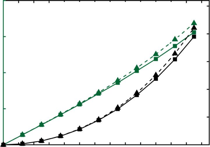
shown in Fig. 1a, and this TA is generally actuated by where V is the applied voltage, R is the electrical resistance,
Joule heating. The modeled PS and Ta TAs have two leg and ρ is the electrical resistivity. The subscripts Ta and PS
pairs with a leg length L = 150 μm and an offset O = denote the Ta and PS actuators, respectively. The (L/A)
5 μm, as defined in Fig. 1a. This same leg geometry is terms cancel. Measured data give ρTa = 20 µΩ cm and
studied throughout this work. ρPS = 2000 µΩ cm.
a
+ -
I
I
Actuation
Leg offset, O = 5 μm
Leg length, L = 150 μm
b 60 c
600 600
Thermal actuator voltage (V)
10 PTa/PPS ≈ 1:2.5 es
s
50 tr
VTa/VPS ≈ 1:16 ag
e 500 legs 500
Temp. change (°C)
8 lt ax
vo r 40 m
we
Stress (MPa)
PS Ta 400
Power (mW)
po 400 ss
6 PS re
30 st 300
r 300 leg
4 owe 20 ax
Ta p m
SΔ
T 200
PS P
10 200
2 100
Ta voltage
0 100 ΔT 0
0 Ta
ΔTTa/ΔTPS ≈ 1:2
0 –100
0 0.5 1 1.5 2 2.5 3 3.5 4 0 0.5 1 1.5 2 2.5 3 3.5 4
Maximum displacement (μm) Maximum displacement (μm)
Fig. 1 Modeled comparison of Ta between polysilicon (PS) thermal actuators. a Schematic of V-shaped thermal actuators. Dimensions indicated
are assumed throughout this article, b comparison of actuation voltages and powers, and c maximum temperature and stress for PS and Ta actuators
at different maximum displacements, as predicted by the electro-thermo-mechanical model. The circles indicate operating points discussed in
subsection “Model”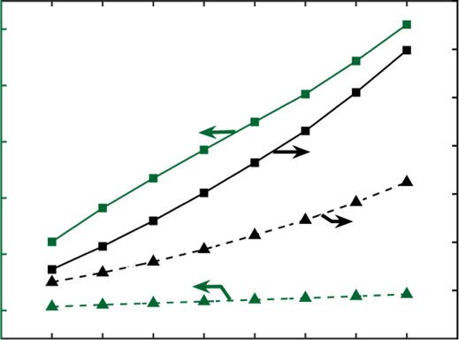
Ni et al. Microsystems & Nanoengineering (2021)7:6                                                                        Page 4 of 13

   For a small gap between the legs and the substrate, the               we choose t = 2.5 μm to guarantee in-plane motion for an
major source of heat loss in a gaseous atmosphere is                     aspect ratio of 2.5:1. Then, σ op
                                                                                                         c  1:6 ´ σ c .
                                                                                                                      ip

thermal conduction from the legs to the substrate and                       The actuation voltage and current to achieve a targeted
depends only weakly on the TA material. Hence, we further                displacement of the shuttle are more accurately predicted
approximate that for the same power, the increase in                     using the coupled model than with the zeroth-order model.
actuator leg temperature, ΔT, is the same. However, αTa ≈                The property values used are listed in Supplementary Table
6 µε/°C, while αPS ≈ 3 µε/°C. Therefore, for the same power              S1. The Ta-to-PS actuation voltage ratio is found to be 1:16
delivered, the Ta TA deflects twice as much as the PS TA.                 in comparison with 1:14. This is mainly because the real CTE
If the Ta TA power P is halved, its deflection is the same as             ratio, αTa:αPS, is more than 2:1 (αTa = 6.3 µε/°C25 and αPS =
that of the PS TA. Hence, we take PTa/PPS = 0.5. With this               2.5 µε/°C13 at room temperature). The actuation voltage ratio
consideration, Eq. (1) is rearranged, and values are inserted:           is found to be independent of displacement. The 16× lower
                                                                         voltage of Ta TAs than of PS TAs means that these actuators
                          sffiffiffiffiffiffiffiffiffiffiffiffiffiffiffiffiffiffiffiffiffiffiffiffiffiffiffiffiffiffi
              ffiffiffiffiffiffiffiffiffiffiffiffiffiffiffiffiffiffiffiffiffiffiffiffiffiffiffi
             s                                                      can operate at 0.3 V for a measured displacement of 1.5 μm,
    VTa           PTa          ρTa           0:5  20          1
        ¼                                 ¼                   :         as shown in subsection ‘Thermal actuator characterization’,
    VPS           PPS          ρPS            1  2000         14
                                                                         which makes them compatible with CMOS (≤1.8 V). Addi-
                                                                   ð2Þ   tionally, the power consumption is decreased by 60%, in
                                                                         comparison with the zeroth-order model decrease of 50%.
  Therefore, to zeroth-order, for the same deflection, a Ta               These results are shown in Fig. 1b, where the actuation
TA operates at half the power and a 14 times lower vol-                  voltages and power consumptions of PS and Ta TAs at
tage than the PS TA. As PS actuators typically operate at                different maximum displacements are presented, and the
5–10 V, Ta TAs operate at 0.5–1 V.                                       predicted data previously discussed are circled.
  A coupled MATLAB/ANSYS simulation is used to                              The temperature change due to Joule heating is not
model the thermal conduction paths in detail13. We use                   uniform along the TA legs. While the anchors are at room
bulk Ta material properties from the refs. 25–27 for                     temperature, the maximum temperature generally occurs
modeling. This model has been validated for PS, and we                   at a location between the anchors and the shuttle. A high
use it to refine the zeroth-order estimates.                              operating temperature can lead to softening, plastic
  In cross-section, the leg thickness t is 2.5 μm, while the             deformation, or creep of the structural material. In air,
width w is 1 μm. These choices are important and are                     oxidation can affect the maximum temperature, as dis-
explained as follows:                                                    cussed in subsection “Thermal actuator characterization”.
                                                                         Therefore, a smaller increase in temperature while
   (i) A beam width of 1 μm is readily within our optical
                                                                         maintaining the desired displacement/force output is
       lithography capabilities. This ensures a well-
                                                                         important for achieving reliable TAs. Due to its higher
       controlled output force, which is highly sensitive
                                                                         CTE, Ta actuators experience less than half of the max-
       to the change in beam width13.
                                                                         imum temperature change compared to PS. For a mea-
  (ii) The critical out-of-plane buckling stress, σ op
                                                    c , must             sured displacement of 1.5 μm, Ta TAs operate at a
       be higher than the critical in-plane buckling stress,
                                                                         temperature change of ~75 °C. This is much lower than
       σ ip
         c to ensure the desired in-plane motion. We                     Tm/3, above which creep is generally assumed to initiate
       evaluate the worst-case scenario, i.e., a beam offset
                                                                         for metals. The maximum temperature change along the
       angle θ = 0, for two beams that are mirrored and
                                                                         actuator legs is presented in Fig. 1c (olive lines), and the
       connected at the shuttle. For unconstrained
                                                                         predicted data previously discussed are circled.
       actuation, a sufficient condition is t > w. However,
                                                                            Stress is another factor that can plastically deform the
       the ratio t:w must increase further if the in-plane
                                                                         structural material or accelerate creep at elevated tem-
       motion of TA is constrained. For example, during
                                                                         peratures. The predicted maximum operating stress near
       nanomechanical tensile testing, TAs are used to
                                                                         the anchors is also plotted in Fig. 1c (black lines). Because
       apply a load, and their in-plane motion is
                                                                         of a slightly higher Young’s modulus, Ta TAs have a
       constrained by the specimen. For constrained in-
                                                                         higher operating stress than PS. If the displacement is
       plane motion, the effective length of the legs
                                                                         larger than 3 μm, the stress exceeds the yield strength of
       doubles, and then
                                                                         bulk Ta (~250 MPa)28. This issue is addressed in sub-
                                                                     section “Preliminary experiments to assess whether Ta
    σ op     π 2 Et 2 = 3 ´ ð2LÞ2     t 2
      c
                              2 ¼      :                        ð3Þ   can be integrated into MEMS”.
    σ ip
      c      π 2 Ew2 = 3 ´ ðLÞ       2w
                                                                         Self-actuation
  Hence, the film thickness t must be at least twice the                    Self-actuation is achieved by raising the ambient tem-
beam width w to deter out-of-plane buckling. Therefore,                  perature, leading to a uniform temperature in the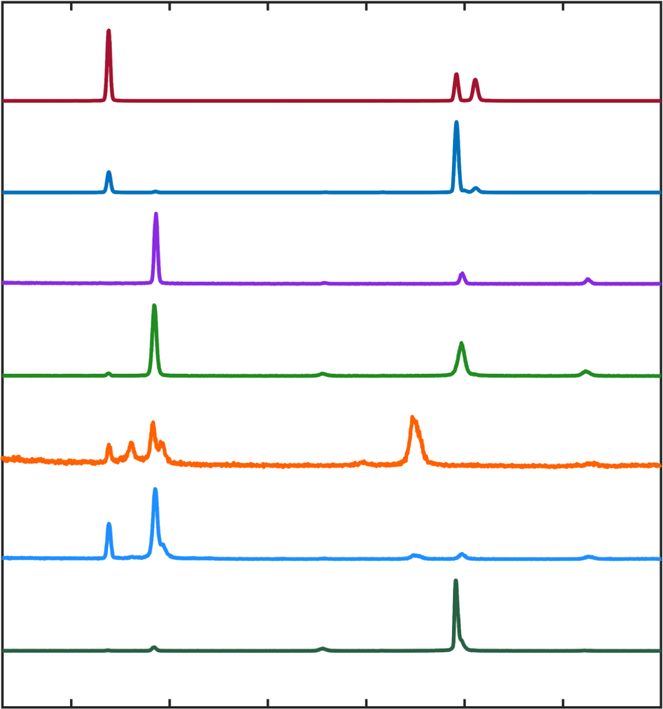
Ni et al. Microsystems & Nanoengineering (2021)7:6                                                              Page 5 of 13

actuator legs. An FEA model is developed using ANSYS               thin film Ta is generally nanocrystalline. Is it strong
to predict the displacement of the shuttle as the tem-             enough to survive the bending stress, as predicted
perature changes. Only one actuator leg pair is con-               in Fig. 1c?
sidered, as the displacement does not depend on the             C. PS is typically annealed at 1000 °C to reduce
number of legs. Boundary conditions include fixed con-              stress17. Is it possible to control the Ta film
straints at two ends of the leg pair (anchors) and a tem-          residual stress while eliminating subsequent
perature change. An example model result of a deformed             annealing steps or minimizing their temperatures?
leg pair subjected to a temperature change, ΔT = 100 °C,        D. Does the Ta thin film possess comparable CTE to
is shown in Supplementary Fig. S1.                                 bulk Ta?
  The displacement of the shuttle, δ, due to a homo-            E. The film thickness is 2.5 μm to prevent out-of-
geneous temperature change, ΔT, can also be obtained               plane buckling. However, if α-Ta is chosen, the
analytically, as follows29                                         thickest α-Ta feature patterned by conventional
                                                                   reactive ion etching (RIE) with good sidewall
                        sinðθÞ                                     protection reported in the literature is only
    δ ¼ αΔTL                            ;           ð4Þ
                 sin ðθÞ þ cos2 ðθÞ AL
                    2               12I
                                       2
                                                                   100 nm31. Is it possible to etch a much thicker
                                                                   α-Ta film and achieve a vertical sidewall for slender
where α is the effective CTE, and I = tw3/12 is the                (1 μm wide) TA legs?
moment of inertia of the actuator leg cross-section.
                                                               This section describes experiments that examine these
                                                             issues.
Model summary
  The more detailed models support our expectation from      Phase selection
the zeroth-order model that Ta has important advantages        When deposited directly onto thermally grown oxide,
over PS as a TA structural material because Ta exhibits      Ta assumes the tetragonal β-phase, as indicated by a
the following:                                               relatively high resistivity of ρ = 173 µΩ cm. This high
                                                             ρ phase (170–210 µΩ cm) is of interest in thin film
    (i) a 16× lower driving voltage, compatible              resistors and heaters and is a potential material for
        with CMOSs,                                          magnetoresistive random access memory technologies. As
   (ii) a 60% lower electric power consumption,              the sputter pressure decreases, energetic particle bom-
  (iii) a 50% lower operating temperature for the same       bardment is intensified and results in a higher compres-
        displacement, and                                    sive residual stress32. For repeatable operation, a lack of
  (iv) the capability of self-actuation.                     intrinsic (or growth) stress change is needed at the
                                                             potential operating temperatures. However, the com-
  In the next section, we assess whether Ta is a viable      pressive stress in β-Ta is fully relaxed, and a tensile biaxial
structural material for surface micromachining.              residual stress, σ bR , of 400–600 MPa results after a 700 °C
                                                             annealing step. This annealing step is performed in an
                                                             argon-purged rapid thermal anneal (RTA) chamber at
Preliminary experiments to assess whether Ta can be          atmospheric pressure. To minimize oxidation, the Ta is
integrated into MEMS                                         covered by plasma-enhanced chemical vapor deposition
  A thorough investigation of whether Ta can be inte-        (PECVD) SiO2 that is 1 μm thick, which is stripped by RIE
grated into a conventional MEMS fabrication process flow      after annealing. Figure 2 presents the σ bR values of blanket
as a structural material has not previously been reported.   β-Ta films deposited from 3.3 to 4.8 mTorr before and
Additionally, the electrothermomechanical model uses         after annealing.
the bulk Ta material properties listed in Supplementary        The σ bR change results from a β-to-α phase transfor-
Table S1. It remains unclear whether Ta thin films possess    mation. The X-ray diffraction (XRD) diagram in Fig. 3a
comparable properties. To demonstrate Ta as a viable         confirms that the as-deposited films are the pure tetra-
structural material, the following questions must be         gonal β-phase. Upon 20 min of annealing at 500 °C, β-Ta
explicitly answered:                                         partially transforms to α-Ta, as presented in Fig. 3b.
                                                             When the temperature is increased to 700 °C, the β-to-α
   A. Unlike bulk Ta, which assumes the equilibrium bcc
                                                             phase transformation is complete within 10 min, as shown
      α-phase, thin film Ta deposits more readily in the
                                                             in Fig. 3c. This phase transformation causes the film to
      metastable tetragonal β-phase30. Which of these is
                                                             contract due to the differences in β- and α-phase densities
      the better candidate?
                                                             and due to significant grain growth30. As the contraction
   B. Bulk Ta has a low yield strength (~250 MPa)28, but
                                                             is constrained, high tension results30,33.
Ni et al. Microsystems & Nanoengineering (2021)7:6 Page 6 of 13
vacuum is broken, a mixture of α- and β-phases with ρ =
600 After 700 °C anneal 30.0 µΩ cm is obtained, with the most intense peak from
Biaxial residual stress (MPa)
400
α-Ta (Fig. 3f). It is likely that sputter cleaning removes
most chromium oxide, but residue remains. Therefore,
200 successive Cr/Ta depositions or a sufficiently long sputter-
Tension
0 cleaning step is needed to avoid the formation of β-Ta.
Compression
–200 Hardness enhancement
–400
Before anneal We find that the strength of α-Ta films is significantly
enhanced over that of bulk Ta. The nanoindentation
3.2 3.4 3.6 3.8 4.0 4.2 4.4 4.6 4.8
hardness, H, is 7.47 ± 0.46 GPa at RT. This corresponds to a
Sputter pressure (mTorr)
yield strength σy ≈ H/3 = 2.5 GPa, which is ten times greater
Fig. 2 β-Ta films exhibit a high tensile stress after anneal. Residual than bulk Ta. Therefore, even at a deflection of 4 µm, the
stress of β-Ta films as a function of sputter pressure before and after
maximum bending stress of ~600 MPa, as shown in Fig. 1c,
annealing at 700 °C
remains well below σy with a safety factor of ~4. A Young’s
modulus of 188 ± 6 GPa is also measured at RT, comparable
(002) to that of bulk Ta, with a value of 185 GPa34. We also
(721)
(513) a measure the hardness and Young’s modulus of α-Ta films
(110) ex situ after annealing at atmospheric pressure from
b 400–1000 °C in an argon-purged RTA chamber. These
(110) properties are stable even after annealing at 1000 °C. H
(200) (112) (220) c measurements, along with the bulk Ta data at room tem-
(110) (112) perature (RT) from the literature34, are shown in Fig. 4a.
Intensity (a. u.)
d
(410) (202) This strength enhancement arises from the fine-grained
(212) (522)
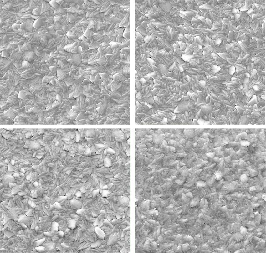
e microstructure. Top views of Ta films in the as-deposited
condition and after annealing are shown in Fig. 4b–e.
(002) (110)
f According to the Hall-Petch relationship, nanocrystalline Ta
(112) should have a higher σy than bulk Ta, which can have a grain
(110) (200) g size on the order of several hundred micrometers. Guisbiers
et al.35 obtained a Hall-Petch coefficient of 58 GPa nm1/2 by
30 40 50 60 70 80 90 measuring the hardness of Ta films with different grain sizes.
2 θ (deg.) Based on this strengthening coefficient, our measured
Fig. 3 Phase and preferential orientation changes of Ta films hardness of 7.47 GPa for the as-deposited films corresponds
under different deposition and annealing conditions. XRD to an average grain size of ~160 nm, which is in reasonable
diagrams of a as-deposited β-Ta films, b β-Ta films after annealing at agreement with Fig. 4b. Although no obvious change in grain
500°C for 20min reveals nucleation of α-Ta films, c β-Ta films after size is observed after annealing at 600 °C and 800 °C (Fig. 4c,
annealing at 700°C for 10min, d as-deposited α-Ta films on a Cr seed
layer, vacuum NOT broken, e as-deposited α-Ta films on a Cr seed
d), voids are formed after annealing at 1000 °C (Fig. 4e).
layer, vacuum broken, NO sputter clean, f as-deposited α-Ta films on a The lack of noticeable grain growth may be rationalized
Cr seed layer, sputter clean, and g α-Ta after hydrogen degas by the low homologous temperature (i.e., at T = 800 °C,
(described in subsection “Full fabrication sequence”) T/Tm = 0.33), the relatively short 30 min annealing time,
and the inferred grain size of 160 nm. In comparison,
Chookajorn et al.36 annealed pure W with a 20-nm grain
To avoid the phase transformation, the more stable bcc size at T/Tm = 0.37 for 1 week, and grains grew to
α-Ta phase is preferred. This phase exhibits a low ρ of ~600 nm. The larger initial grain size in Ta and the
15–60 µΩ cm, making it an attractive choice for lower shorter annealing time indicate that the lack of grain
power TAs. The α-phase can grow on a 10-nm-thick growth inferred here is not unreasonable. Additionally, an
Cr seed layer. Its bcc unit cell structure is confirmed by the increased electrical resistivity of 22.5 µΩ cm and 27.0 µΩ
XRD diagram in Fig. 3d, and ρ is measured as 21.4 µΩ cm. cm (compared to 21.4 µΩ cm) is measured after annealing
However, we find that a freshly prepared seed layer is at 800 °C and 1000 °C, respectively. Since Ta resistivity
essential to grow α-Ta. If the vacuum is broken between increases with oxygen content37, trace oxygen may be
the Cr and Ta depositions, then Ta grows in the pure incorporated into the film during the annealing steps,
β-phase (Fig. 3e). This is likely due to the immediate oxi- leading to pinning of grain boundaries38. Peak broadening
dation of Cr when it is exposed to air. By sputter cleaning could not be detected in the X-ray analysis due to the
the substrate with a bias voltage of −40 V for 45 s after the relatively large grain size. However, the annealing steps do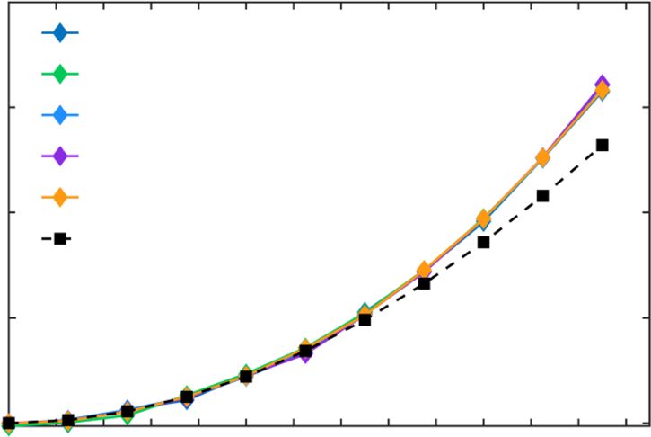
Ni et al. Microsystems & Nanoengineering (2021)7:6 Page 7 of 13
biaxial residual stress σ bR of sputter-deposited α-Ta can be
a
12 Bulk Ta 200 well controlled during deposition by adjusting the sputter
pressure. A compressive σ bR is observed at lower sputter
nc-Ta film
Young’s modulus (GPa)
10 pressures due to enhanced energetic particle bombard-
150
ment32. This value increases linearly with pressure and
Hardness (GPa)
8
nc-Ta film becomes tensile at a critical sputter pressure of ≈
6 100 4.8 mTorr. The σ bR versus sputter pressure slope is shal-
lower than the steep stress change for Ta around the
4
50 critical sputter pressure reported by Thornton et al.40.
2 Bulk Ta This makes it easier to achieve near-zero stress, allowing
for a greater process margin. The σ bR versus sputter
0
As-deposited 400 600 800 1000
0
pressure data of α-Ta are presented in Supplementary
Anneal temperature (°C) Fig. S3.
b As-deposited
c 600 °C Coefficient of thermal expansion
The CTE is a key property needed to predict TA
behavior. The stress changes in blanket α-Ta films as a
function of temperature during heating and cooling cycles
in air are shown in Supplementary Fig. S4. For cubic
materials, CTE is isotropic. In each cycle, the film deforms
thermoelastically, and the slopes are constant and nearly
500 nm 500 nm
identical from RT to 150 °C. The curve fitting results
using the least-squares method are shown in Supple-
d 800 °C
e 1000 °C mentary Fig. S4. Based on Eq. (5) (see Materials and
Methods), the average Δα of the heating and cooling
Void stages is 3.2 ε/°C. Using an αSi of 2.7 µε/°C15, αTa is
determined to be 5.9 µε/°C. This is in good agreement
with the published bulk Ta CTE of 6.3 µε/°C25. The
material properties of bulk Ta, Ta thin films, and PS at
room temperature are summarized in Table S2.
500 nm 500 nm
Reactive ion etching
Fig. 4 Strength of thin film α-Ta remains stable after anneals up
to 1000 °C. a ɑ—Hardness and modulus of α-Ta films in the as- A major challenge arising from the large aspect ratio of
deposited condition and after annealing at 400–1000°C (solid) and 2.5:1 of the TA legs is vertical etching of the sidewalls.
hardness of bulk Ta at room temperature (dashed). α-Ta films of 2.5 µm This large thickness-to-width ratio may be associated with
thickness with grain size of about 160 nm in the b as-deposited severe lateral etching. This leads to a loss of shape and leg
condition and after 30min annealing at c 600°C, d 800°C, and e 1000 °C
width, which can significantly change the output force of
TAs13. It is known that α-Ta is more difficult to pattern
using RIE than β-Ta30,41. Much work has established that
result in a change in the preferential orientation. Com- due to the high volatility of Ta fluoride and chloride, Ta
pared with the XRD diagram of the as-deposited films can be etched by conventional plasma etching based on
(Fig. 3d), the (112) orientation becomes increasingly fluorine42–44, chlorine45, or interhalogen compounds44.
dominant as the annealing temperature increases, as However, these studies were mostly carried out for β-Ta
shown in Fig. S2. The films remain in the α-phase, and no or unpatterned α-Ta films. To the best of our knowledge,
new phase is formed. A more detailed microstructural the thickest reported α-Ta feature patterned by conven-
study after annealing is an important topic for future tional RIE with good sidewall protection is 100 nm31. This
work. Additionally, it is known that fatigue causes grain was achieved using a SiCl4–NF3 gas mixture that is not
growth in nanocrystalline metals39, but the grain size of typically available in a standard cleanroom environment.
Ta TAs undergoing thousands of actuation cycles is not Thicker α-Ta structures of 350–400 nm were also etched,
evaluated in this work. but they were patterned by an unconventional electron
cyclotron resonance ion stream with a mixture of chlorine
Residual stress control and fluorine gases46.
As mentioned above, postdeposition annealing is Using fluorine-based RIE, we perform work with an
usually needed to reduce PS residual stress. However, the extensive scope to improve sidewall protection for the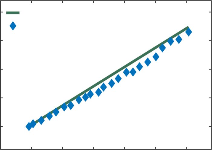
Ni et al. Microsystems & Nanoengineering (2021)7:6                                                                       Page 8 of 13

                                                                        mask. Because the hard mask is thin, a positive photo-
                                                                        resist with only a 400 nm thickness can be used to max-
                                                                        imize the resolution. The Cr hard mask is ion milled, as
                                                                        assisted by end-point detection to avoid any redeposition
                                                                        effect, and the photoresist is stripped by a gentle oxygen
                                                                        plasma application (Fig. 6a). Next, the Ta film is subjected
                                                                        to RIE using CF4 and Ar (Fig. 6b). The etch rate is
                                                                        ~42 nm/min. Subsequently, the Cr hard mask is stripped
                  –Ta                                                  selectively by a Cr wet etchant, followed by the removal of
                                                                        the sacrificial thermal oxide at room temperature by BHF
                  SiO2                                                  (5 parts 40% NH4F:1 part 49% HF) for 1 h. Critical point
                                                                        drying (CPD) results in the freestanding structures
                   Si                                                   (Fig. 6c).
                                                     5 μm
                                                                          At a constant sputter pressure, the stress gradient is
 Fig. 5 A high thickness-to-width ratio of 2.5:1 is achieved with       85 MPa/μm (Fig. 6d), which causes unacceptable curvature
 minimal lateral etch. α-Ta RIE showing vertical sidewalls. Remaining   in the shuttle, as it contacts the substrate, as shown in
 islands in the field areas are swept away upon release                  Supplementary Fig. S5. Therefore, during the Ta deposition
                                                                        step, the sputter pressure is varied to balance the intrinsic
                                                                        stress gradient. Supplementary Table S3 shows a protocol
1 μm feature. We find that O2, which is often added to                   in which the sputter pressure is gradually decreased. The
etch chemicals to release more fluorine and to boost the                 stress gradient can be determined from the tip deflection of
etching rate42,43,45, can substantially enhance lateral                 cantilever beams, δ, using the following equation47:
etching. In contrast, the addition of Ar improves aniso-
tropy. We also find that α-Ta exhibits a significant mac-                     dσ uR     E 2
                                                                                  ¼          δ;                                  ð6Þ
roloading effect: sidewall protection is generally much                      dz     1  ν l2
better for a wafer than for a chip. Other process para-
meters, including pressure, gas flow and power, are                      where l is the beam length, σ uR is the uniaxial residual
also found to influence the extent of the lateral etching.               stress, and z is the out-of-plane direction. The tip
Our efforts resulted in minimal lateral etching and a                   deflection is measured by interferometry. The cantilever
vertical sidewall profile after a 1 h RIE step (Fig. 5) under            beam bends up, meaning that the stress shifts toward
the optimal conditions.                                                 tension as the film deposition continues. The results for
                                                                        “sputter pressure varied during deposition” are presented
Full fabrication sequence                                               in Fig. 6d. By utilizing decreasing sputter pressures, the
  The evidence from subsection “Preliminary experiments                 stress gradient decreases to 30 MPa/μm, and the tip
to assess whether Ta can be integrated into MEMS”                       deflection is almost three times smaller. As sputter
indicates that thin film α-Ta possesses the properties                   pressures both higher and lower than the critical sputter
required for a promising TA material and, importantly,                  pressure are used, the average σ bR of the as-deposited
that it can be processed by conventional MEMS fabrica-                  blanket Ta film remains at a low level of approximately
tion methods. Therefore, in this section, we evaluate a full            −40 MPa. With this sequence, the released TA shuttle
fabrication sequence for Ta TAs. Outstanding issues are                 becomes freestanding. The stress gradient is measured
as follows:                                                             after a hydrogen degas annealing step, as explained next.
                                                                          After the BHF release step, we observe that the residual
    1. Although the legs in TAs are fixed on both sides,
                                                                        stress shifts substantially toward compression. The resi-
       the shuttle itself will bend if the residual stress
                                                                        dual stress changes increase linearly with BHF exposure
       gradient is too high. Can the stress gradient be
                                                                        time and reach −1 GPa after 150 min. This is because
       sufficiently well controlled?
                                                                        during the release step, BHF injects atomic hydrogen into
    2. Ta is reported to survive a buffered hydrofluoric
                                                                        the film, which expands the crystal structure and results
       acid (BHF) release etching step. However,
                                                                        in compressive stress, as reported in the literature48. To
       hydrogen can readily diffuse into metal films and
                                                                        remove hydrogen and recover the as-deposited residual
       change the residual stress. Does this occur, and can
                                                                        stress, we degassed the sample at 500 °C under ultrahigh
       it be reversed?
                                                                        vacuum (UHV). This annealing step leads to a change in
  The proposed full fabrication process flow is shown in                 the preferential orientation of the film (Fig. 3g), similar to
Fig. 6a–c. Following deposition of a 2.5-μm-thick α-Ta                  the data in Fig. S2. After degassing the sample, the stress,
film, a 45-nm-thick Cr layer is deposited as an etch hard                extracted using fixed-fixed beams, is largely recovered but
Ni et al. Microsystems & Nanoengineering (2021)7:6                                                                                                              Page 9 of 13

                                                                                                                        e
    Cr hard mask                                                                                                                     Actuator displaces
                                                                                                                                       during release
              Ta, 2.5 μm
              SiO2, 1 μm                               7
    a              Si                                  6       d
                                                       5

                                     Deflection (μm)
                                                                               Constant sputter pressure
                                                       4                       85 MPa/μm
        Ta                   Ta                                                                                                                           Shuttle hops
                                                       3                                                                                                  over adjacent
                   SiO2
                                                                                                                                                          pad
    b              Si                                  2
                                                       1
                                                       0                   Sputter pressure varied during deposition
        Ta                                                                 30 MPa/μm
                                                           0       25     50     75    100    125   150     175   200
    c            Si                                                              Location (μm)
                                                                                                                                       ≈ 12 μm

                                                                                                                            100 μm

 Fig. 6 α-Ta films are integrated into a full MEMS fabrication process but issues of large stress gradient and hydrogen incorporation arise.
 Fabrication process: a 2.5-μm-thick α-Ta is deposited on the substrate, followed by deposition of a 45-nm-thick Cr hard mask which is patterned by
 photolithography and ion mill, b Ta is RIE’d using fluorine-based chemicals, and c the Cr seed layer and hard mask and the sacrificial oxide are
 stripped, structures are rendered freestanding by CPD and degassed at 500°C in UHV to remove injected hydrogen in the release step,
 d deflections of 193-μm-long cantilever beams, and e a 12-µm displacement of a TA after BHF release due to hydrogen injection, corresponding to
 1.24 GPa compressive stress

                                                                                                           Thermal actuator characterization
                                                                                                           As-released structure
                                  Shuttle                                                                     Enormous and unexpected in-plane TA displacements
                                                                                                           of ~12 µm are initially observed after release (Fig. 6e).
                Current
                                                                                                           This corresponds to a residual compressive stress of
                                                                                                           1.24 GPa, and this problem lead us to discover the
                                                                                                           hydrogen injection phenomenon discussed above and
                                                                                                           solve it using the postrelease UHV annealing step48. With
                                                                        Leg
                                                                                                           this annealing step, the in-plane displacement after release
        Vernier                                                         pairs
         scale
                                                                                                           is ~5 µm, corresponding to a stress of −340 MPa. The TA
                                                                                                           is fabricated using a blanket Ta film with a uniaxial stress
                                                                                                           of approximately −27 MPa. Therefore, the stress change
                                                                                                           after the UHV annealing step is approximately −310 MPa,
        100 μm
                                                                                                           which is higher than that measured in fixed-fixed beams
                                                                                                           (−60 MPa)48. The reason for this result is likely that TA
 Fig. 7 Functional α-Ta TAs are fabricated after stress gradient                                           legs are much narrower (1 µm wide) than fixed-fixed
 reduction and hydrogen degas. Top view of freestanding Ta                                                 beams (10 or 20 μm wide) and have a higher surface-to-
 thermal actuator. In-plane deflection δ ≈ 5µm after hydrogen
 degas step
                                                                                                           volume ratio. This makes them absorb more hydrogen
                                                                                                           than the wide fixed-fixed beams, meaning that more
                                                                                                           hydrogen may remain in the film after the UHV step. We
                                                                                                           deem this adequate for TA characterization, but in future
is still 50–60 MPa more compressive than the initial                                                       work, a final stress near zero is, in principle, achievable by
stress. More details about stress recovery can be found in                                                 further adjustments of the sputter pressure or by a longer
the literature48.                                                                                          degassing period. We will present other approaches that
  Following the process flow in Fig. 6a–c, α-Ta TAs are                                                     resolve this problem in a future publication.
successfully fabricated. The TA shown in Fig. 7 has 16 leg                                                    Figure 5 shows that the Ta RIE leaves residue between
pairs, with the same leg geometry as in Fig. 1. TA legs with                                               the lines. We find that these small islands are swept away
this geometry are used for characterization, as discussed                                                  during the release process, and therefore, the appearance
next.                                                                                                      of the chips is clean, as seen in Fig. 7.
Ni et al. Microsystems & Nanoengineering (2021)7:6 Page 10 of 13
a b 0.4
2 10
1st cycle Measurement (dashed)
Change in displacement (μm)
Thermal actuator voltage (V)
2nd cycle
1.5 0.3 8
3rd cycle
Power (mW)
4th cycle
6
5th cycle
1 0.2
Simulation
4
0.5 Simulation
0.1 (solid)
2
0 0 0
0 1 2 3 4 5 6 7 8 9 10 11 12 13 0 1 2 3 4 5 6 7 8 9 10 11 12 13
Current per leg (mA) Current per leg (mA)
c d
2 Analytical
150
Measurements
Actual temperature (°C)
Displacement (μm)
120 y = 0.5818x + 9.325 1.5
90 1
60 0.5
30
0
0
0 30 60 90 120 150 180 210 240 270 0 25 50 75 100 125 150
Temperature setpoint (°C) Temperature (°C)
Fig. 8 Characterization of α-Ta TAs by Joule heating and self-actuation is in good agreement with simulations. a Displacement as a function
of current per leg for five actuation cycles, b modeled and measured actuation voltage and electric power consumption as a function of current per
leg, c temperature calibration. The abscissa is the hotplate temperature setpoint and the ordinate is the TA actual temperature and d self-actuation
displacement as a function of temperature
Actuation by Joule heating diamond markers), along with the model results (dashed
All displacements reported below are in-plane and are line, square markers). Repeatable actuation for five
with respect to the displacement after release. The dis- actuation cycles is demonstrated. The measurements show
placements are measured as a function of current in air agreement with the model up to 6.3 mA/leg, but dis-
and compared to the electrothermomechanical model placement is enhanced at higher current levels. We attri-
results. A Vernier scale is imaged under a 50× objective bute this result to a higher actual leg temperature than the
lens during actuation and is used to determine the dis- modeled temperature, as explained next. The model con-
placement of the shuttle by pattern matching, which has a siders widely spaced leg pairs and assumes that they are
resolution of ~5 nm. Ta is susceptible to internal oxida- thermally isolated from each other, as is valid when the
tion49, and we observe oxidation at 100 °C without pro- separation is ~100 μm or more13. However, in our design,
tection. The measurements reported are performed with the heated leg pairs are spaced by only 10 μm. This leads to
TAs protected by a 20-nm-thick Al2O3 passivation layer less efficient heat dissipation and an overall higher leg
deposited by atomic layer deposition (ALD), which temperature for a given current. The effect becomes
increases the oxidation-resistant temperature to ~150 °C. increasingly important as heat generation increases at
While further improved passivation is a topic for future higher currents. This is verified by our observation that
research, under high vacuum conditions that can be TAs with the same geometry but with a leg spacing of only
achieved in test chambers50 or in electron microscopes, 5 μm in fact generate even greater displacement at the
the operating temperature is likely to be substantially same current due to this self-heating effect.
higher (minimal oxidation up to 750 °C is reported in the Additionally, the actuation voltage and electric power
literature51). consumption are measured as a function of current per leg.
The displacement of a TA as a function of current per They are also predicted by the electrothermomechanical
leg for five actuation cycles is plotted in Fig. 8a (solid line, model, as described in subsection “Model”, using theNi et al. Microsystems & Nanoengineering (2021)7:6 Page 11 of 13
measured Ta thin film properties. The as-fabricated TAs and process temperatures. The demonstration is based on
have 16 leg pairs, but only two leg pairs are modeled, so the systematic studies of material properties, including
measured power consumption is divided by 8 to normalize Young’s modulus, hardness, and CTE; key fabrication
this difference. These results are plotted in Fig. 8b. An challenges, including phase changes, anisotropic etching,
overall agreement between the measurements and the residual stress control, hydrogen incorporation, and des-
model is evident. The measured actuation voltage and orption; and modeling and measurements of two different
power are slightly higher at high currents due to the self- actuation mechanisms, i.e., conventional actuation by
heating effect, as previously explained, which slightly Joule heating and self-actuation. The following conclu-
increases the electrical resistivity. The low power con- sions are supported by the evidence provided:
sumption and actuation voltage (below 0.35 V) of Ta TAs ●
The Ta to polysilicon actuation voltage ratio is
are confirmed by these measurements.
approximately 1:16, making Ta TAs compatible with
The repeatable results indicate that Ta oxidation is a
CMOS. The electric power consumption of Ta TAs
minor issue up to the estimated maximum leg temperature
is decreased by 60% for the same displacement
(including self-heating) of 120 °C. Including the residual
(Fig. 1b).
stress inferred from the 0 V displacement, our model cal- ●
Ta TAs can operate at half the maximum
culates that the maximum operating stress in the legs is
temperature change of polysilicon for the same
approximately +500 MPa (tension) and −610 MPa (com-
displacement. Although the leg bending stress is
pression). Similarly, the strength of nanocrystalline Ta is
slightly higher, Ta TAs retain a high safety factor
well above the operating stress.
(Fig. 1c).
●
A β-to-α phase transformation leads to full
Self-actuation
relaxation of the compressive stress and a tensile
Self-actuation is tested in air on a hot plate using optical
stress of 400–600 MPa. It is preferred to deposit Ta
microscopy, and displacements are again measured using a
in the bcc α-phase by introducing a Cr seed layer
Vernier scale. Temperature calibration is necessary because
(Figs. 2 and 3).
heat transfer is imperfect. Therefore, we measure the ●
α-Ta films have a significantly larger hardness value
resistivity of actuator legs in situ using the four-point probe
of 7.47 ± 0.46 GPa at RT than bulk Ta. This
configuration. By knowing the temperature coefficient of
corresponds to a ≈10× higher yield strength. The
resistance (TCR) of Ta, +3800 p.p.m./°C52, the actual
hardness and Young’s modulus remain stable even
temperature of the TA legs, Tact, is deduced after waiting
after annealing up to 1000 °C (Fig. 4a).
15 min to establish a steady-state condition at each setpoint ●
The average biaxial residual stress of α-Ta films can
temperature, Tsp. Above the reference temperature at RT,
be well controlled by adjusting the sputter pressure,
Tact is ~60% of Tsp, revealing the critical importance of
which is characterized by a gradual stress change
calibration. The Tact values are plotted in Fig. 8c.
near the critical sputter pressure (Supplementary
An effective CTE of Δα = 3.2 µε/°C, i.e., the difference
Fig. S3).
between the CTEs of Ta and the Si substrate, is used for ●
The CTE of α-Ta films is ~5.9 ε/°C, comparable to
the models. The FEM model results are essentially iden-
that of bulk Ta (Supplementary Fig. S4).
tical to the analytical model results. For the measure- ●
A vertical sidewall profile and minimal lateral
ments, the temperature is stepped up in increments of
etching are achievable for the TA legs (Fig. 5).
10 °C. Over the range from RT to 150 °C, the agreement ●
By varying the sputter pressure in situ, the stress
with the model is good. The measured self-actuation in-
gradient is reduced from 85 MPa/μm to 30 MPa/μm
plane displacement as a function of Tact and that of the
(Fig. 6d).
analytical model are shown in Fig. 8d. ●
Following conventional surface micromachining
For this specific TA design, the temperature sensitivity
(Fig. 6a–c), α-Ta TAs are successfully fabricated
is ~14 nm/°C. This can be adjusted by changing the TA
(Fig. 7).
leg geometry and can be further improved by certain ●
Repeatable actuation by Joule heating is
amplification designs, such as cascaded structures12, for
demonstrated. Overall, the measured displacement
different applications. In addition, a comprehensive
agrees with the modeling but deviates at a high
comparison of V-shaped TAs made of Ta, PS, Ni, and SU-
current due to limited heat dissipation (Fig. 8a).
8 can be found in Tables S4. A, B. ●
Self-actuation is demonstrated by increasing the
ambient temperature. The measurements agree well
Conclusions
with the modeling and analytical solutions (Fig. 8d).
This work demonstrates the promising application of
Ta as a new structural material for TAs with advantages The maximum TA displacement in air can be increased by
over polysilicon including low voltage and lower operating developing improved passivation layers. While not exploredNi et al. Microsystems & Nanoengineering (2021)7:6 Page 12 of 13
herein, this micromachined structural Ta material can, in and contributed to the process flow. M.P.dB. supervised the research and
principle, also be used to construct many other MEMS revised the manuscript.
devices, including but not limited to fixed-fixed beams48, Conflict of interest
comb drives, resonators, optical components, accel- The authors declare that they have no conflict of interest.
erometers, and gyroscopes. We note that these devices do
not require elevated temperatures to operate. The maximum Supplementary information accompanies this paper at https://doi.org/
10.1038/s41378-020-00232-z.
process temperature is 500 °C. Therefore, Ta is a candidate
structural material for post-CMOS processing53,54. Received: 8 June 2020 Revised: 4 October 2020 Accepted: 19 November
2020
Materials and methods
The substrates used are 4″ (100) Si wafers with a
1-µm-thick thermally grown oxide layer. A load-locked DC
magnetron sputtering system (CVC Connexion Cluster References
Tool) is used to deposit Ta films at a base pressure lower 1. Messner, W. C. et al. A CMOS-MEMS rotary microactuator suitable for hard disk
than 7 × 10⁻⁸ Torr without intentional heating or biasing drive applications. In TRANSDUCERS 2009 - 15th Int. Conf. Solid-State Sensors,
Actuators Microsystems 1509–1512 (IEEE, USA, 2009).
using Ar as the working gas. At a power of 250 W, the 2. Chu, L. L. & Gianchandani, Y. B. A micromachined 2D positioner with elec-
deposition rate is ~19 nm/min. Crystal structures are trothermal actuation and sub-nanometer capacitive sensing. J. Micromech.
determined on blanket films using XRD under conventional Microeng. 13, 279–285 (2003).
3. Chu, J. & Chen, Z. A novel SU-8 electrothermal microgripper based on the
reflective configurations with a copper Kα source operated type synthesis of the kinematic chain method and the stiffness matrix
at 45 kV and 40 mA (Philips X’pert Pro MRD, model no. method. J. Micromech. Microeng. 21, 54030–54045 (2011).
PW3040/60). Resistivity is measured using a standard four- 4. Angelov, T. et al. Thermo-mechanical transduction suitable for high-speed
scanning probe imaging and lithography. Microelectron. Eng. 154, 1–7 (2016).
point probe configuration. The Young’s modulus and 5. Chiou, J. C. & Lin, W. T. Variable optical attenuator using a thermal actuator
hardness are determined by nanoindentation55. array with dual shutters. Opt. Commun. 237, 341–350 (2004).
Based on the Stoney equation56, the biaxial residual stress 6. Lara-Castro, M. et al. Design and modeling of polysilicon electrothermal
actuators for a MEMS mirror with low power consumption. Micromachines 8,
σ R is found by measuring the curvature change in substrates
b
203 (2017).
before and after deposition using the laser scanning method 7. Saqib, M., Saleem, M. M., Mazhar, N., Awan, S. U. & Khan, U. S. Design and
with a Tencor Flexus tool (FLX-2320). The CTE of Ta is analysis of a high-gain and robust multi-DOF electro-thermally actuated
MEMS gyroscope. Micromachines 9, 577 (2018).
determined using the same tool and method by measuring 8. Park, J. S., Chu, L. L., Oliver, A. D. & Gianchandani, Y. B. Bent-beam electro-
the stress change as the temperature varies from RT to thermal actuators-Part II: Linear and rotary microengines. J. Microelectromech.
150 °C. The relationship between the biaxial stress change, Syst. 10, 255–262 (2001).
9. Khazaai, J. J., Haris, M., Qu, H. & Slicker, J. Displacment amplification and
Δσ bR , and the temperature change, ΔT, is as follows: latching mechanism using V-shape actuators in design of electro-thermal
MEMS switches. In Proc. IEEE Sensors 1454–1459 (IEEE, USA, 2010).
E 10. Saleh, M. E., Beuth, J. L., Picard, Y. N. & de Boer, M. P. In situ platform for
Δσ bR ¼ ΔαΔT ; ð5Þ isothermal testing of thin-film mechanical properties using thermal actuators.
1ν J. Microelectromech. Syst. 24, 2008–2018 (2015).
where E and v are the Young’s modulus and Poisson’s ratio 11. Shin, J. et al. Controlling dislocation nucleation-mediated plasticity in nanos-
tructures via surface modification. Acta Mater. 166, 572–586 (2019).
of the films, respectively, and Δα is the difference in CTE 12. Que, L., Park, J. S. & Gianchandani, Y. B. Bent-beam electrothermal actuators-
values between the Ta film and the Si substrate. part I: single beam and cascaded devices. J. Microelectromech. Syst. 10,
The CTE of single crystalline Si is well known. Therefore, 247–254 (2001).
13. Baker, M. S., Plass, R. A., Headley, T. J. & Walraven, J. A. Final Report: Compliant
the CTE of Ta films can be determined by plotting Δσ bR Thermo-Mechanical MEMS Actuators, LDRD #52553. Sandia Report No.
ΔT and finding the slope. Sand2004-6635 (Sandia National Laboratories, USA, 2004).
The optimal conditions for Ta RIE are a CF4 flow of 14. Potekhina, A. & Wang, C. Review of electrothermal actuators and applications.
Actuators 8, 69 (2019).
6 sccm, an Ar flow of 30 sccm, a pressure of 20 mTorr, 15. Okada, Y. & Tokumaru, Y. Precise determination of lattice parameter and
and a power of 44 W. thermal expansion coefficient of silicon between 300 and 1500 K. J. Appl. Phys.
56, 314 (1984).
Acknowledgements 16. Gilgunn, P. J., Liu, J., Sarkar, N. & Fedder, G. K. CMOS-MEMS lateral electro-
This work was partially supported by the US National Science Foundation (NSF) thermal actuators. J. Microelectromech. Syst. 17, 103–114 (2008).
grant number CMMI-1635332. We also acknowledge the Kavcic-Moura 17. Howe, R. T. Surface micromachining for microsensors and microactuators. J.
Endowment Fund for the support. We would like to thank the executive manager, Vac. Sci. Technol. B Microelectron. Process. Phenom. 6, 1809 (1988).
Matthew Moneck, and all the staff members of the CMU Eden Hall Foundation 18. Dellaert, D. & Doutreloigne, J. A thermally-actuated latching MEMS switch
Cleanroom for their guidance and advice on equipment usage and process matrix and driver chip for an automated distribution frame. Mechatronics 40,
development. We also acknowledge the use of the Materials Characterization 287–292 (2016).
Facility at Carnegie Mellon University under grant # MCF-677785. 19. Steiner, H., Keplinger, F., Schalko, J., Hortschitz, W. & Stifter, M. Highly efficient
passive thermal micro-actuator. J. Microelectromech. Syst. 24, 1981–1988
Author contributions (2015).
L.N. performed the modeling, developed the MEMS fabrication process, 20. Zhang, R., Chu, J., Wang, H. & Chen, Z. A multipurpose electrothermal
fabricated thermal actuators, characterized the material properties and thermal microgripper for biological micro-manipulation. Microsyst. Technol. 19, 89–97
actuators, and wrote the manuscript. R.M.P. designed the thermal actuators (2013).Ni et al. Microsystems & Nanoengineering (2021)7:6 Page 13 of 13
21. Lu, H. et al. SU8-based micro neural probe for enhanced chronic in-vivo 38. Guo, J. et al. Oxygen-mediated deformation and grain refinement in Cu-Fe
recording of spike signals from regenerated axons. In Proc. IEEE Sensors 66–69 nanocrystalline alloys. Acta Mater. 166, 281–293 (2019).
(IEEE, South Korea, 2006). 39. Meirom, R. A. et al. Fatigue-induced grain coarsening in nanocrystalline pla-
22. Pustan, M. et al. Reliability design of thermally actuated MEMS switches based tinum films. Acta Mater. 59, 1141–1149 (2011).
on V-shape beams. Microsyst. Technol. 23, 3863–3871 (2017). 40. Thornton, J. A., Tabock, J. & Hoffman, D. W. Internal stresses in metallic films
23. Pustan, M., Birleanu, C., Dudescu, C., Muller, R. & Baracu, A. Integrated thermally deposited by cylindrical magnetron sputtering. Thin Solid Films 64, 111–119
actuated MEMS switch with the signal line for the out-of-plane actuation. In (1979).
Symposium on Design, Test, Integration and Packaging of MEMS/MOEMS, DTIP 41. Nakaishi, M., Yamada, M., Kondo, K., Yamabe, M. & Sugishima, K.
2018 1–4 (Institute of Electrical and Electronics Engineers Inc., 2018). Anomalous etching residues of sputter-deposited Ta upon reactive
24. Mølhave, K. & Hansen, O. Electro-thermally actuated microgrippers with ion etching using chlorine-based plasmas. Jpn. J. Appl. Phys. 31,
integrated force-feedback. J. Micromech. Microeng. 15, 1265–1270 (2005). L1625–L1627 (1992).
25. Touloukian, Y. S., Powell, R. W., Ho, C. Y. & Klemens, P. G. Thermophysical 42. Hsiao, R. & Miller, D. Etching of tantalum in fluorine-containing high density
Properties of Matter: Thermal Expansion of Metallic Elements and Alloys Vol. 12 plasmas. J. Electrochem. Soc. 143, 3266–3270 (1996).
(Thermophysical and Electronic Properties Information Center, Lafayette IN, 43. Martz, J. C., Hess, D. W. & Anderson, W. E. Tantalum etching in fluorocarbon/
1975). oxygen rf glow discharges. J. Appl. Phys. 67, 3609–3617 (1990).
26. Taylor, R. E., Kimbrough, W. D. & Powell, R. W. Thermophysical properties of 44. Kuo, Y. Reactive ion etching of sputter deposited tantalum with CF4, CF3Cl,
tantalum, tungsten, and tantalum-10 wt. per cent tungsten at high tem- and CHF3. Jpn. J. Appl. Phys. 32, 179–185 (1993).
peratures. J. Less-Common Met. 24, 369–382 (1971). 45. Yamada, M. An etching mechanism of ta by chlorine-based plasmas. J. Elec-
27. Touloukian, Y. S., Powell, R. W., Ho, C. Y. & Klemens, P. G. Thermophysical trochem. Soc. 138, 496 (1991).
Properties of Matter: Thermal Conductivity of Metallic Elements and Alloys. Vol. 1 46. Tsuchizawa, T. et al. Electron cyclotron resonance plasma etching of α-Ta for x-
(Thermophysical and Electronic Properties Information Center, Lafayette IN, ray mask absorber using chlorine and fluoride gas mixture. Jpn. J. Appl. Phys.
1970). 39, 6914–6918 (2000).
28. Zhang, M., Yang, B., Chu, J. & Nieh, T. G. Hardness enhancement in nano- 47. Ericson, F., Greek, S., Oderkvist, J. S. & Schweitz, J.-A. High-sensitivity surface
crystalline tantalum thin films. Scr. Mater. 54, 1227–1230 (2006). micromachined structures for internal stress and stress gradient evaluation. J.
29. Zhu, Y., Corigliano, A. & Espinosa, H. D. A thermal actuator for nanoscale in situ Micromech. Microeng. 7, 30–36 (1997).
microscopy testing: design and characterization. J. Micromech. Microeng. 16, 48. Ni, L., Karagoz, B., Gellman, A. J. & de Boer, M. P. Compression and decom-
242–253 (2006). pression of structural tantalum films exposed to buffered hydrofluoric acid. J.
30. Knepper, R., Stevens, B. & Baker, S. P. Effect of oxygen on the thermo- Micromech. Microeng. 30, 055011 (2020).
mechanical behavior of tantalum thin films during the β–α phase transfor- 49. Pawel, R. E., Cathcart, J. V. & Campbell, J. J. Stress generation in tantalum during
mation. J. Appl. Phys. 100, 123508 (2006). oxidation. J. Electrochem. Soc. 110, 551 (1963).
31. Shimada, H. & Maruyama, K. Highly selective etching of tantalum electrode to 50. Soylemez, E., Plass, R. A., Ashurst, W. R. & de Boer, M. P. Probing
thin gate dielectrics using SiCI4-NF3 gas mixture plasma. Jpn. J. Appl. Phys. 43, microelectromechanical systems in an environmentally controlled
1768–1772 (2004). chamber using long working distance interferometry. Rev. Sci. Instrum.
32. Windischmann, H. Intrinsic stress in sputter-deposited thin films. Crit. Rev. Solid 84, 075006 (2013).
State Mater. Sci. 17, 547–596 (1992). 51. Liu, L., Wang, Y. & Gong, H. Annealing effects of tantalum films on Si
33. Clevenger, L. A., Mutscheller, A., Harper, J. M. E., Cabral, C. & Barmak, K. The and SiO2/Si substrates in various vacuums. J. Appl. Phys. 90, 416–420
relationship between deposition conditions, the beta to alpha phase trans- (2001).
formation, and stress relaxation in tantalum thin films. J. Appl. Phys. 72, 52. Schwartz, N., Reed, W. A., Polash, P. & Read, M. H. Temperature coefficient of
4918–4924 (1992). resistance of beta-tantalum films and mixtures with b.c.c.-tantalum. Thin Solid
34. Hodgson, D., Wu, M. & Biermann, R. ASM Handbook, Volume 2, Properties and Films 14, 333–346 (1972).
Selection, Nonferrous Alloys and Special-Purpose Materials (ASM International, 53. Fischer, A. C. et al. Integrating MEMS and ICs. Microsyst. Nanoeng. 1, 15005
1990). (2015).
35. Guisbiers, G., Herth, E., Buchaillot, L. & Pardoen, T. Fracture toughness, hardness, 54. De Boer, M. P., Ni, L. & Pocratsky, R. M. Development of tantalum (Ta) as a
and Young’s modulus of tantalum nanocrystalline films. Appl. Phys. Lett. 97, structural material for surface micromachining. Provisional patent No. 63/
(2010). 046736 (2020).
36. Chookajorn, T., Murdoch, H. A. & Schuh, C. A. Design of stable nanocrystalline 55. Oliver, W. C. & Pharr, G. M. An improved technique for determining hardness
alloys. Science 337, 951–954 (2012). and elastic-modulus using load and displacement sensing indentation
37. Gerstenberg, D. & Calbick, C. J. Effects of nitrogen, methane, and oxygen on experiments. J. Mater. Res. 7, 1564–1583 (1992).
structure and electrical properties of thin tantalum films. J. Appl. Phys. 35, 402 56. Stoney, G. G. The tension of metallic films deposited by electrolysis. Proc. R.
(1964). Soc. A Math. Phys. Eng. Sci. 82, 172–175 (1909).You can also read