Bank of America Merrill Lynch Taiwan, Technology and Beyond Conference - Craig De Young Vice President Investor Relations
←
→
Page content transcription
If your browser does not render page correctly, please read the page content below

Bank of America Merrill Lynch
Taiwan, Technology and Beyond Conference

                                   Craig De Young
                  Vice President Investor Relations

                                       Taipei, Taiwan
                                       March 12, 2013
Forward looking statements                                                                                                            Public
                                                                                                                                      Slide 2

 “Safe Harbor” Statement under the US Private Securities Litigation Reform Act of 1995: the matters discussed in this document
may include forward-looking statements, including statements made about our outlook, including expected research and
development expenditures, expected shipments of tools and productivity of our tools, our business model, and lithography
systems development, including the development of EUV and immersion technology and related system capacity.
These forward looking statements are subject to risks and uncertainties including, but not limited to: economic conditions,
product demand and semiconductor equipment industry capacity, worldwide demand and manufacturing capacity utilization for
semiconductors (the principal product of our customer base), including the impact of general economic conditions on consumer
confidence and demand for our customers’ products, competitive products and pricing, the impact of manufacturing efficiencies
and capacity constraints, the continuing success of technology advances and the related pace of new product development and
customer acceptance of new products, our ability to enforce patents and protect intellectual property rights, the risk of
intellectual property litigation, availability of raw materials and critical manufacturing equipment, trade environment, changes in
exchange rates, available cash, distributable reserves for dividend payments and share repurchases, risks associated with our
co-investment program, including whether the 450mm and EUV research and development programs will be successful and
ASML’s ability to hire additional workers as part of the 450mm and EUV development programs, our ability to successfully
complete acquisitions, including the Cymer transaction or the expected benefits of the Cymer transaction.
The foregoing risk list of factors is not exhaustive. You should consider carefully the foregoing factors and the other risks and
uncertainties that affect the business of ASML described in the risk factors included in ASML's Annual Report on Form 20-F and
other documents filed by ASML from time to time with the SEC. ASML disclaims any obligation to update the forward-looking
statements contained herein.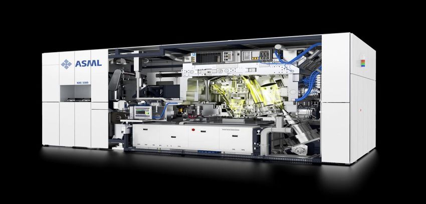
Public
                       Slide 3

Business Environment
Business environment                                                                        Public
                                                                                            Slide 4
                                                                                   17 January 2013

 • We currently plan for 2013 revenues to be at a similar level to
   2012 driven by 28 and 20 nm logic
    •   Slow Q1 start
    •   Recovering in Q2 and a relatively large second half
    •   Expect continued minimum investment level from the memory sector,
        generating an upside revenue opportunity if the PC business picks up
 • 2013 supported by two drivers that are less dependent on
   macroeconomic circumstances:
    •   “Completion” of 28nm capacity installations and “Strategic” technology
        transition to extremely lithography intensive 20nm and below logic nodes
    •   First shipments of 3rd generation EUV tools in preparation for volume
        manufacturing of future generation semiconductors
6 year Sales Review - total net sales M€                                                                               Public

2013 expected at similar level to 2012                                                                                 Slide 5
                                                                                                              17 January 2013

              6000
                                                                         5,651

              5000                                                       1,211   4,732
                                                                4,508
                                                                                 1,023                   Q1
              4000     3,768
                                                                 1,521   1,459                           Q2
  Net Sales

                                                                                                         Q3
                        955          2,954
              3000                                                               1,229                   Q4
                                      494
                        934                                      1,176
                                      697                                1,529
              2000                                1,596                          1,228
                        930           844           581          1,069
              1000
                                                    555                  1,452   1,252
                        949           919                         742
                                                    277
                0                                   183
                       2007          2008          2009          2010    2011    2012    2013 Estimate
                 Numbers have been rounded for readers’ convenience.
Public
                         Slide 6

ASML Business Strategy
Business Model – Focus on “right products on time”                            Public

                                                                              Slide 7

Our business model is derived from our lithography “Value of Ownership”
concept which is based, amongst others, upon the following principles:

• Maintaining an appropriate level of R&D to offer the most advanced
  technologies possible in order to provide the lowest cost for high volume
  production at the earliest possible date enhancing/following Moore’s Law
• Offering ongoing improvements in imaging, overlay and productivity
• Providing high quality customer support, enhancing installed base
  capabilities, improving system reliability and uptimes
• Reducing cycle times between customer order and equipment use in
  production
• Expanding operational flexibility in R&D and manufacturing
Affordable shrink roadmap                                               Public

                                                                              Slide 8
Immersion
            2012   2013    2014   2015    2016    2017   2018   2019   2020

                          NXT:1950i, NXT:1960Bi, NXT:1970Ci
EUV

                                         NXE:3300B, NXE:3350, …
450mm

                                                 QXT, QXE
Significant R&D required to support lithography tool                                                  Public

  development – “the shrink engine”                                                  R&D:               Slide 9
                                                                                               17 October 2012

                                                                 R&D:
                                                                                    ? bln €
                                             R&D:               ~2 bln €
                     R&D:                  ~1.5 bln €
  R&D:             ~400 mln €
~50 mln €

                                                                                     2015s:
                                                                 2010s:           450 mm systems
                                                              NXE EUV systems
                                            2000s:                                     Resolution:
                                                                                  KrF, Immersion, EUV
 1980’s:             1990s:                 Twinscan
                                                                  Resolution:
                                                                   100nm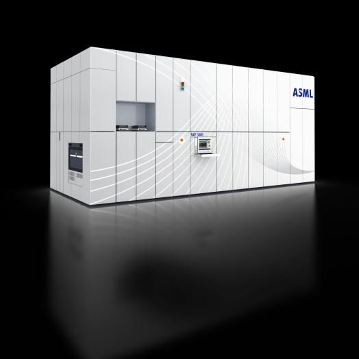
Focus on dual product strategy to match customer
                                                                                      Public

roadmaps                                                                              Slide 10

     TWINSCAN NXT - Immersion                      TWINSCAN NXE - EUV
 •    Continuous improvement in                •   Preparing EUV platform for
      throughput, overlay and imaging              volume manufacturing of critical
      (CDU) optimized for multi-pass               layers with imaging to 10nm
      patterning at 20nm and below                 and beyond
 •    Introduce 450mm capability               •   Introduce 450mm capability

Over 420 ASML immersion systems in use today        6 ASML EUV system in use today
ASML Immersion Product Roadmap Public
NXT:1950i provides performance extendibility until EUV adoption Slide 11
TWINSCAN NXT Extendibility
Upgradeability
2011 Extensions 2012 Extensions 2013+
Matched Machine Overlay 5.5nm 4.5nm 3.5nm
On Product Overlay 9nm 6nm 4nm *
CDU 3nm 1.5nm 1nm
Total focus control budget 110nm 90nm 70nm
Throughput (96 shots) 190 WPH 230 WPH 250 WPH
Defects (ASML test) 10 defects/Wafer 10 defects/WaferASML’s Holistic Lithography Solutions support multi-pass patterning
at 20nm and beyond, will support EUV in future Public
Slide 12
ASML Scanner
Wafer Track
ASML Yieldstar
Yieldstar metrology systems and Litho
InSight software roadmap supports full application
integration to deliver improved On- platform
Product Performance for 20 nm node ( one per fab )
and below
Process window enlargement Process window controlASML Customer Co-Investment Program allows Public
Slide 13
increased R&D investments for key programs
• ASML intends to spend € 750 – 800 million in R&D in 2013
• Co-Investment participants are expected to contribute € 1.4 Billion
in cash for R&D in 2013-2017
• Co-Investment will contribute to:
• Acceleration of EUV development of machines and sources
including next generation EUV systems
• Development of 450 mm litho tools targeting pre-production
systems in 2015/16 and production systems in 2018 (300mm
and 450mm compatible)EUV progress encouraging Public
Slide 14
• Imaging on the production capable NXE:3300B, shows excellent single
imaging results down to 13 nm
• Demonstrated fully integrated EUV source showing extended, stable
exposure power up to 40 Watts, good dose control, full field exposures
• 55 Watts shown in short runs with good key parameter control
• Source design tested successfully at 60 Watts with good debris control
• 11 system ship plan for 2013Eleven NXE:3300B systems in various states of integration in
new clean room completed in 2012 Public
Slide 15
System 1
System 9
Development tool
System 2 New cleanroom
System 6
System 3
System 7
System 4
System 8
System 5 Training 10
ToolNXE technology roadmap has great extendibility Public
Slide 16
first illumination optimization on NA 0.33 system
Under study
Resolution [nm] 32 27 22 16 13 10 7NXE:3300B imaging and overlay beyond expectations Public
Slide 17
Scanner qualification
Filtered S2F Chuck 1 (S2F)
8
Lot (1.3,1.3) X
Dedicated Chuck
Y
6
Overlay [nm]
4
22nm HP 1.3 1.2 1.4
1.0 1.4 1.3
2
BE = 15.9 mJ/cm2
DoF = 160 nm 5 nm
99.7%
x: 1.3 nm
y: 1.3 nm
0
Full wafer CDU = 1.5nm 1 2 3 Day
Filtered S2F (S2F)
Scanner capability 8
Matched Machine Overlay
Lot (3.4,3.0) X
NXE- immersion [nm]
Y
6
3.5 3.2
4 2.7 3.0
2.3 3.3
2
13 nm HP 18 nm HP 23 nm HP 99.7%
x: 3.4 nm
5 nm y: 3.0 nm
XT:1950i reference wafers
0 )
1 2 3 WaferResolution shown on NXE:3300B for dense line spaces, regular
and staggered contact holes; all single exposures Public
Slide 18
14nm HP 14nm HP 18nm HP 19nm HP
13nm HP 13nm HP 17nm HP 18nm HP
Dipole30, Dipole45,
Quasar 30 (CAR) Large Annular (CAR)
Chemically Amplified Resist Inpria Resist
(CAR)EUV Source Power Progress Public
Slide 19
incl. throughput estimates for NXE:3300B EUV system
1000 In die dose
variation
power
EUV(W)Power from the source[W] 250
Estimated productivity
TPT NXE3350 125
80
100 NXE:3300B [Wafers/hr] 126
@15 mJ/cm² 40 81
30 58
33
10
10
5
2
At 40 W: Simulated die yield 99.99% at 0.2%
1 dose, over 6 consecutive runs of > 1 hr
representing > 300 exposed wafers @ 15
mJ/cm2ASML - Cymer merger agreement status Public
Slide 20
17 January 2013
• In Q4 2012, we announced the intended cash-and-stock
acquisition of lithographic light source supplier Cymer
• As part of the regulatory review process, clearance has been
granted by the Committee on Foreign Investment in the United
States (CFIUS), the German and Israeli anti-trust authorities
• Merger agreement approved by Cymer’s shareholders February
2013
• Awaiting regulatory approvals from US, Japan, Taiwan and Korea
• We continue to expect the transaction to close in H1 2013You can also read