ADC DAC Interface v1.0 - LogiCORE IP Product Guide - Xilinx
←
→
Page content transcription
If your browser does not render page correctly, please read the page content below
ADC DAC Interface v1.0

LogiCORE IP Product Guide
Vivado Design Suite

PG388 (v1.0) May 16, 2022

Xilinx is creating an environment where employees, customers, and
partners feel welcome and included. To that end, we’re removing non-
inclusive language from our products and related collateral. We’ve
launched an internal initiative to remove language that could exclude
people or reinforce historical biases, including terms embedded in our
software and IPs. You may still find examples of non-inclusive
language in our older products as we work to make these changes and
align with evolving industry standards. Follow this link for more
information.
Table of Contents
       Chapter 1: Introduction.............................................................................................. 4
          Features........................................................................................................................................ 4
          IP Facts..........................................................................................................................................5

       Chapter 2: Overview......................................................................................................6
          Navigating Content by Design Process.................................................................................... 6
          Core Overview..............................................................................................................................6
          Licensing and Ordering.............................................................................................................. 7

       Chapter 3: Product Specification........................................................................... 8
          Port Descriptions.........................................................................................................................8

       Chapter 4: Core Architecture................................................................................... 9
          RX path..........................................................................................................................................9
          TX Path........................................................................................................................................14
          PHY.............................................................................................................................................. 14

       Chapter 5: Designing with the Core................................................................... 15
          General Design Guidelines.......................................................................................................15
          Clocking...................................................................................................................................... 16
          Resets..........................................................................................................................................24
          Pin and Bank Rules....................................................................................................................24
          Protocol Description................................................................................................................. 24

       Chapter 6: Design Flow Steps.................................................................................28
          Customizing and Generating the Core................................................................................... 28
          Constraining the Core/Subsystem.......................................................................................... 31
          Simulation.................................................................................................................................. 32
          Synthesis and Implementation................................................................................................32

       Chapter 7: Example Design..................................................................................... 33
          Simulating the Example Design.............................................................................................. 34

PG388 (v1.0) May 16, 2022                                                                                                            www.xilinx.com
                                                                                                       Send Feedback
ADC/DAC Interface IP                                                                                                                              2
Project-Based Simulation......................................................................................................... 35

       Appendix A: Upgrading............................................................................................. 41

       Appendix B: Additional Resources and Legal Notices............................. 42
          Xilinx Resources.........................................................................................................................42
          Documentation Navigator and Design Hubs.........................................................................42
          References..................................................................................................................................42
          Revision History......................................................................................................................... 43
          Please Read: Important Legal Notices................................................................................... 43

PG388 (v1.0) May 16, 2022                                                                                                       www.xilinx.com
                                                                                                   Send Feedback
ADC/DAC Interface IP                                                                                                                         3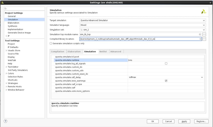
Chapter 1: Introduction

                                                                                       Chapter 1

Introduction
       The ADC/DAC Interface IP is used as high-speed logic for serial to parallel conversion and
       parallel to serial conversion for source synchronous or asynchronous applications. This IP
       involves the calibration for stable sampling of data for RX.

Features
       • Serial to parallel conversion of RX data.
       • Parallel to serial conversion of TX data.
       • Calibration of RX data for maximizing eye opening.
       • IOs can be both single-ended and differential.
       • Serial to parallel ratios of 1:12, 1:14, and 1:16 are supported.
       • All RX lanes are calibrated using a single clock.
       • The number of RX lanes and TX lanes can span across multiple banks. The number of banks in
         the IP is limited to three.

PG388 (v1.0) May 16, 2022                                                                www.xilinx.com
                                                                       Send Feedback
ADC/DAC Interface IP                                                                                  4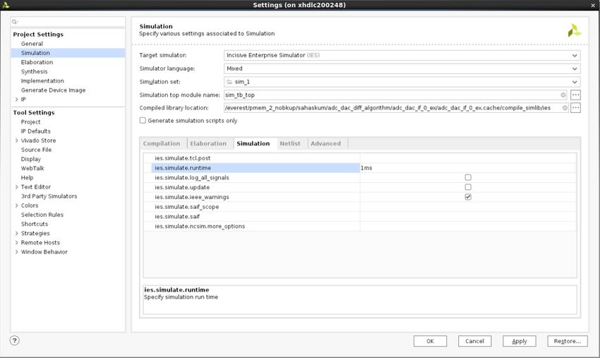
Chapter 1: Introduction

IP Facts
                                                        LogiCORE™ IP Facts Table
                                                        Core or Subsystem Specifics
        Supported Device   Family1                Versal® ACAP
        Supported User Interfaces                 N/A
                                                             Provided with Core
        Design Files                              RTL
        Example Design                            Verilog
        Test Bench                                Verilog
        Constraints File                          XDC
        Simulation Model                          N/A
        Supported S/W Driver                      N/A
                                                            Tested Design Flows2
        Design Entry                              Vivado Design Suite
        Simulation                                For supported simulators, see the Xilinx Design Tools: Release Notes Guide.
        Synthesis                                 Vivado Synthesis
                                                                   Support
        All Vivado IP Change Logs                 Master Vivado IP Change Logs: 72775
                                                            Xilinx Support web page
        Notes:
        1.   For a complete list of supported devices, see the Vivado® IP catalog.
        2.   For the supported versions of third-party tools, see the Xilinx Design Tools: Release Notes Guide.

PG388 (v1.0) May 16, 2022                                                                                         www.xilinx.com
                                                                                        Send Feedback
ADC/DAC Interface IP                                                                                                           5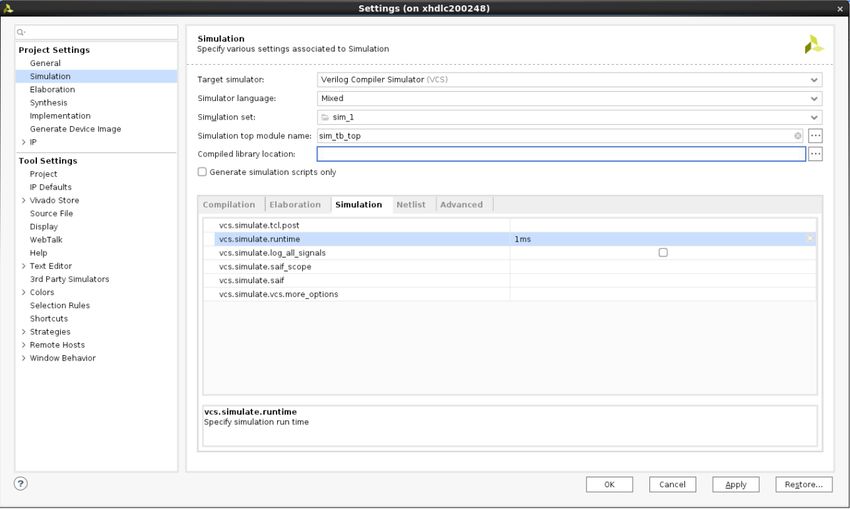
Chapter 2: Overview

                                                                                         Chapter 2

Overview

Navigating Content by Design Process
       Xilinx® documentation is organized around a set of standard design processes to help you find
       relevant content for your current development task. All Versal® ACAP design process Design
       Hubs and the Design Flow Assistant materials can be found on the Xilinx.com website. This
       document covers the following design processes:

       • Hardware, IP, and Platform Development: Creating the PL IP blocks for the hardware
         platform, creating PL kernels, functional simulation, and evaluating the Vivado® timing,
         resource use, and power closure. Also involves developing the hardware platform for system
         integration. Topics in this document that apply to this design process include:

          • Protocol Description
          • Clocking
          • Resets
          • Customizing and Generating the Core

Core Overview
       The ADC DAC Interface IP core provides solutions for interfacing with multiple ADCs or DACs.
       Each I/O bank in Versal® devices contains 54 pins (nine nibbles) that can be used for input and
       output. This IP provides options to configure up to three banks as RX lanes or TX lanes. RX lanes
       aid in serial to parallel conversion and TX lanes aid in parallel to serial conversion. The core is
       organized in high-level blocks as follows:

       • Calibration and Tracking: This logic aids in centering of data for RX lanes. This logic only exists
         for RX and does not exist for TX lanes.

       • Gearbox: Gearbox logic converts the data from 4-bit data words (Single Ended) or 8-bit data
         words (Differential) to 12/14/16-bit data words for RX lanes. Similarly, for TX lanes gearbox
         logic converts the data from 12/14/16-bit data words for TX lanes to 8-bit data words.

PG388 (v1.0) May 16, 2022                                                                   www.xilinx.com
                                                                        Send Feedback
ADC/DAC Interface IP                                                                                     6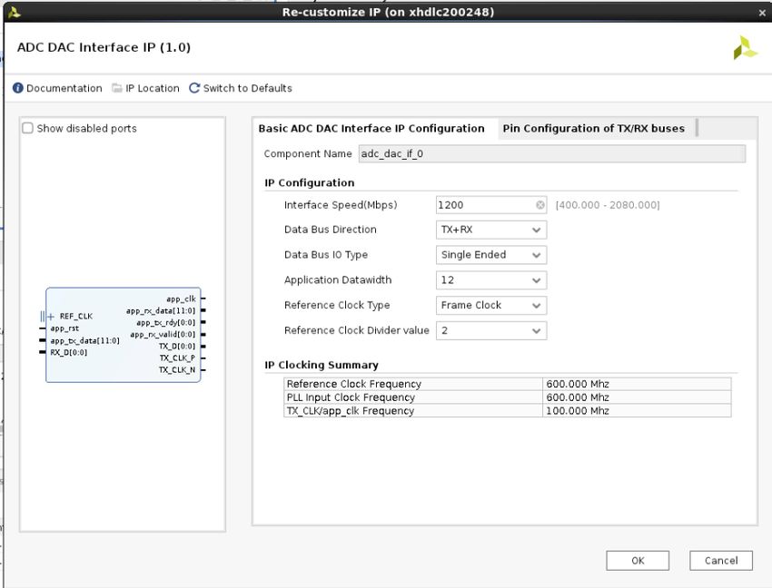
Chapter 2: Overview

       • Physical layer : The physical layer provides a high-speed interface to the ADC and DAC. This
         layer includes the hard blocks inside the Versal ACAP which perform the following:

          • Data serialization and transmission.
          • Data capture and deserialization.
          • High-speed clock generation and synchronization.
          • Coarse and fine delay elements per pin.

                                     Figure 1: ADC DAC Block Diagram

      Versal ACAP
                                                                              REF_CLK_P

                                       Versal ACAP ADC/DAC IF                 REF_CLK_N
                       app_rst
                                               Solution                       TX_CLK_P
                     app_tx_data
                                                                              TX_CLK_N             ADC/
                     app_rx_data
        User                                                                                       DAC
                                                                         TX_D (Single Ended)
       Versal        app_rx_valid                                        TX_{D,N}(Differential)
       ACAP
       Logic                                                             RX_D (Single Ended)
                     app_tx_rdy
                                                                         RX_{D,N}(Differential)

                                                                                                      X25443-061421

Licensing and Ordering
       This Xilinx® LogiCORE™ IP module is provided at no additional cost with the Xilinx Vivado®
       Design Suite under the terms of the Xilinx End User License.

       Information about other Xilinx® LogiCORE™ IP modules is available at the Xilinx Intellectual
       Property page. For information about pricing and availability of other Xilinx LogiCORE IP modules
       and tools, contact your local Xilinx sales representative.

PG388 (v1.0) May 16, 2022                                                                   www.xilinx.com
                                                                     Send Feedback
ADC/DAC Interface IP                                                                                     7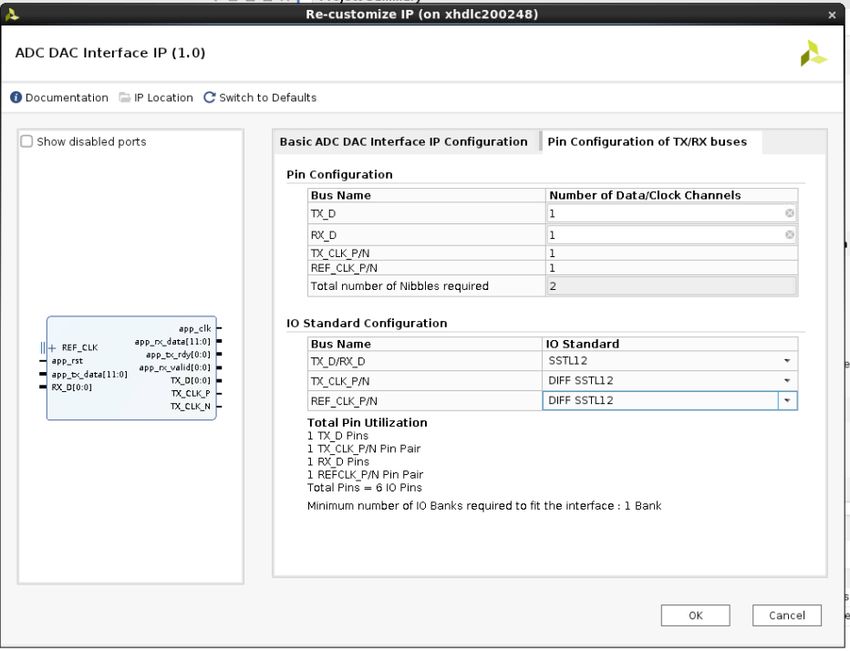
Chapter 3: Product Specification

                                                                                        Chapter 3

Product Specification

Port Descriptions
       There are three port categories at the top-level of the ADC DAC Interface IP core called the
       “user design".

       • The first category is the RX/TX signals that directly interact ADC/DAC. These are described in
         the Protocol Description section.
       • The second category is the application interface signals. These are described in the Protocol
         Description section.
       • The third category includes other signals necessary for proper operation of the core. These
         include the clocks, reset, and status signals from the core. The clocking and reset signals are
         described in their respective sections.

       Related Information

       Protocol Description
       Clocking
       Resets

PG388 (v1.0) May 16, 2022                                                                  www.xilinx.com
                                                                       Send Feedback
ADC/DAC Interface IP                                                                                    8
Chapter 4: Core Architecture
Chapter 4
Core Architecture
This section describes the Xilinx® Versal® adaptive compute acceleration platform (ACAP) ADC
DAC Interface IP core and provides an overview of the modules and interfaces. The core
architecture is shown in the following figure.
Figure 2: Core Architecture
Versal ACAP
Versal ACAP ADC DAC Interface Solution
TX Gearbox logic
ADC/DAC
User Physical
FPGA Logic Layer
RX Gearbox RX Calibration
logic Logic
X25434-060821
RX path
The RX path performs the deserialization of single-bit data on the RX lane to parallel application
data of width 12, 14, or 16. Once deserialization is complete, app_rx_valid is asserted high.
After this, you can sample the data. Deserialization is done in the following steps:
• Deserialization in PHY.
PG388 (v1.0) May 16, 2022 www.xilinx.com
Send Feedback
ADC/DAC Interface IP 9Chapter 4: Core Architecture
• Calibration and tracking of RX data.
• Gearbox logic.
Deserialization in PHY
After internal calibration in the PHY is complete, the PHY converts the single-bit data into 8-bit
parallel data for each RX lane independently. This 8-bit data is then passed to calibration logic.
Calibration and Tracking in RX Path
For stable data sampling, data transition should occur in the centre of the clock. This can be
controlled using delay taps in the PHY. Using these delay taps, you can control the relative
placement of the clock with respect to data. Once internal calibration is complete in the PHY and
the PHY passes the deserialized data, this block starts processing it. This block uses the data
from the PHY to control the delay taps of the PHY. The algorithm for calibration is different for
single-ended IO pins and differential IO pins. This is described in the following sections.
Calibration for Single-Ended IO Based Design
The purpose of the calibration block is to ensure that UI sampling is always at the center for
asynchronous signals. The sampling of UI is performed at the same frequency as the data rate.
For example, if the interface speed is 1250 Mbps then the PLL clock frequency should be 1250
MHz. Thus, you are sampling each UI twice: Once in the center of the UI and once at the edge of
UI. The sample from the center of the UI is valid data and the edge sample is used to keep the
clock in the center of the data by updating the delay line. The block diagram of calibration block
is shown in the following figure.
PG388 (v1.0) May 16, 2022 www.xilinx.com
Send Feedback
ADC/DAC Interface IP 10Chapter 4: Core Architecture
Figure 3: Block Diagram of Calibration Implementation for Single-Ended IO Designs
rx_dq
Phase Detector
rx_data
XPHY Gearbox
DEC
INC
rx_data_valid
CNTVALUEIN CAL_DONE
CNTVALUEOUT
CE Line Tracking
INC POSEDGE/
NEGEDGE
LD
RXTX_SEL
X25435-060821
The samples from the delay line are fed into the phase detector circuit to determine if the delay
line value should be increased or decreased. For each UI, two samples are taken from each
bitslice. Depending on whether the clock is early or late, the delay is incremented or
decremented.
Depending on the phase detector output, delay line values are updated after a certain number of
cycles. Once the respective D samples received from the PHY are in the centre of the UI, the
particular bitslice is considered locked. Once the bitslice is locked, of the eight bits given by PHY,
four bits are given to the RX gearbox. Among the eight bits, four bits are selected depending on
whether the data is N centered or P centered.
Calibration for Differential IO-Based Designs
In the differential case, two lane outputs (both P and N) from the PHY are fed to the calibration
block. The sampling of the UI is done at half the frequency of the data rate. For example, if the
interface speed is 1250 Mbps then the PLL clock frequency should be 625 MHz. Thus, you are
sampling each UI only once on one lane. The same UI is sampled again on another lane. The
block diagram of the calibration block for differential IOs is shown in the following figure.
PG388 (v1.0) May 16, 2022 www.xilinx.com
Send Feedback
ADC/DAC Interface IP 11Chapter 4: Core Architecture
Figure 4: Block Diagram of Calibration Implementation for Differential IO Designs
rx_dq_p
rx_dq_n Phase Detector
rx_data
DEC
INC
XPHY Gearbox
rx_data_valid
CNTVALUEIN_{P,N}
CAL_DONE
CNTVALUEOUT_{P,N}
CE_{P,N} Line Tracking
INC_{P,N}
LD_{P,N}
RXTX_SEL_{P,N}
X25436-060821
For differential IOs, the calibration algorithm is different from single-ended IOs. Here two lanes
are fed into the Alexander bang bang detector as opposed to the single-ended algorithm. For the
Alexander bang bang detector to work, one lane should be edge aligned and other lane should be
center aligned. This is achieved according to the following flow chart.
PG388 (v1.0) May 16, 2022 www.xilinx.com
Send Feedback
ADC/DAC Interface IP 12Chapter 4: Core Architecture
Figure 5: Flow Chart for Centering the ‘N’ Lane
Centering Start
Place ‘P’ lane and ‘N’ lane in stable valid region
Move ‘N’ lane till the left edge is found
Move ‘N’ lane till the right edge is found
From Right edge and Left Edge, Calculate the ‘N’ Center
Move ‘P’ lane to find the left edge of noise for ‘P’ lane
Move ‘P’ lane to find the right edge of noise for ‘P’ lane
From left and right edge of the noise, find the ‘P’ edge
End of Centering
X25437-060821
PG388 (v1.0) May 16, 2022 www.xilinx.com
Send Feedback
ADC/DAC Interface IP 13Chapter 4: Core Architecture
As described in the flow chart, P lane is center-aligned and N lane is edge-aligned. After this,
both the bitslices are considered as locked and both lanes are fed to the Alexander Bang Bang
Detector for VT tracking. Depending on whether the clock is early or late, the delay is
incremented or decrement for both the lanes (P and N) respectively. Once the bitslices are
locked, the 8-bit N channel output is given to the RX gearbox.
Gearbox
The RX Gearbox converts the 4-bit or 8-bit output from the calibration block to application data
of width 12, 14, or 16.
TX Path
The TX path performs the serialization from application data of width 12, 14, or 16 to single-bit
data for each lane. Serialization is performed in two steps.
• TX Gearbox: The TX Gearbox converts the data from application data to 8-bit data.
• Serialization in PHY: The PHY serializes the 8-bit data from gearbox into single-bit data.
PHY
The PHY is considered the low-level physical interface to ADCs or DACs. It contains calibration
logic for ensuring reliable operation of the physical interface itself. The PHY contains the
following features:
• Clock and reset generation logic.
• RX and TX datapaths.
The PHY is included in the complete ADC DAC Interface IP core.
PG388 (v1.0) May 16, 2022 www.xilinx.com
Send Feedback
ADC/DAC Interface IP 14Chapter 5: Designing with the Core
Chapter 5
Designing with the Core
This section includes guidelines and additional information to facilitate designing with the core.
General Design Guidelines
Use the Example Design
Each instance of the ADC DAC Interface IP core core or subsystem created by the Vivado design
tool is delivered with an example design that can be implemented in a device and then simulated.
This design can be used as a starting point for your own design or can be used to sanity-check
your application in the event of difficulty. See the Example Design content for information about
using and customizing the example designs for the core or subsystem.
Registering Signals
To simplify timing and increase system performance in a programmable device design, keep all
inputs and outputs registered between the user application and the core or subsystem. This
means that all inputs and outputs from the user application should come from, or connect to, a
flip-flop. While registering signals might not be possible for all paths, it simplifies timing analysis
and makes it easier for the Xilinx® tools to place and route the design.
Recognize Timing Critical Signals
The constraints provided with the example design identify the critical signals and timing
constraints that should be applied.
Make Only Allowed Modifications
You should not modify the core or subsystem. Any modifications can have adverse effects on
system timing and protocol compliance. Supported user configurations of the core or subsystem
can only be made by selecting the options in the customization IP dialog box when the core or
subsystem is generated.
PG388 (v1.0) May 16, 2022 www.xilinx.com
Send Feedback
ADC/DAC Interface IP 15Chapter 5: Designing with the Core
Clocking
The ADC DAC Interface IP core requires at most two XPLLs per I/O bank used by the ADC DAC
interface and BUFGs. These clocking components are used to create the proper clock
frequencies and phase shifts necessary for the proper operation of the ADC DAC interface.
There are two XPLLs per bank. The number of XPLLS instantiated depends on different
conditions. These are given in the following sections.
Clocking Scheme for Single-Ended IO Based Designs
• For single-ended IO designs, one XPLL per bank is instantiated if that bank has any pins (TX
pins or RX pins or both).
• For two-bank or three-bank designs, bank 1 is considered as the master bank and the other
banks are considered as slave banks.
• This XPLL from the master bank provides the following clocks:
• ○ In a multi-bank scenario, the master bank drives the input clock of slave PLLs.
○ Generatesapp_tx_clk/app_rx_clk to the Versal ACAP logic and other clocks that are
used internally for TX/RX gearbox ,Calibration logic, and PHY .
○ CLKOUTPHY to PHY within the master bank.
• The XPLL from the slave bank will drive the CLKOUTPHY to PHY within that bank.
• The following diagram shows the example clocking for a three-bank design which is based on
single-ended IOs.
PG388 (v1.0) May 16, 2022 www.xilinx.com
Send Feedback
ADC/DAC Interface IP 16Chapter 5: Designing with the Core
Figure 6: Sample Clocking Scheme for Single-Ended Three-Bank Design
Slave PLL-0
(Bank-0)
Tx and Rx XPHY
CLKIN CLKOUTPHY
of Bank-0
Master PLL-0
(Bank-1)
CLKOUT0
Input CLKOUT1 app_tx_clk
CLKIN
Clock
app_rx_clk
CLKOUTPHY Tx and Rx XPHY of Bank-1
Slave PLL-1
(Bank-2)
CLKOUTPHY Tx and Rx XPHY
CLKIN
of Bank-2
Clocking Scheme for Single-Bank Design and
Differential IOs
• For single-bank designs, if the bank has only RX pins, only one PLL will be instantiated for that
bank. This PLL will provide:
○ app_rx_clk to the application and other clocks that are used internally for RX gearbox,
PHY, and calibration.
○ CLKOUTPHY to PHY within the bank.
PG388 (v1.0) May 16, 2022 www.xilinx.com
Send Feedback
ADC/DAC Interface IP 17Chapter 5: Designing with the Core
• For single-bank designs, if the bank has only TX pins, only one PLL will be instantiated for that
bank. This PLL will provide:
○ .
○ app_tx_clk to the application and other clocks which are used internally for TX gearbox
and PHY.
○ CLKOUTPHY to PHY within the bank.
• For single-bank designs, if the bank has both TX and RX pins, two PLLs will be instantiated:
○ One PLL is dedicated for TX pins. This PLL provides:
- app_tx_clk to the application and other clocks which are used internally for TX
gearbox and PHY.
- CLKOUTPHY to TX part of PHY within the bank.
○ Other PLL is dedicated for RX pins. This provides :
- app_rx_clk to the application and other clocks which are used internally for RX
gearbox, PHY, and calibration
- CLKOUTPHY to RX part of PHY within the bank.
The following diagram shows the clocking scheme for a sample single bank design with
differential IOs. This bank has both TX pins and RX pins.
PG388 (v1.0) May 16, 2022 www.xilinx.com
Send Feedback
ADC/DAC Interface IP 18Chapter 5: Designing with the Core
Figure 7: Sample Clocking Scheme for a Single-Bank Design and Differential IOs
Bank-0
Master PLL-0
(Bank-0)
CLKOUT1 app_tx_clk
CLKIN
CLKOUTPHY Tx XPHY of Bank-1
Input Clock
Master PLL-1
(Bank-0)
CLKOUT1 app_rx_clk
CLKIN
CLKOUTPHY Rx XPHY of Bank-1
X25395-060421
Clocking scheme for a two bank design and
Differential IOs
For two-bank designs, one of the banks is considered as the master bank and one as the slave
bank. Bank 1 is the master bank and bank 0 is the slave bank.
• If all the pins in both the banks are RX, Only one PLL will be instantiated for each bank.
○ The PLL in the master bank will provide:
- Input clock for the PLL in the slave bank.
PG388 (v1.0) May 16, 2022 www.xilinx.com
Send Feedback
ADC/DAC Interface IP 19Chapter 5: Designing with the Core
- app_rx_clk to the application and other clocks that are used internally for RX
gearbox, calibration logic, and PHY.
- CLKOUTPHY to PHY within the bank.
○ The PLL in the slave bank will provide:
- CLKOUTPHY to PHY within the bank.
• If all the pins in both banks are TX, only one PLL will be instantiated for each bank.
○ The PLL in the master bank will provide:
- Input clock for the PLL in the slave bank.
- app_tx_clk to the application and other clocks that are used internally for TX gearbox
and PHY.
- CLKOUTPHY to PHY within the bank.
○ The PLL in the slave bank will provide:
- CLKOUTPHY to PHY within the bank.
• If either or both of the banks has both TX and RX pins, the clocking scheme be as follows:
○ The first PLL in the master bank will always provide:
- Input clock for the first PLL in the slave bank.
- CLKOUTPHY to TX part of PHY within the bank.
- app_tx_clk to the application and other clocks that are used for TX gearbox and PHY
○ The second PLL in the master bank will always provide:
- Input clocks for the second PLL in the slave bank.
- app_rx_clk to the application and other clocks that are used for RX gearbox, PHY and
calibration.
- CLKOUTPHY to RX part of PHY within the bank.
○ The first PLL in the slave bank will provide CLKOUTPHY to the TX pins in PHY if TX pins
are present in the slave bank. If TX pins are not present in the slave bank, then the
corresponding PLL will not be instantiated.
○ The second PLL in the slave bank will provide CLKOUTPHY to RX pins in PHY if RX pins
are present in the slave bank. If RX pins are not present in the slave bank, then the
corresponding PLL will not be instantiated.
Clocking Scheme for a Three-bank Design and
Differential IOs
For three-bank designs, the middle bank (bank 1) is always considered as the master bank and
other two are slave banks.
PG388 (v1.0) May 16, 2022 www.xilinx.com
Send Feedback
ADC/DAC Interface IP 20Chapter 5: Designing with the Core
• If all pins in the three banks are RX, only one PLL will be instantiated for each bank.
○ The PLL in the master bank will provide:
- Input clock for the PLL in the slave banks.
- app_rx_clk to the application and other clocks that are used internally for RX
gearbox, PHY, and Calibration.
- CLKOUTPHY to PHY within the bank.
○ The PLL in the slave banks will provide:
- CLKOUTPHY to PHY within the bank.
○ If all pins in the three banks are TX, only one PLL will be instantiated for each bank.
- The PLL in the master bank will provide:
- Input clock for the PLL in the slave banks.
- app_tx_clk to the application and other clocks that are used internally for TX
gearbox and PHY.
- CLKOUTPHY to PHY within the bank.
- The PLL in the slave banks will provide:
- CLKOUTPHY to PHY within the bank.
○ If any or all of the banks have both TX and RX pins, the clocking scheme will be as follows.
- The first PLL in the master bank will always provide:
- Input clock for of the first PLL in the slave banks.
- CLKOUTPHY to TX part of PHY within the bank.
- app_tx_clk to the application and other clocks that are used internally for TX
gearbox and PHY.
- The second PLL in the master bank will always provide:
- Input clock for the second PLL in the slave banks.
- app_rx_clk_ to the application and the other clocks that are used internally for the
RX gearbox, PHY, and calibration.
- CLKOUTPHY to RX part of PHY within the bank.
- The first PLL in the slave bank will provide CLKOUTPHY to TX pins in PHY if TX pins are
present in the slave bank. If TX pins are not present in the slave bank then the
corresponding PLL will not be instantiated.
- The second PLL in the slave bank will provide CLKOUTPHY to RX pins in PHY if RX pins
are present in the slave bank. If RX pins are not present in the slave bank then the
corresponding PLL will not be instantiated.
PG388 (v1.0) May 16, 2022 www.xilinx.com
Send Feedback
ADC/DAC Interface IP 21Chapter 5: Designing with the Core
The following diagram shows the sample clocking structure for a sample three-bank design
where all the banks have both TX and RX pins.
Figure 8: Sample Clocking Scheme for a Three Bank Design with TX and RX Pins
Bank-0
Slave PLL-0
(Bank-0)
CLKOUTPHY Tx XPHY of Bank-0
CLKIN
Slave PLL-1
(Bank-0)
CLKOUTPHY Rx XPHY of Bank-0
CLKIN
Bank-1
Master PLL-0
(Bank-1)
CLKOUT0
CLKIN
CLKOUT1 app_tx_clk
CLKOUTPHY Tx XPHY of Bank-1
Input Clock Master PLL-1
(Bank-1)
CLKOUT0
CLKOUT1 app_rx_clk
CLKIN
CLKOUTPHY Rx XPHY of Bank-1
Bank-2
Slave PLL-2
(Bank-2)
CLKOUTPHY Tx XPHY of Bank-2
CLKIN
Slave PLL-3
(Bank-2)
CLKOUTPHY Rx XPHY of Bank-2
CLKIN
X25396-061421
PG388 (v1.0) May 16, 2022 www.xilinx.com
Send Feedback
ADC/DAC Interface IP 22Chapter 5: Designing with the Core
The following diagram shows the clocking structure for a sample three-bank design. Bank 0 has
only TX pins and Bank 2 has only RX pins. Because bank 0 has only TX pins, only one PLL is
instantiated. Because bank 2 has only RX pins, only one PLL is instantiated. The master bank is
instantiated with two PLLs.
Figure 9: Sample Clocking Scheme for a Three-Bank Design
Bank-0
Slave PLL-0
(Bank-0)
CLKOUTPHY Tx XPHY of Bank-0
CLKIN
Bank-1
Master PLL-0
(Bank-1)
CLKOUT0
CLKIN
CLKOUT1 app_tx_clk
CLKOUTPHY Tx XPHY of Bank-1
Input Clock Master PLL-1
(Bank-1)
CLKOUT0
CLKIN CLKOUT1 app_rx_clk
CLKOUTPHY Rx XPHY of Bank-1
Bank-2
Slave PLL-1
(Bank-2)
CLKOUTPHY Rx XPHY of Bank-2
CLKIN
X25397-061421
PG388 (v1.0) May 16, 2022 www.xilinx.com
Send Feedback
ADC/DAC Interface IP 23Chapter 5: Designing with the Core
Resets
An asynchronous reset (app_rst) input is provided. This is an active-high reset and app_rst
must assert for a minimum pulse width of 5 ns. The app_rst can be an internal or external pin.
Pin and Bank Rules
• Pins are divided into three main sections: Data, Strobe, and System Clock.
• Data: RX_D, TX_D, RX_D_P, RX_D_N, TX_D_P, TX_D_N)
• Strobe: TX_CLK_P, TX_CLK_N
• System_Clock: REF_CLK_P, REF_CLK_N
Should fit in maximum of three banks.
• The app_rst port can be placed beyond the three bank boundary, and only in XP (currently
listed as HP in IO planner) banks.
• REF_CLK_P and REF_CLK_N pins must be placed only on GCIO pin pairs.
• GCIO pins for clock routing need to be properly selected:
○ 1 bank case - The clock should be in the same bank. For example, if the IP is spread across
bank 700, REF_CLK_P/N should always be in 700.
○ 2 bank case - The clock can be in either of the 2 banks. For example, if the IP is spread
across 700 701, REF_CLK_P/N is allowed in either 700 or 701.
○ 3 bank case - The clock should always be in middle bank. For example, if 700, 701, 702 is
used REF_CLK_P/N should always be in 701.
• Bank-Sharing rules:
○ Empty nibbles beyond the extreme ends of the interface can be used by other IP pins.
○ Empty pins within an interface nibble can be used only by routethru pins (pins which do not
go through the XPHY).
• TX and RX pins must not be placed in the same nibble. A nibble can have either TX pins or RX
pins.
Protocol Description
The core contains the following interfaces:
PG388 (v1.0) May 16, 2022 www.xilinx.com
Send Feedback
ADC/DAC Interface IP 24Chapter 5: Designing with the Core
• User Interface
• PHY Interface
User Interface
The user interface signals are connected to a Versal ACAP user design. These are described in
the following table.
Table 1: User Interface Signals
Port Direction Port Name Port Description
Output app_tx_clk TX Frame clock output to application from IP
Output app_rx_clk RX Frame clock output to application from IP
Input app_rst Reset from Application to IP
Output app_rx_data[N*M -1] RX output data to the Application for each lane. Here 'N'
denotes the RX deserialization ratio. N could be 12,14 or 16
as configured by user in the GUI. Here ‘M’ denotes the
Number of RX lanes
Output app_rx_valid[M-1] RX output data valid per lane to the Application. Here ‘M’
denotes the Number of RX lanes. This indicates that
calibration is done for that particular lane and data is valid
for that lane
Input app_tx_data[N*P-1] TX input data from the application for each TX labe. Here 'N'
denotes the TX serialization ratio. Here ‘P’ denotes the
number of TX lanes
Output app_tx_rdy[P-1] Data ready for each TX lane to the Application. This signal
indicates that IP is ready for receiving data from application.
Here ‘P’ denotes the Number of TX lanes
app_tx_clk
This output from the IP to the user is clock generated by the IP for TX data. The frequency of this
clock is the interface speed divided by the application data width. The application data width is
either 12, 14, or 16. This clock is used to sample app_tx_data.
app_rx_clk
This output from the IP to the user is clock generated by the IP for RX data. The frequency of
this clock is the interface speed divided by the application data width. The application data width
is either 12, 14, or 16. This clock is used to sample app_rx_data.
app_rst
This input is an asynchronous and active-high reset. The app_rst signal must assert for a
minimum pulse width of 5 ns.
PG388 (v1.0) May 16, 2022 www.xilinx.com
Send Feedback
ADC/DAC Interface IP 25Chapter 5: Designing with the Core
app_rx_data[N*M -1]
This output denotes the RX output data to the application for each lane. Here 'N' denotes the RX
deserialization ratio. N could be 12,14, or 16 as configured in the GUI. Here ‘M’ denotes the
Number of RX lanes.
app_rx_valid[M-1]
This output denotes the RX output data valid per-lane to the Application. Here ‘M’ denotes the
number of RX lanes. This indicates that calibration is done for that particular lane and that data is
valid for that lane. Once data valid is high, you can start sampling app_rx_data for that lane.
app_tx_data[N*P-1]
This input denotes the TX input data from the application for each TX lane. Here 'N' denotes the
TX serialization ratio. ‘N’ could be 12,14, or 16 as configured in GUI. Here ‘P’ denotes the number
of TX lanes.
app_tx_rdy[P-1]
This output indicates data ready for each TX lane to the application. This signal indicates that the
IP is ready to receive data from the application. Here ‘P’ denotes the Number of TX lanes.
RX Interface
The RX interface signals are externally connected from the ADC to the Versal ACAP. These are
described in the following table.
Table 2: RX Interface Signals
Port Direction Port Name Port Description
Input REF_CLK_P, REF_CLK_N Reference Clock input to XPHY
Input RX_D[M-1:0] RX Data Input to XPHY for Single Ended IO Designs
Input RX_D_P[M-1:0] RX Data input to XPHY for Differential IO Designs (P lane of
Differential)
Input RX_D_N[M-1:0] RX Data input to XPHY for Differential IO Designs (N lane of
Differential)
REF_CLK_P, REF_CLK_N
This differential input provides the REF_CLK to the IP. From this clock all other clocks for
operation of IP are generated.
PG388 (v1.0) May 16, 2022 www.xilinx.com
Send Feedback
ADC/DAC Interface IP 26Chapter 5: Designing with the Core
RX_D[M-1:0]
These inputs provide the RX input data for RX lanes. Here, 'M' denotes the number of RX lanes.
This input is for single-ended IO designs.
RX_D_P[M-1:0],RX_D_N[M-1:0]
This differential input provides the RX Data for differential IO based designs.
TX Interface
The TX interface signals are externally connected to the DAC from the Versal ACAP. These are
described in the following table.
Table 3: TX Interface Signals
Port Direction Port Name Port Description
Output TX_D[M-1:0] TX Data output from XPHY for Single Ended IO Designs
Output TX_D_P[M-1:0] TX Data output from XPHY for Single Ended IO Designs (P
lane of Differential)
Output TX_D_N[M-1:0] TX Data output from XPHY for Single Ended IO Designs (N
lane of Differential)
Output TX_CLK_P, TX_CLK_N TX clock output from XPHY.
TX_D[M-1:0]
This output denotes the serialized data of TX lanes. This output is valid only after
TX_CLK_P ,TX_CLK_N starts toggling. This port exists for single-ended IO-based designs only.
TX_D_P[M-1:0],TX_D_N[M-1:0]
This output denotes the serialized data of TX lanes. This output is valid only after TX_CLK_P,
TX_CLK_N starts toggling. This port exists for differential IO-based designs only.
TX_CLK_P,TX_CLK_N
This differential output denotes the TX CLK generate by XPHY. The frequency of this clock is the
same as app_tx_clk. TX_D or {TX_D_P, TX_D_N} are valid only after {TX_CLK_P,TX_CLK_N}
starts toggling.
PG388 (v1.0) May 16, 2022 www.xilinx.com
Send Feedback
ADC/DAC Interface IP 27Chapter 6: Design Flow Steps
Chapter 6
Design Flow Steps
This section describes customizing and generating the core or subsystem, constraining the core
or subsystem, and the simulation, synthesis, and implementation steps that are specific to this IP
core or subsystem. More detailed information about the standard Vivado® design flows and the
IP integrator can be found in the following Vivado Design Suite user guides:
• Vivado Design Suite User Guide: Designing IP Subsystems using IP Integrator (UG994)
• Vivado Design Suite User Guide: Designing with IP (UG896)
• Vivado Design Suite User Guide: Getting Started (UG910)
• Vivado Design Suite User Guide: Logic Simulation (UG900)
Customizing and Generating the Core
This section includes information about using Xilinx® tools to customize and generate the core or
subsystem in the Vivado® Design Suite.
If you are customizing and generating the core or subsystem in the Vivado IP integrator, see the
Vivado Design Suite User Guide: Designing IP Subsystems using IP Integrator (UG994) for detailed
information. IP integrator might auto-compute certain configuration values when validating or
generating the design. To check whether the values do change, see the description of the
parameter in this chapter. To view the parameter value, run the validate_bd_design
command in the Tcl console.
You can customize the IP for use in your design by specifying values for the various parameters
associated with the IP core or subsystem using the following steps:
1. Select the IP from the IP catalog.
2. Double-click the selected IP or select the Customize IP command from the toolbar or right-
click menu.
For details, see the Vivado Design Suite User Guide: Designing with IP (UG896) and the Vivado
Design Suite User Guide: Getting Started (UG910).
Figures in this chapter are illustrations of the Vivado IDE. The layout depicted here might vary
from the current version.
PG388 (v1.0) May 16, 2022 www.xilinx.com
Send Feedback
ADC/DAC Interface IP 28Chapter 6: Design Flow Steps
ADC DAC IF Basic Configuration Tab
Figure 10: ADC DAC IF Basic Configuration Tab
• Interface Speed: This parameter specifies data rate of TX or RX data lane.
• Data Bus Direction: This parameter can be configured as TX, RX or TX+RX. Select the TX
option if all the pins in the design are TX pins. Select the RX option if all the pins in the design
are RX pins. Select RX+TX if the design has both RX and TX pins.
• Data Bus IO Type: This can be chosen as "Single Ended" or "Differential" based on the IO type
for the pins.
• Application Datawidth: This Datawidth can be configured as 12,14, or 16.
• Reference Clock Type: This can be configured as "Frame clock" or "Bit clock". When this
parameter is chosen as "Bit clock", the reference clock frequency will be same as the interface
speed. When this parameter is chosen as "Frame clock", the reference clock frequency will be
"Bit clock" divided by "Reference clock divider value".
PG388 (v1.0) May 16, 2022 www.xilinx.com
Send Feedback
ADC/DAC Interface IP 29Chapter 6: Design Flow Steps
• IP Clocking Summary: This summary table tabulates the clock frequencies of "Reference
clock", "XPLL Clock" and "app_tx_clk/app_rx_clk".
ADC DAC IF Advanced Configuration Tab
Figure 11: ADC DAC IF Advanced Configuration Tab
• TX_D: This parameter specifies the number of TX lanes.
• RX_D: This parameter specifies the number of RX lanes.
• TX_CLK_P/N: This parameters indicates the number of TX_CLK_P/N outputs from the IP. This
parameter is not programmable. This value will be '1' when the number of TX_D lanes is
greater than '0'.
• REF_CLK_P/N: This parameter indicates the number of REF_CLK_P/N inputs to the IP. This
parameter is not programmable. The value of this parameter is always equal to '1'.
• Total Number of Nibbles required: This parameter displays the minimum number of nibbles
required to accomodate the programmed value of TX pins and RX pins.
PG388 (v1.0) May 16, 2022 www.xilinx.com
Send Feedback
ADC/DAC Interface IP 30Chapter 6: Design Flow Steps
• IO Standard configuration: These tabs provide the option to select the IO standard for TX_D,
RX_D, TX_CLK_P/N, and REF_CLK_P/N.
Output Generation
For details, see the Vivado Design Suite User Guide: Designing with IP (UG896).
Constraining the Core/Subsystem
Required Constraints
This section is not applicable for this IP core or subsystem.
Device, Package, and Speed Grade Selections
This section is not applicable for this IP core or subsystem.
Clock Frequencies
This section is not applicable for this IP core or subsystem.
Clock Management
This section is not applicable for this IP core or subsystem.
Clock Placement
This section is not applicable for this IP core or subsystem.
Banking
This section is not applicable for this IP core or subsystem.
Transceiver Placement
This section is not applicable for this IP core or subsystem.
I/O Standard and Placement
The ADC DAC IP generates the appropriate I/O standards and placement based on the
selections made in the Vivado IDE for the interface type and options.
PG388 (v1.0) May 16, 2022 www.xilinx.com
Send Feedback
ADC/DAC Interface IP 31Chapter 6: Design Flow Steps
Simulation
For comprehensive information about Vivado® simulation components, as well as information
about using supported third-party tools, see the Vivado Design Suite User Guide: Logic Simulation
(UG900).
Synthesis and Implementation
For details about synthesis and implementation, see the Vivado Design Suite User Guide: Designing
with IP (UG896).
PG388 (v1.0) May 16, 2022 www.xilinx.com
Send Feedback
ADC/DAC Interface IP 32Chapter 7: Example Design
Chapter 7
Example Design
This section contains information about the example design provided in the Vivado® Design
Suite. Vivado supports Open IP Example Design flow. To create the example design using this
flow, right-click the IP in the Sources window, as shown in the following figure and select Open
IP Example Design.
Figure 12: Open IP Example Design
This creates a new Vivado project. Upon selecting the menu, a dialog box to enter the directory
information for the new design project opens.
Select a directory, or use the defaults, and click OK. This launches a new Vivado project with all
of the example design files and a copy of the IP.
The following figure shows the example design.
PG388 (v1.0) May 16, 2022 www.xilinx.com
Send Feedback
ADC/DAC Interface IP 33Chapter 7: Example Design
Figure 13: Generated Example Design
Simulating the Example Design
The example design provides a synthesizable test bench to generate a PRBS data pattern to test
TX and RX. In this testbench, for RX, a PRBS pattern will be generated at RX IOs. PRBS
generation at RX IOs is non-synthesizable dummy logic. The same pattern will be checked at the
user interface. For TX, PRBS will be generated at user interface. The same pattern will be
checked at TX IOs. PRBS pattern checking at TX IOs would be non-synthesizable dummy logic. If
there are any mismatches between sending and receiving, the pattern error will be flagged.
Simulation will be run for 100 transactions for each lane for both TX and RX. The example design
can be simulated using one of the methods in the following sections.
PG388 (v1.0) May 16, 2022 www.xilinx.com
Send Feedback
ADC/DAC Interface IP 34Chapter 7: Example Design
Project-Based Simulation
This method can be used to simulate the example design using the Vivado Design Suite (IDE).
The Vivado simulator, Questa Advanced Simulator, IES, and VCS tools are used for ADC DAC IF
IP verification at each software release. The following subsections describe the steps to run a
project-based simulation using each supported simulator tool.
Project-Based Simulation Flow Using Vivado
Simulator
1. In the Open IP Example Design Vivado project, under Flow Navigator, select Simulation
Settings.
2. Select Vivado Simulator as the Target simulator.
3. Under the Simulation tab, set the xsim.simulate.runtime to 1 ms (there are simulation RTL
directives which stop the simulation after a certain period of time, which is less than 1 ms) as
shown in the following figure. The Generate simulation scripts only option generates
simulation scripts only. To run behavioral simulation, Generate Scripts Only option must be
de-selected.
4. Set the Simulation Language to Mixed.
5. Apply the settings and select OK.
PG388 (v1.0) May 16, 2022 www.xilinx.com
Send Feedback
ADC/DAC Interface IP 35Chapter 7: Example Design
6. In the Flow Navigator window, select Run Simulation and Run Behavioral Simulation as
shown:
7. Vivado invokes Vivado simulator and simulations are run in the Vivado simulator tool. For
more information, see the Vivado Design Suite User Guide: Logic Simulation (UG900).
PG388 (v1.0) May 16, 2022 www.xilinx.com
Send Feedback
ADC/DAC Interface IP 36Chapter 7: Example Design
Project Based Simulation Flow Using Questa
Advanced Simulator
1. Open the IP Example Design.
2. Under Flow Navigator, select Simulation Settings.
3. Select Questa Advanced Simulator as the Target simulator .
a. Browse to the compiled libraries location and set the path for the Compiled libraries
location.
b. Under the Simulation tab, set the modelsim.simulate.runtime to 1 ms (there are
simulation RTL directives which stop the simulation after certain period of time, which is
less than 1 ms) as shown in the following figure. The Generate simulation scripts only
option generates simulation scripts only. To run behavioral simulation, the Generate
simulation scripts only option must be de-selected.
4. Apply the settings and select OK.
5. In the Flow Navigator window, select Run Simulation and Run Behavioral Simulation as
shown:
PG388 (v1.0) May 16, 2022 www.xilinx.com
Send Feedback
ADC/DAC Interface IP 37Chapter 7: Example Design
6. Vivado invokes the Questa Advanced Simulator and simulations are run in the Questa
Advanced Simulator tool. For more information, see the Vivado Design Suite User Guide: Logic
Simulation (UG900)
Project Based Simulation Flow Using IES
1. Open the IP Example Design.
2. Under Flow Navigator, select Simulation Settings.
3. Select Incisive Enterprise Simulator (IES) as the Target simulator.
a. Browse to the compiled libraries location and set the path for the Compiled libraries
location.
b. Under the Simulation tab, set the ies.simulate.runtime to 1 ms (there are simulation RTL
directives which stop the simulation after certain period of time, which is less than 1 ms)
as shown in the following figure. The Generate simulation scripts only option generates
simulation scripts only. To run behavioral simulation, Generate simulation scripts only
option must be de-selected.
4. Apply the settings and select OK.
PG388 (v1.0) May 16, 2022 www.xilinx.com
Send Feedback
ADC/DAC Interface IP 38Chapter 7: Example Design
5. In the Flow Navigator window, select Run Simulation and Run Behavioral Simulation as
shown:
6. Vivado invokes IES and simulations are run in the IES tool. For more information, see the
Vivado Design Suite User Guide: Logic Simulation (UG900).
Project Based Simulation Flow Using VCS
1. Open the IP Example Design.
2. Under Flow Navigator, select Simulation Settings.
3. Select Verilog Compiler Simulator (VCS) as the Target simulator.
a. Browse to the compiled libraries location and set the path for the Compiled libraries
location.
PG388 (v1.0) May 16, 2022 www.xilinx.com
Send Feedback
ADC/DAC Interface IP 39Chapter 7: Example Design
b. Under the Simulation tab, set the vcs.simulate.runtime to 1 ms (there are simulation RTL
directives which stop the simulation after certain period of time, which is less than 1 ms)
as shown in the following figure. The Generate simulation scripts only option generates
simulation scripts only. To run behavioral simulation, Generate simulation scripts only
option must be de-selected.
4. Apply the settings and select OK.
5. In the Flow Navigator window, select Run Simulation and Run Behavioral Simulation as
shown:
6. Vivado invokes VCS and simulations are run in the VCS tool. For more information, see the
Vivado Design Suite User Guide: Logic Simulation (UG900).
PG388 (v1.0) May 16, 2022 www.xilinx.com
Send Feedback
ADC/DAC Interface IP 40Appendix A: Upgrading
Appendix A
Upgrading
This appendix is not applicable for the first release of the core or subsystem.
PG388 (v1.0) May 16, 2022 www.xilinx.com
Send Feedback
ADC/DAC Interface IP 41Appendix B: Additional Resources and Legal Notices
Appendix B
Additional Resources and Legal
Notices
Xilinx Resources
For support resources such as Answers, Documentation, Downloads, and Forums, see Xilinx
Support.
Documentation Navigator and Design Hubs
Xilinx® Documentation Navigator (DocNav) provides access to Xilinx documents, videos, and
support resources, which you can filter and search to find information. To open DocNav:
• From the Vivado® IDE, select Help → Documentation and Tutorials.
• On Windows, select Start → All Programs → Xilinx Design Tools → DocNav.
• At the Linux command prompt, enter docnav.
Xilinx Design Hubs provide links to documentation organized by design tasks and other topics,
which you can use to learn key concepts and address frequently asked questions. To access the
Design Hubs:
• In DocNav, click the Design Hubs View tab.
• On the Xilinx website, see the Design Hubs page.
Note: For more information on DocNav, see the Documentation Navigator page on the Xilinx website.
References
These documents provide supplemental material useful with this guide:
PG388 (v1.0) May 16, 2022 www.xilinx.com
Send Feedback
ADC/DAC Interface IP 42Appendix B: Additional Resources and Legal Notices
1. Vivado Design Suite User Guide: Logic Simulation (UG900)
2. Vivado Design Suite User Guide: Designing with IP (UG896)
3. Vivado Design Suite User Guide: Getting Started (UG910)
4. Vivado Design Suite User Guide: Implementation (UG904)
5. Vivado Design Suite User Guide: I/O and Clock Planning (UG899)
Revision History
The following table shows the revision history for this document.
Section Revision Summary
05/16/2022 Version 1.0
General updates Made minor technical updates across the document
07/23/2021 Version 1.0
Initial release. N/A
Please Read: Important Legal Notices
The information disclosed to you hereunder (the "Materials") is provided solely for the selection
and use of Xilinx products. To the maximum extent permitted by applicable law: (1) Materials are
made available "AS IS" and with all faults, Xilinx hereby DISCLAIMS ALL WARRANTIES AND
CONDITIONS, EXPRESS, IMPLIED, OR STATUTORY, INCLUDING BUT NOT LIMITED TO
WARRANTIES OF MERCHANTABILITY, NON-INFRINGEMENT, OR FITNESS FOR ANY
PARTICULAR PURPOSE; and (2) Xilinx shall not be liable (whether in contract or tort, including
negligence, or under any other theory of liability) for any loss or damage of any kind or nature
related to, arising under, or in connection with, the Materials (including your use of the
Materials), including for any direct, indirect, special, incidental, or consequential loss or damage
(including loss of data, profits, goodwill, or any type of loss or damage suffered as a result of any
action brought by a third party) even if such damage or loss was reasonably foreseeable or Xilinx
had been advised of the possibility of the same. Xilinx assumes no obligation to correct any
errors contained in the Materials or to notify you of updates to the Materials or to product
specifications. You may not reproduce, modify, distribute, or publicly display the Materials
without prior written consent. Certain products are subject to the terms and conditions of
Xilinx's limited warranty, please refer to Xilinx's Terms of Sale which can be viewed at https://
PG388 (v1.0) May 16, 2022 www.xilinx.com
Send Feedback
ADC/DAC Interface IP 43Appendix B: Additional Resources and Legal Notices
www.xilinx.com/legal.htm#tos; IP cores may be subject to warranty and support terms contained
in a license issued to you by Xilinx. Xilinx products are not designed or intended to be fail-safe or
for use in any application requiring fail-safe performance; you assume sole risk and liability for
use of Xilinx products in such critical applications, please refer to Xilinx's Terms of Sale which can
be viewed at https://www.xilinx.com/legal.htm#tos.
AUTOMOTIVE APPLICATIONS DISCLAIMER
AUTOMOTIVE PRODUCTS (IDENTIFIED AS "XA" IN THE PART NUMBER) ARE NOT
WARRANTED FOR USE IN THE DEPLOYMENT OF AIRBAGS OR FOR USE IN APPLICATIONS
THAT AFFECT CONTROL OF A VEHICLE ("SAFETY APPLICATION") UNLESS THERE IS A
SAFETY CONCEPT OR REDUNDANCY FEATURE CONSISTENT WITH THE ISO 26262
AUTOMOTIVE SAFETY STANDARD ("SAFETY DESIGN"). CUSTOMER SHALL, PRIOR TO USING
OR DISTRIBUTING ANY SYSTEMS THAT INCORPORATE PRODUCTS, THOROUGHLY TEST
SUCH SYSTEMS FOR SAFETY PURPOSES. USE OF PRODUCTS IN A SAFETY APPLICATION
WITHOUT A SAFETY DESIGN IS FULLY AT THE RISK OF CUSTOMER, SUBJECT ONLY TO
APPLICABLE LAWS AND REGULATIONS GOVERNING LIMITATIONS ON PRODUCT
LIABILITY.
Copyright
© Copyright 2021-2022 Xilinx, Inc. Xilinx, the Xilinx logo, Alveo, Artix, Kintex, Kria, Spartan,
Versal, Vitis, Virtex, Vivado, Zynq, and other designated brands included herein are trademarks of
Xilinx in the United States and other countries. All other trademarks are the property of their
respective owners.
PG388 (v1.0) May 16, 2022 www.xilinx.com
Send Feedback
ADC/DAC Interface IP 44You can also read