The Design Process for Google's Training Chips: TPUv2 and TPUv3
←
→
Page content transcription
If your browser does not render page correctly, please read the page content below
This article has been accepted for publication in a future issue of this journal, but has not been fully edited. Content may change prior to final publication. Citation information: DOI 10.1109/MM.2021.3058217, IEEE Micro

                   The Design Process for Google’s Training
                         Chips: TPUv2 and TPUv3
                            Thomas Norrie, Nishant Patil, Doe Hyun Yoon, George Kurian, Sheng Li, James Laudon,
                                              Cliff Young, Norman Jouppi, and David Patterson

              Five years ago, few would have predicted that a software company like Google would build its own
              chips. Nevertheless, Google has been deploying chips for machine learning (ML) training since 2017,
              powering key Google services. These Tensor Processing Units (TPUs) are composed of chips,
              systems, and software, all co-designed in-house. This paper details the circumstances that led to this
              outcome, the challenges and opportunities observed, the approach taken for the chips, a quick review
              of performance, and finally a retrospective on the results. A companion paper describes the
              supercomputers built from these chips, the compiler, and its performance in detail [Jou20].

              Forces Pushing Towards Custom ML Hardware
              In 2013, only one year after AlexNet swept the ImageNet competition [Kri12], Google leaders predicted
              ML would soon be ready to attack difficult problems like production versions of image and speech
              recognition. Alas, these ML models were so computationally expensive that a sustainable service was
              nearly impossible, as Internet service costs scale by the number of users who grow as the service
              improves. The motivation to slash ML inference serving costs led to the TPUv1 inference system,
              deployed successfully in 2015 [Jou17].

              TPUv1 exposed the next bottleneck: ML training. The team quickly pivoted into building the TPUv2
              training system. Two years later, TPUv2 powered key Google services with fast and cost-effective
              training.

              Challenges and Opportunities of Building ML Hardware
              ML training brings challenges relative to ML inference:

                     ●      More computation. More means both the types of computation—for example, backpropagation
                            requires matrix transposition and loss functions—and the amount of computation. An inference
                            calculation typically executes on the order of 109 floating point operations, but Google’s
                            production training applications require 1019–1022 ; more than 10 orders of magnitude larger!
                     ●      More memory. During training, temporary data is kept longer for use during backpropagation.
                            With inference, there is no backpropagation, so data is more ephemeral.
                     ●      Wider operands. Inference can tolerate int8 numerics relatively easily, but training is more
                            sensitive to dynamic range due to the accumulation of small gradients during weight update.
                     ●      More programmability. Much of training is experimentation, meaning unstable workload targets
                            such as new model architectures or optimizers. The operating mode for handling a long tail of
                            training workloads can be quite different from a heavily optimized inference system.
                     ●      Harder parallelization. For inference, one chip can hit most latency targets. Beyond that, chips
                            can be scaled out for greater throughput. In contrast, exaflops-scale training runs need to
                            produce a single, consistent set of parameters across the full system, which is easily
                            bottlenecked by off-chip communication.

              These problems felt daunting initially, plus we had constraints on time and staffing. Time matters
              because each day saved during development accelerates our production training pipeline a day. And as
              for staffing: while Google is teeming with engineers, they’re not all available for our project. Ultimately,
              the TPU team had only a cup from Google’s large engineering pool. Thus, we had to be ambitious to
              overcome the complexities of training, but the time and staffing budget set constraints.

                                                                                                                                                                                                           1

    0272-1732 (c) 2021 IEEE. Personal use is permitted, but republication/redistribution requires IEEE permission. See http://www.ieee.org/publications_standards/publications/rights/index.html for more information.
                        Authorized licensed use limited to: New York University. Downloaded on February 28,2021 at 19:35:57 UTC from IEEE Xplore. Restrictions apply.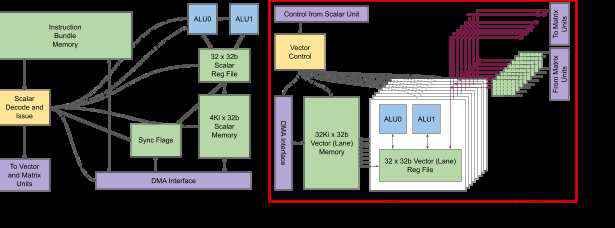
This article has been accepted for publication in a future issue of this journal, but has not been fully edited. Content may change prior to final publication. Citation information: DOI 10.1109/MM.2021.3058217, IEEE Micro
To prioritize, we sorted activities into two buckets: those where we must do a great job, and those that
we only have to do good enough. The first bucket included:
① Build quickly;
② Achieve high chip performance;
③ Scale efficiently to numerous chips;
④ Work for new workloads out of the box; and
⑤ Be cost effective.
Everything else was in the second bucket. While tempting to brush these second bucket issues aside
as minor embarrassments, the reality is building and delivering a good system is as much about what
you decide not to do as what you decide to do. In retrospect, these decisions are not embarrassing
after all!
We refer to the relevant goals using the circled numbers (e.g., ②) throughout the discussion to highlight
“first bucket” design decisions.
Our Approach to ML Hardware
TPUv1 provided a familiar starting point for our training chip (Figure 1a). The high-bandwidth loop (red)
identifies the important part of TPUv1: the core data and computation loop that crunches neural
network layers quickly. DDR3 DRAM feeds the loop at much lower bandwidth with model parameters.
The PCIe connection to the host CPU exchanges model inputs and outputs at even lower bandwidth.
Figure 1 shows five piecewise edits that turn TPUv1 into a training chip. First, splitting on-chip SRAM
makes sense when buffering data between sequential fixed-function units, but that’s bad for training as
on-chip memory requires more flexibility. The first edit merges these into a single vector memory
(Figure 1b and 1c). For the activation pipeline, we moved away from the fixed-function datapath
(containing pooling units or hard-coded activation functions) and built a more programmable vector unit
(Figure 1d) ④. The matrix multiply unit (MXU) attaches to the vector unit as co-processor (Figure 1e).
Loading the read-only parameters into the MXU for inference doesn’t work for training. Training writes
those parameters, and it needs significant buffer space for temporary per-step variables. Hence, DDR3
moves behind Vector Memory so that the pair form a memory hierarchy (also in Figure 1e). Adopting
in-package HBM DRAM instead of DDR3 upgrades bandwidth twentyfold, critical to utilizing the core
②.
Last is scale. These humongous computations are much bigger than any one chip. We connect the
memory system to a custom interconnect fabric (ICI for InterChip Interconnect) for multi-chip training
(Figure 1f) ③. And with that final edit, we have a training chip!
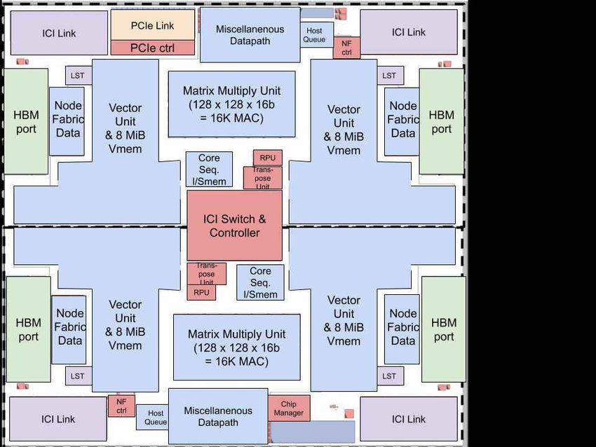
Figure 2 provides a cleaner diagram, showing the two-core configuration. The TPUv2 core datapath is
blue, HBM is green, host connectivity is purple, and the interconnect router and links are yellow. The
TPUv2 Core contains the building blocks of linear algebra: scalar, vector, and matrix computation.
Why two cores? The simpler answer is that we could fit a second core into a reasonably sized chip
②⑤. But then why not build a single, bigger core? Wire latencies grow as the core gets bigger, and the
two-core configuration hits the right balance between reasonable pipeline latency and additional
per-chip computation capacity. We stopped at two bigger cores because they are easier to program as
they allow the developer to reason about one unified instruction stream operating on big chunks of data
④, rather than exposing lots of tiny cores that need to be lashed together. We took advantage of
training fundamentally being a big-data problem.
The following sections dive deeper into key chip components.
2
0272-1732 (c) 2021 IEEE. Personal use is permitted, but republication/redistribution requires IEEE permission. See http://www.ieee.org/publications_standards/publications/rights/index.html for more information.
Authorized licensed use limited to: New York University. Downloaded on February 28,2021 at 19:35:57 UTC from IEEE Xplore. Restrictions apply.This article has been accepted for publication in a future issue of this journal, but has not been fully edited. Content may change prior to final publication. Citation information: DOI 10.1109/MM.2021.3058217, IEEE Micro
Figure 1. Transforming the TPUv1 datapath into the TPUv2 datapath.
Figure 2. TPUv2 datapath in more detail, showing both cores, which appear as a single PCIe
device.
3
0272-1732 (c) 2021 IEEE. Personal use is permitted, but republication/redistribution requires IEEE permission. See http://www.ieee.org/publications_standards/publications/rights/index.html for more information.
Authorized licensed use limited to: New York University. Downloaded on February 28,2021 at 19:35:57 UTC from IEEE Xplore. Restrictions apply.This article has been accepted for publication in a future issue of this journal, but has not been fully edited. Content may change prior to final publication. Citation information: DOI 10.1109/MM.2021.3058217, IEEE Micro
TPUv2 Core
The TPUv2 Core was co-designed closely with the compiler team to ensure programmability ④. (The
compiler’s name is XLA, for accelerated linear algebra [Jou20].) In these discussions, we landed on two
important themes. First, a VLIW architecture was the simplest way for the hardware to express
instruction level parallelism and allowed us to utilize known compiler techniques ①②. Second, we
could ensure generality by architecting within the principled language of linear algebra ④. That meant
focusing on the computational primitives for scalar, vector, and matrix data types.
Figure 3. (a) TPUv2 core scalar unit and (b) single vector lane. The vector unit contains 128
vector lanes.
Scalar Computation Unit
The scalar unit is where computation originates. It fetches complete VLIW bundles from a local
instruction memory, executes the scalar operations slots locally, and then forwards decoded instructions
on to the vector and matrix units where execution happens later, decoupled from scalar execution. The
VLIW bundle is 322 bits and is composed of two scalar slots, four vector slots (two used for vector
load/store), two matrix slots (a push and a pop), one miscellaneous slot (a simple example would be a
delay instruction), and six immediates.
Figure 3a shows a diagram of the scalar unit. At the top left is the instruction bundle memory. While an
instruction cache backed by HBM would have been nice, a DMA target for software-managed
instruction overlays was easier ①. It’s not the flashiest solution, but remember that this part just needs
to be “good enough.” The greatness in this system lies elsewhere.
Down the left of Figure 3a, we perform scalar decode and issue, and on the right is where scalar
execution happens. At the bottom right is the DMA port into the memory system, primarily to HBM. That
feeds into local Scalar Memory SRAM to issue loads and stores against. They feed a 32-deep register
file containing 32-bit words, which finally feeds into a dual-issue ALU at the top right. Execution
interlock is managed by standard hold conditions on the instructions, while synchronization flags
provide a way to interlock against software-managed DMA operations. The memory hierarchy is under
the control of the compiler, which simplifies the hardware design while delivering high performance
①②⑤.
Vector Computation Unit
After scalar execution, the instruction bundle and up to three scalar register values are forwarded to the
vector unit. Figure 3b shows a single vector lane, and the entire vector unit contains 128 such vector
lanes. Each lane contains an additional 8-way execution dimension called the sublane. Each sublane
contains a dual issue 32-bit ALU connected into a 32 deep register file. All together, the vector
computation unit allows operation on 8 sets of 128-wide vectors per clock cycle. Sublanes let TPUv2
4
0272-1732 (c) 2021 IEEE. Personal use is permitted, but republication/redistribution requires IEEE permission. See http://www.ieee.org/publications_standards/publications/rights/index.html for more information.
Authorized licensed use limited to: New York University. Downloaded on February 28,2021 at 19:35:57 UTC from IEEE Xplore. Restrictions apply.This article has been accepted for publication in a future issue of this journal, but has not been fully edited. Content may change prior to final publication. Citation information: DOI 10.1109/MM.2021.3058217, IEEE Micro
increase the vector versus matrix compute ratio, which is useful for batch normalization [Jou20].
Each lane’s register files perform loads and stores against the lane’s local slice of vector memory, and
that memory connects into the DMA system (primarily providing access to HBM).
On the right of Figure 3b is the connectivity into the matrix units. The push instruction slots send data
vectors out to the matrix units. A Result FIFO captures any returning result vectors from the matrix
units, and these can be popped into vector memory using the pop instruction slots. The Result FIFO
lets us avoid strict execution schedule constraints for the long-latency matrix operations and shorten
register lifetimes, simplifying the compiler ①.
Matrix Computation Units
The matrix multiply unit is the computational heart of the TPU. It is a 128 x 128 systolic array of
multipliers and adders, delivering 32,768 operations per cycle ②. The inputs are two matrices: a left
hand side matrix and a right hand side matrix. The left hand side matrix streams over a pre-loaded right
hand side matrix to create a streaming result matrix, which is sent directly to the vector unit’s Result
FIFO. The right hand side matrix can be optionally transposed when loaded into the matrix unit.
Critically, the systolic array structure provides high computational density ②. While it performs most of
the FLOPS/second, it is not the largest contributor to chip area (Figure 4) ⑤.
Numerics shape computation density. Multiplications use bfloat16: this is a 16-bit format that has the
same exponent range as float32 but with fewer bits of mantissa. The accumulation happens in full
32-bit floating point.
Bfloat16 works seamlessly for almost all machine learning training, while reducing hardware and
energy costs ②⑤. Our estimate for the more recent 7 nm is that bfloat16 has a ≈1.5x energy
advantage over the IEEE 16-bit float: 0.11 vs 0.16 pJ for add and 0.21 vs 0.31 pJ for multiply. Moreover,
bfloat16 is easier for ML software to use than fp16, since developers need to perform loss scaling to get
fp16 to work [Mic17]. Many are willing to do the extra programming to go faster, but some are not. For
example, all but 1 of the 200 ML experts at the Vector Institute rely on the slower 32-bit floating point in
GPUs [Lin20]. We know of no downsides for bfloat16 versus fp16 for ML. As it takes less area and
energy and is easier for ML software to use ②④, bfloat16 is catching on. TPUv2 was the first, but
ARM, Intel, and NVIDIA have subsequently embraced bfloat16.
Matrix multiplication isn’t the only important matrix transformation, so another set of units efficiently
perform other matrix operations like transposes, row reductions, or column permutations.
TPUv2 Memory System
As discussed earlier, the TPUv2 Core has a variety of SRAM-based scratchpad memories. These are
architecturally visible to software and accessed using loads and stores. This approach gives the
compiler predictable execution control over both computation and SRAM and simplifies the hardware
②④.
But the memory story can’t stop with SRAM, because most models won’t fit. Figure 2 shows that
high-bandwidth, in-package HBM backs up the SRAM. The compiler moves data between HBM and
SRAM using asynchronous DMAs. Since HBM holds vectors and matrices, DMAs can stride through
memory to allow slicing off sub-dimensions of larger dimensional structures to reduce DMA descriptor
overhead. When a DMA finishes, a completion notification lands in the core’s sync flags, allowing the
program to stall until data arrives.
Taking a step back, this approach provides a clean partitioning of concerns. The core (blue in Figure 2)
provides predictable, tightly scheduled execution ②. The memory system (in green) handles
5
0272-1732 (c) 2021 IEEE. Personal use is permitted, but republication/redistribution requires IEEE permission. See http://www.ieee.org/publications_standards/publications/rights/index.html for more information.
Authorized licensed use limited to: New York University. Downloaded on February 28,2021 at 19:35:57 UTC from IEEE Xplore. Restrictions apply.This article has been accepted for publication in a future issue of this journal, but has not been fully edited. Content may change prior to final publication. Citation information: DOI 10.1109/MM.2021.3058217, IEEE Micro
asynchronous prefetch DMA execution from the larger HBM memory space ⑤. The hand-off between
the regimes is managed with sync flags.
Ultimately, the primary goal of the memory system is to keep the datapath fed ②, so HBM’s high
bandwidth is critical. At 700 GB/s per chip, the HBM of TPUv2 provides 20X the bandwidth of the pair of
DDR3 channels in TPUv1. This increase allows full computation utilization at much lower data reuse
rates ④.
Zooming out to the chip-level memory system, Figure 2 shows each core is connected to half of the
chip’s HBM. The split HBM memory space might be a bit surprising, but the reason is simple: we
wanted to build this chip quickly ①, this approach simplified the design, and it was good enough.
Each core also has a set of PCIe queues to exchange data with the host. Between the two cores is the
interconnect router that also connects to the off-chip links.
TPUv2 Interconnect
A dedicated interconnect is the foundation of the TPUv2 supercomputer (“pod”). TPUv1 was a
single-chip system built as a co-processor, which works for inference. Training Google production
models would require months on a single chip. Hence, TPUv2s can connect into a supercomputer, with
many chips working together to train a model.
The chip includes four off-chip links and two on-chip links connected with an on-chip router. These four
links enable the 2D torus system interconnect, which matches many common ML communication
patterns, like all-reduce. The four external links deliver 500 Gbits/second and the two internal links are
twice as fast. Some torus links are within the TPU tray, and the rest are through cables across trays
and racks.
An important property of interconnect design is ease of use ④: DMAs to other chips look just like DMAs
to local HBM, albeit with a push-only restriction for simplicity ①. This common DMA interface allows the
compiler to treat the full system’s memory space consistently.
The dedicated TPU network enables scalable synchronous training across TPUs. Asynchronous
training was the state-of-the-art previously, but our studies showed synchronous converges better
④—async primarily allowed broader scaling when networking was limited.
We connect the TPU pod to storage over the datacenter network to feed the input data for the model
via a PCIe-connected CPU host. The system balance across CPU, network, and storage is critical to
achieve end-to-end performance at scale ③. The PCIe straw is tiny (16 GByte/second per chip) the
in-package bandwidth is huge (700 GByte/second per chip), and the interconnect links are somewhere
in the middle (4x 60 GByte/second). Building TPUv2 to be flexible and programmable allows operation
on all data locally instead of moving data back to the host through a bandwidth-constricted PCIe bus ②.
TPUv2 Floor plan
The floorplan in Figure 4 is not stylish, but it was good enough and allowed us to focus on more
important things ①. Most area is for the computation cores in blue, with noticeable area for the memory
system and interconnect. The two cores are split across the top and bottom, with the interconnect
router sitting in the donut hole in the middle. The white areas are not empty, but filled with wiring.
The two matrix multiply units are at the top center and bottom center. The FLOP/second delivered in
such a small area demonstrates the computation density available with the bfloat16 systolic array ⑤.
6
0272-1732 (c) 2021 IEEE. Personal use is permitted, but republication/redistribution requires IEEE permission. See http://www.ieee.org/publications_standards/publications/rights/index.html for more information.
Authorized licensed use limited to: New York University. Downloaded on February 28,2021 at 19:35:57 UTC from IEEE Xplore. Restrictions apply.This article has been accepted for publication in a future issue of this journal, but has not been fully edited. Content may change prior to final publication. Citation information: DOI 10.1109/MM.2021.3058217, IEEE Micro
Figure 4. TPUv2 floor plan.
TPUv3
We hoped to avoid the second system effect [Bro75]; we didn’t want to blow everything we worked hard
for in TPUv2 by building the kitchen sink into TPUv3. TPUv3 is a “mid-life kicker” that leveraged what
we already built—both use 16 nm technology—but let us pick the low-hanging fruit left behind by the
quick development of TPUv2 ①. The most important enhancements were:
● Doubling the matrix multiply units to get double maximum FLOPS/second ② (high leverage due
to the matrix multiply unit computation density).
● Increasing clock frequency from 700 to 940 MHz ② (30% performance from tuning pipelines).
● Bumping HBM performance by 30% using a higher bus speed ②.
● Doubling HBM capacity enabling bigger models and bigger batch sizes (see Figure 5a) ④.
● Raising interconnect link bandwidth by 30% to 650 Gbps per link ②.
● Raising the maximum scale to a 1024-chip system, up from the 256 chip limit of TPUv2 ③.
It seems quaint now, but we thought the 256-chip TPUv2 system was huge. ML’s voracious appetite
continues [Amo18], so moving to 1024-chip systems was critical ③.
7
0272-1732 (c) 2021 IEEE. Personal use is permitted, but republication/redistribution requires IEEE permission. See http://www.ieee.org/publications_standards/publications/rights/index.html for more information.
Authorized licensed use limited to: New York University. Downloaded on February 28,2021 at 19:35:57 UTC from IEEE Xplore. Restrictions apply.This article has been accepted for publication in a future issue of this journal, but has not been fully edited. Content may change prior to final publication. Citation information: DOI 10.1109/MM.2021.3058217, IEEE Micro
Figure 5. (a) Roofline Models [Wil09] for TPUv2 and TPUv3 (left). (b) Roofline Models of V100 for
fp16 and fp32 (right). RNN0/RNN1 move up and to the right in (a) since the larger HBM capacity
of TPUv3 enabled bigger batch sizes; all others use the same batch size. MLP0/MLP1 could not
run on Volta in (b) because the embedding tables were too big.
Performance Synopsis
Figure 5 shows a roofline model of TPUv2/v3 and the NVIDIA V100 GPU. It identifies programs as
memory-bound (under the slanted roofline) or compute-bound (under the flat roofline) using operational
intensity (operations per DRAM byte accessed) to place applications appropriately. The vertical lines in
Figure 5a show the performance improvements from TPUv2 to TPUv3. CNN0 is actually above its fp32
roofline in Figure 5b! This model includes many 3x3 convolutions and V100 uses Winograd Transform
that does fewer operations than a convolution. However, Figure 5b assumes the same computation for
comparison, lifting CNN0 through its roofline.
A companion paper [Jou20] measures performance in detail, summarized here1.
● Although TPUv3 is a smaller chip (This article has been accepted for publication in a future issue of this journal, but has not been fully edited. Content may change prior to final publication. Citation information: DOI 10.1109/MM.2021.3058217, IEEE Micro
Conclusion
TPUv2/v3 met our “first bucket” goals:
① Build quickly.
Our cross-team co-design philosophy found simpler-to-design hardware solutions that also gave
more predictable software control, such DMA to main memory (HBM) and compiler-controlled
on chip memory instead of caches. Along the way, we made difficult tradeoffs to preserve the
development schedule, such as splitting the HBM between the two cores, tolerating an
inefficient chip layout, and using FIFOs to simplify XLA compiler scheduling.
② Achieve high performance.
Matrix computation density, high HBM bandwidth, and XLA compiler optimizations deliver
excellent performance.
③ Scale up.
Our system-first approach and simple-to-use interconnect let TPUv3 scale natively to 1024
chips and deliver nearly linear speedup for production applications.
④ Work for new workloads out of the box.
To support the deluge of training workloads, we built a core grounded in linear algebra that
works well with the XLA compiler, and HBM ensures we have enough capacity and bandwidth to
keep pace with growing models.
⑤ Be cost effective.
The matrix units are efficient, the design was simple without gratuitous bells and whistles, and
we got our money’s worth in performance.
As deep learning continues to evolve, and as we understand the workloads and scaling limits better,
opportunities continue for further codesign across ML models, software, and hardware to improve next
generation TPUs and other Domain Specific Architectures.
Acknowledgements
TPUv2/v3 exist thanks to the creativity and hard work of the TPU team, from chips to systems to
software. The author list represents a small slice, and we are grateful for the opportunity to work
together. Thanks go to Paul Barham, Eli Bendersky, Dehao Chen, Clifford Chao, Chiachen Chou, Jeff
Dean, Brian Fosco, Ben Gelb, Jesse Guss, Peter Hawkins, Blake Hechtman, Mark Heffernan, Richard
Ho, Robert Hundt, Michael Isard, Terry Kang, Fritz Kruger, Naveen Kumar, Sameer Kumar, Steve Lacy,
Chris Leary, Hyouk-Joong Lee, David Majnemer, Lifeng Nai, Rahul Nagarajan, Tayo Oguntebi, Andy
Phelps, Paul Rodman, Bjarke Roune, Brennan Saeta, Amir Salek, Julian Schrittwieser, Dan Steinberg,
Andy Swing, Horia Toma, Shibo Wang, Tao Wang, Yujing Zhang, and many more.
References
[Amo18] Amodei, D. and Hernandez, D., 2018. AI and Compute. blog.openai.com/aiand-compute.
[Bro75] Brooks Jr, F.P., 1975. The Mythical Man-month: Essays On Software Engineering. Pearson Education.
[Don03] Dongarra, J.J., et al., 2003. The LINPACK benchmark: past, present and future. Concurrency and
Computation: practice and experience, 15(9), 803-820.
[Kri12] Krizhevsky, A., et al., 2012. Imagenet classification with deep convolutional neural networks. NIPS (
1097-1105).
9
0272-1732 (c) 2021 IEEE. Personal use is permitted, but republication/redistribution requires IEEE permission. See http://www.ieee.org/publications_standards/publications/rights/index.html for more information.
Authorized licensed use limited to: New York University. Downloaded on February 28,2021 at 19:35:57 UTC from IEEE Xplore. Restrictions apply.This article has been accepted for publication in a future issue of this journal, but has not been fully edited. Content may change prior to final publication. Citation information: DOI 10.1109/MM.2021.3058217, IEEE Micro
[Jou17] Jouppi N.P., et al. In-datacenter performance analysis of a tensor processing unit. Proceedings 44th
Annual International Symposium on Computer Architecture, 2017 (1-12).
[Jou20] Jouppi NP, Yoon DH, Kurian G, Li S, Patil N, Laudon J, Young C, Patterson D. A domain-specific
supercomputer for training deep neural networks. Communications of the ACM. 2020 18;63(7):67-78.
[Kum20] Kumar, N. Google breaks AI performance records in MLPerf with world's fastest training supercomputer,
2020,
cloud.google.com/blog/products/ai-machine-learning/google-breaks-ai-performance-records-in-mlperf-with-worlds-
fastest-training-supercomputer.
[Lin20] Lin J, Li X, Pekhimenko G. Multi-node Bert-pretraining: Cost-efficient Approach. arXiv preprint
arXiv:2008.00177. 2020.
[Mic17] Micikevicius, P., et al. Mixed precision training. 2017; arXiv preprint arXiv:1710.03740.
[Sil18] Silver, D., et al., 2018. A general reinforcement learning algorithm that masters chess, shogi, and go
through self-play. Science, 362(6419):140-1144.
[Wil09] Williams, S., Waterman, A. and Patterson, D., 2009. Roofline: an insightful visual performance model for
multicore architectures. Communications of the ACM, 52(4),65-76.
10
0272-1732 (c) 2021 IEEE. Personal use is permitted, but republication/redistribution requires IEEE permission. See http://www.ieee.org/publications_standards/publications/rights/index.html for more information.
Authorized licensed use limited to: New York University. Downloaded on February 28,2021 at 19:35:57 UTC from IEEE Xplore. Restrictions apply.You can also read