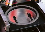
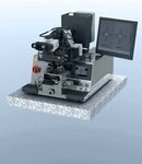
SUSS MJB4 VERSATILE SYSTEM FOR R&D APPLICATIONS AND LOW-VOLUME PRODUCTION - DAYTAM
←
→
Page content transcription
If your browser does not render page correctly, please read the page content below
MJB4
QUALITY MEETS INNOVATION

The MJB4 Mask Aligner from SUSS MicroTec is the per-
fect system for research institutes, universities and small
volume production. Easy to use and compact in size, the
SUSS MJB4 has set industry standards specifically for
processing of small wafers/substrates or pieces and offers
an ideal and cost-effective solution for customers with
limited budgets.

Equipped with a reliable, high precision alignment and high
resolution printing capability in the submicron range the
MJB4 demonstrates a performance unsurpassed by any
other comparable machine. The MJB4 is widely used for
MEMS and optoelectronics applications. It can be configu-
red for UV-Nanoimprint Lithography (UV-NIL) applications
and non-standard substrates such as hybrids, high-fre-
quency components for fragile III-V materials.

                                                              MJB4 HIGHLIGHTS

                                                              + Fast and highly accurate alignment with
                                                                SUSS singlefield or splitfield microscope
                                                              + HR Optics enables high resolution prints down
                                                                to 0.5 μm
                                                              + SUSS MO Exposure Optics (MOEO) for excellent
                                                                light uniformity, customized illumination
                                                                and source mask optimization in a mask aligner
                                                              + The universal optics option (UV250/300/400)
                                                                for fast switching between different wavelengths
                                                              + Wafer and substrate handling up to 100 mm
                                                              + Upgradable with a UV-Nanoimprint Lithography
                                                                toolkit

2
INDUSTRY LEADERSHIP THROUGH R&D AND SMALL VOLUME
PRODUCTION
SUSS MicroTec maintains its market leadership in mask MJB4 offers customized solutions for handling standard
aligner technology based on innovative processes and and non-standard substrates, like fragile compound semi-
technological excellence. The SUSS MJB4 Mask Aligner conductors, glass, foils, as well as warped and drilled sub-
stands for the most versatile and flexible aligner solution strates. Therefore a variety of chucks and mask holders are
available for small scale laboratory applications. available as an option that can be easily adapted to the
process required.
The MJB4 is used for lithography of LED Microfluidics device Piezo motor for MEMS applications
Courtesy: IMSAS, Bremen Courtesy: IMT, University of Neuchatel
Structures with steep sidewalls manufactured Reliable submicron patterning with MJB4 UV-NIL: 50 nm, 70 nm lines and spaces
in 100 to 200 µm thick SU8 resist diffraction reducing optics. 0.6 µm resolution imprinted with MJB4 Mask Aligner
Courtesy: mrt, Berlin at 0.8 µm resist thickness
MICROSCOPES
+ Singlefield Microscope + Splitfield Microscope with + Video Microscope
Cost-effective solution for eye-pieces System with eye-pieces and CCD
alignment of small wafers / Offers the operator a larger field camera system. Combined with
substrates of view, and an easy, simultaneous the splitfield microscope it offers
alignment of mask and wafer also highest alignment accuracy and
at the wafer edge enables a precise alignment check
3MJB4 R&D SOLUTIONS – ALIGNMENT METHODS
KEEPING YOU ON TOP
The SUSS MicroTec commitment to supporting a large TOP SIDE ALIGNMENT (TSA)
number of research and development efforts underscores The MJB4 can be equipped with a manual Top Side Align-
our dedication to providing technological innovation. The ment system.
MJB4 is a cost-effective but highly flexible and efficient
state-of-the-art mask aligner solution for all kinds of R&D INFRARED ALIGNMENT (IR)
applications. It represents an excellent platform for researchers Allows the handling of opaque, IR-transparent materials
to develop new processes and technologies. such as GaAs, InP, Silicon or adhesives, as used for thin
wafer handling or encapsulation applications.
EASY AND QUICK CHANGEOVER
MJB4 allows for extremely quick changeover between dif-
ferent wafer sizes. Only chuck and maskholder need to IR ALIGNMENT SYSTEM
be exchanged, which are easy accessible to the operator.
Trained operators can do the wafer size changeover in less + Infrared light source to be positioned manually
than 5 minutes. + Special IR chucks available
+ Dedicated IR objectives
EASY SOFTWARE + Singlefield (M500 or splitfield (M604)
With its ergonomic operation and its elegant, touch panel video microscopes for wavelengths from
based user interface the MJB4 is very easy to operate and 400 to 1200 nm
only requires minimum operator training.
SMALL FOOTPRINT
In the MJB4 maximum functionality is packaged into mini-
mal space. With a footprint of less than 0.5 m2 the MJB4
requires only minimum cleanroom space.
821 mm
603 mm
4EXPOSURE SYSTEM
DIFFRACTION-REDUCING EXPOSURE OPTICS been designed for UV250, UV300 and UV400 and offers
All SUSS Mask Aligners are using well established diffrac- broadband spectra, based on only one UV lamp.
tion-reducing illumination optics designed to compensa-
te diffraction effects in contact and proximity lithography.
In a SUSS MicroTec Mask Aligner, the photomask is not
just simply illuminated with a plane wave, but with an
annular spectrum of planar waves to reduce higher diffraction
orders. The diffraction reducing exposure optics from
SUSS MicroTec significantly improves resolution and side-
wall profiles.
SUSS Diffraction-Reducing Exposure Optics are available
for the spectral ranges UV400, UV300 and UV250 and are
able to significantly improve resolution and sidewall profiles.
DEDICATED OPTICS SOLUTIONS MO EXPOSURE OPTICS ® (MOEO)
The MJB4 is a full-field exposure system capable of expo- SUSS MO Exposure Optics is based on unique high-quality
sing wafers and substrates up to 100 mm as well as pieces. microlens arrays that are combined with an exchangeable
SUSS MicroTec offers optimized solutions for dedicated Illumination Filter Plate (IFP). These simulate changing
spectral ranges such as UV250, UV300 and UV400 to exposure optics, thus making the use of additional optics
address different resolution requirements. All optics deliver components redundant. MOEO allows customized illumi-
optimum light uniformity of < 3 %. nation through modification of the IFP and enables use of
The combined SUSS broadband optics enables an easy enhanced lithography techniques such as Source-Mask
switch between different applications and wavelengths Optimization (SMO) or Optical Proximity Correction (OPC).
without mechanical changeover. This unique new optics has
Optical system of a
SUSS MJB4 Mask Aligner
5PRINTING MODES
The SUSS MJB4 is capable of handling several exposure
sequences: Soft Contact
Mask
SOFT CONTACT
In soft contact mode the wafer is brought into contact
with the mask and is fixed onto the chuck with vacuum. In Chuck
this exposure mode the MJB4 can achieve a resolution of Vac
2.0 μm. Mechanical pressure
HARD CONTACT
In hard contact mode the wafer is brought in direct contact
with the mask, while positive nitrogen pressure is used to
press the substrate against the mask. In hard contact mode Hard Contact
Mask
a resolution in the 1 micron range is possible.
VACUUM CONTACT FOR HIGH PRECISION
In this mode, a vacuum is drawn between mask and sub-
N2
strate during exposure. This results in a high resolution of
< 0.8 µm. Mechanical pressure
SOFT VACUUM CONTACT
For brittle or fragile substrates a soft vacuum contact
exposure can be performed. The soft vacuum contact Vacuum Contact
exposure mode reduces the vacuum impact to the sub- Mask
strate which leads to a high resolution not achievable in
soft or hard contact. Seal
PROXIMITY PRINTING Vac N2
Although the MJB4 is not considered to be a proximity Mechanical pressure
exposure system, the proximity printing mode allows
exposure at a pre-set gap of up to 50 μm after initial wafer
to mask leveling. This reduces mask damages, especially
for larger feature sizes. MJB4 RESOLUTION
EXPOSURE MODE UV400 UV300 UV250
Vacuum Contact < 0.8 μm < 0.6 μm < 0.5 μm
Hard Contact 1.0 μm < 1.0 μm –
Soft Contact 2.0 μm < 2.0 μm –
Gap Exposure > 3.0 μm
Line, Space resolution achieved in 1 μm thick resist AZ 4110 (UV400, UV300)
and UV6 (UV250) the resolution depends on wafer size, wafer flatness, resist
type, clean room condition and therefore, might vary for different processes.
6MJB4
TECHNICAL DATA
MASK AND WAFER / SUBSTRATE ALIGNMENT STAGE
Wafer Size 1 up to 100 mm / 4" (round) MA Movement Range X: ± 5 mm
Y: ± 5 mm
Max. Substrate Size 100 x 100 mm
Theta: ± 5°
Min. Pieces 5 x 5 mm
Mechanical Resolution X, Y: 0.1 μm
Wafer Thickness Up to 4 mm Theta: 4 x 10⁻⁵°
Mask Size Standard 2" x 2" up to 5" x 5" (SEMI) TOPSIDE MICROSCOPE (TSA)
Mask Thickness Up to 4.8 mm / 190 mil Movement Range X: ± 40 mm
Y: + 30 – 50 mm
EXPOSURE OPTICS
Theta: ± 4°
Contact: soft, hard, vacuum, soft vacuum
UTILITIES
Vacuum contact adjustable to 200 mbar abs
Vacuum < – 0.8 bar < 200 hPa abs
Gap exposure, adjustable gap 10 – 50 µm
Compressed Air 5.5 bar (81 psi)
Flood exposure, split exposure
Nitrogen > 1.5 bar (22 psi)
Lamp control modes: constant power, constant intensity
POWER REQUIREMENTS
EXPOSURE OPTICS
Power Voltage AC 230 V ± 10 %
RESOLUTION
Frequency 50 – 60 Hz
Wavelength Range UV400: 350 – 450 nm (g, h, i-line)
POWER REQUIREMENTS
UV 300: 280 – 350 nm
UV 250: 240 – 260 nm Width x Depth 605 x 810 mm = 0.5 m2
UV 250 / 300 / 400: 240 – 450 nm
Height 660 mm
Exposure Source CPC: Constant Power Controller for lamps
Weight up to 130 kg (290 kg with antivibration table)
Hg 200 W and Hg 350 W
CIC1200: Constant Intensity Controller for Operator Safety and CE-mark, others on request
lamps Ergonomics Sound Pressure Level: < 70 db A)
Hg 200 W, Hg 350 W and HgXE 500 W UV radiation emissions (315 – 400 nm):
(Deep UV) < 0.2 mW / cm
Uniformity Standard: 3.5 %
MO Exposure Optics: 2.5 %
ALIGNMENT METHODS
Top Side Alignment < 0.5 μm (with SUSS recommended wafer
(TSA) Accuracy targets)
Transmitted Infrared < 5 µm (2 µm under special process
Alignment (IR) Ac- conditions)
curacy
Alignment Gap 10 – 50 μm
Data, design and specification of custom-built machines depend on individual process conditions and can vary according to equipment configurations. Not all specifications may be
valid simultaneously. Illustrations in this brochure are not legally binding. SUSS MicroTec reserves the right to change machine specifications without prior notice.
7NORTH AMERICA EUROPE ASIA
USA Germany France Japan China Singapore
Switzerland United Kingdom Korea Taiwan
Headquarters Sites
MJB4 · 10/2018 · BR_ MJB4_ 2018 · V2
Visit www.suss.com/locations
for your nearest SUSS representative or
contact us:
SÜSS MicroTec SE
+49 89 32007-0 . info@suss.com WWW.SUSS.COMYou can also read


