Single-atom sites on perovskite chips for record-high sensitivity and quantification in SERS - Springer
←
→
Page content transcription
If your browser does not render page correctly, please read the page content below
SCIENCE CHINA Materials                                                                                                               ARTICLES
mater.scichina.com link.springer.com                                             Published online 2 March 2022 | https://doi.org/10.1007/s40843-022-1968-5
                                                                                                                Sci China Mater 2022, 65(6): 1601–1614

Single-atom sites on perovskite chips for record-high sensitivity and
quantification in SERS
Ran Feng1†, Qing Miao2†, Xiang Zhang3†, Peixin Cui4†, Cong Wang1*, Yibo Feng1, Liyong Gan3,
Jiaxing Fu6, Shibo Wang7, Ziyi Dai8, Liming Hu5, Yunjing Luo5, Weihai Sun7, Xiaoxian Zhang2,
Jiawen Xiao1, Jinbo Wu6, Bingpu Zhou8, Mingqiang Zou9, Dawei He2, Xiaoyuan Zhou3 and
Xiaodong Han1*

ABSTRACT Surface enhanced Raman scattering (SERS) is a                           INTRODUCTION
rapid and nondestructive technique that is capable of detect-                    Surface enhanced Raman scattering (SERS) has been intensively
ing and identifying chemical or biological compounds. Sen-                       studied for fingerprint tracing of biological and chemical
sitive SERS quantification is vital for practical applications,                  molecules [1], which has a wide variety of applications, such as
particularly for portable detection of biomolecules such as                      in food safety, chemical reaction monitoring and medical
amino acids and nucleotides. However, few approaches can                         diagnostics [2–4]. Regarding the widely-applied and robust
achieve sensitive and quantitative Raman detection of these                      techniques of electrophoresis, fluorescence and chromato-
most fundamental components in biology. Herein, a noble-                         graphy, they usually exhibit ultrasensitive capabilities and
metal-free single-atom site on a chip strategy was applied to                    quantitative linear relationships over a large range from the
modify single tungsten atom oxide on a lead halide perovskite,                   nanomole (single-molecule level) to mole level, which accelerate
which provides sensitive SERS quantification for various                         their applications in various biochemical analyses, including cell,
analytes, including rhodamine, tyrosine and cytosine. The                        protein and nucleic acid analyses [5–7]. However, as a powerful
single-atom site on a chip can enable quantitative linear SERS                   analytical technique, the major weakness of applying SERS in
responses of rhodamine (10−6–1 mmol L−1), tyrosine (0.06–                        biological applications is the low sensitivity to nucleotides and
1 mmol L−1) and cytosine (0.2–45 mmol L−1), respectively,                        amino acids and lack of quantification of Raman scattering
which all achieve record-high enhancement factors among                          signals [3,5]. As the primary and fundamental elements,
plasmonic-free semiconductors. The experimental test and                         nucleotides and amino acids are important biomolecules among
theoretical simulation both reveal that the enhanced me-                         living organisms in most life processes. Amino acids are build-
chanism can be ascribed to the controllable single-atom site,                    ing blocks of proteins that can yield various information, while
which can not only trap photoinduced electrons from the                          nucleotide detection can provide gene information. Although
perovskite substrate but also enhance the highly efficient and                   several analytical methods have quantitative analysis capability,
quantitative charge transfer to analytes. Furthermore, the la-                   the next technological revolution of in-vitro diagnosis (IVD) and
bel-free strategy of single-atom sites on a chip can be applied                  point-of-care testing (POCT) is considered to be fast, direct and
in a portable Raman platform to obtain a sensitivity similar to                  highly sensitive analysis of nucleotides and amino acids with
that on a benchtop instrument, which can be readily extended                     precise structural features [8]. Thus, for SERS, sensitive and
to various biomolecules for low-cost, widely demanded and                        quantitative analysis of amino acids or nucleotide molecules is a
more precise point-of-care testing or in-vitro detection.                        challenging task but of enormous value. Moreover, in the recent
                                                                                 years, the attractiveness of portable Raman instruments for
Keywords: SERS, single-atom site, point-of-care testing, in-vitro                POCT/IVD detection has been significantly growing due to their
diagnosis, charge-transfer mechanism, lead halide perovskite                     portability and economic advantages [9]. These advantages can

1
  Beijing Key Laboratory of Microstructure and Properties of Solids, Institute of Microstructure and Property of Advanced Materials, Faculty of Materials and
  Manufacturing, Beijing University of Technology, Beijing 100124, China
2
  Key Laboratory of Luminescence and Optical Information, Ministry of Education, Institute of Optoelectronic Technology, Beijing Jiaotong University,
  Beijing 100044, China
3
  College of Physics and Center for Quantum Materials and Devices, Analytical and Testing Center, Chongqing University, Chongqing 401331, China
4
  Key Laboratory of Soil Environment and Pollution Remediation, Institute of Soil Science, Chinese Academy of Sciences, Nanjing 210008, China
5
  Faculty of Environment and Life, Beijing Key Laboratory of Environmental and Oncology, Beijing University of Technology, Beijing 100124, China
6
  Materials Genome Institute, Shanghai University, Shanghai 200444, China
7
  College of Materials science and Engineering, Huaqiao University, Xiamen 361021, China
8
  Joint Key Laboratory of the Ministry of Education, Institute of Applied Physics and Materials Engineering, University of Macau, Avenida da Universidade,
  Taipa, Macau 999078, China
9
  Chinese Academy of Inspection and Quarantine (CAIQ), Beijing 100123, China
†
  The authors contributed equally to this work.
*
  Corresponding authors (emails: smartswang@bjut.edu.cn (Wang C); xdhan@bjut.edu.cn (Han X))

June 2022 | Vol. 65 No. 6            © Science China Press and Springer-Verlag GmbH Germany, part of Springer Nature 2022                             1601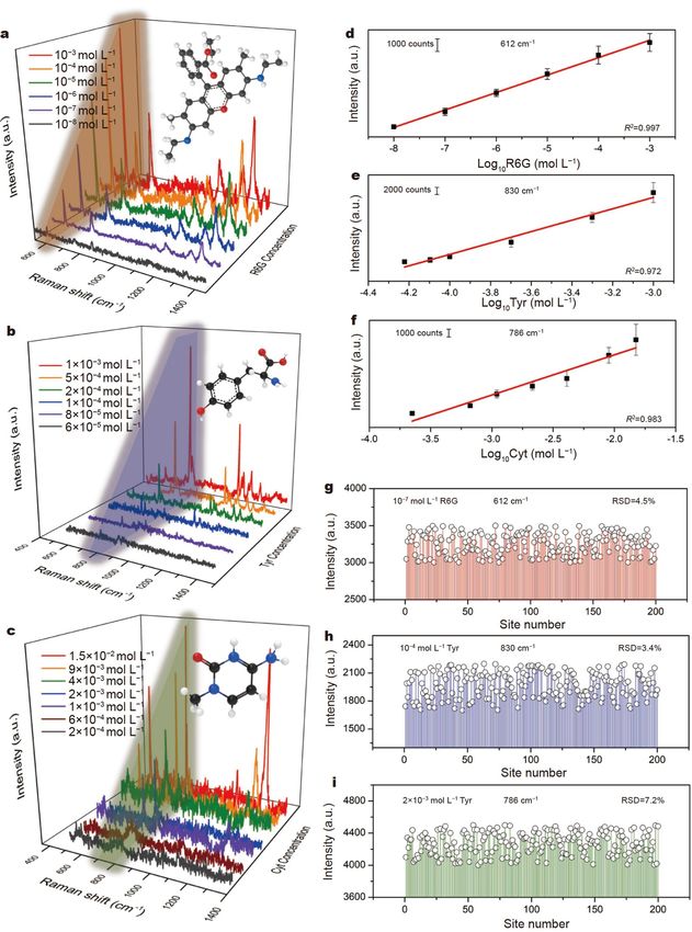
ARTICLES                                                                                                    SCIENCE CHINA Materials
dramatically expand the application of SERS to diagnosis (such                rather than Raman scattering noise. Hence, new guidelines for
as COVID-19), emergency supervision and homeland security                     photoinduced generation of SERS signals from semiconductor
with broad prospects. However, compared with those in con-                    substrates can be further developed by manipulating charge-
ventional Raman confocal setups, the unfocused laser spots and                transfer sites. Moreover, due to that various amino acids or
low-end charge-coupled devices may decrease the sensitivity to                DNA fragments have diverse energy levels, the optimized
analytes, especially for complex biomolecules, which becomes a                semiconductor energy level can potentially provide a suitable
bottleneck for widespread portable Raman application. A highly                band structure for the charge transfer. Coherently, an inorganic-
sensitive, uniform and robust SERS substrate should overcome                  based ternary heterostructure Fe3O4@GO@TiO2 SERS substrate
the weakness of portable Raman spectroscopy and solve this                    was synthesized to obtain remarkable charge-transfer sites via a
problem together.                                                             precise charge-transfer path formed by a tandem nanostructure
   To achieve the sensitive and quantitative analysis of biological           [36]. Besides, an organic semiconductor site for charge transfer
molecules, the SERS substrate has been extensively developed via              has also been proposed and extensively studied [25], leading to a
two main strategies, i.e., high enhancement factor (EF) for high              large SERS EF via a charge-transfer-favorable path and effective
sensitivity and controllable sites for quantification. For high               molecular interactions. Thus, this strategy of tandem charge-
sensitivity, Huang et al. [10] developed an electro-plasmonic                 transfer or novel charge-transfer sites can potentially be applied
method to identify a single amino acid among 20 distinct mul-                 in the design of SERS substrates via nanostructure manipulation
tiplexed amino acid signals on Au nanostars. Kim et al. [11]                  to produce a quantitative and ultrasensitive SERS detection.
successfully designed mildly selective self-assembled monolayers                 Since charge transfer and interactions occur on the sites at the
to capture various DNA or proteins in complex cell lysates on                 several-nanometers level, an in-depth understanding of the
Au substrates. However, since the precise control of electric                 energy level and quantum yield can be more extensively inves-
fields at hotspots is essentially difficult, especially at the atomic         tigated at the atomic scale, which potentially provides a broad
scale, the quantitative SERS based on the electric field faces a              playground for research in this community [1,5]. At the atomic
severe bottleneck for noble-metal-based detection. Although                   scale, sites have recently been intensely investigated to under-
several quantitative analyses have been realized by the accurate              stand the relationship between sites and target molecules [37].
label/tag/condensed techniques on noble metals [12–16], the                   Downsizing sites to the smallest limit is an extensively applied
randomly distributed hotspots lead to considerable uncertainty,               strategy, including single-atom sites, single-atom oxides or
resulting in poor reproducibility of the quantitative SERS signals            ultrathin-layer materials [38–40]. The precise sites and their
on metallic substrates [17,18]. Thus, the discovery of plasmon-               charge-transfer mechanism should be increasingly investigated
free SERS platform via low-cost and scalable approaches is of                 to determine the charge-transfer behavior in terms of thermo-
great interest. In recent years, semiconductor chips/materials                dynamics and kinetics: photoinduced electron generation,
based on another mechanism, the chemical enhancement                          charge-transfer paths and quantum efficiency. Herein, we
mechanism (CM), have attracted more attention for SERS. Due                   developed controllable single-atom oxide sites on semiconductor
to the quantitative formation of charge transfer between the sites            chips, i.e., monodispersed sites of single tungsten atom oxide on
and nearby molecules, quantitative analysis can be mostly                     a lead halide perovskite. The advantage of the design is that the
achieved by semiconductor substrates, such as metallic W18O49,                perovskite is considered as an excellent PL substrate providing
Ta2O5, δ-MoN nanosheets, atomic vacancies/two-dimensional                     sufficient photoinduced charge [41], and a large number of
(2D)-TiO2, ZnO, Ti3C2, conductive polymers [19–25], 2D                        monodispersed sites on the planar perovskite can be applied to
materials [26,27] and metal-organic frameworks (MOFs)                         adsorb probe molecules to obtain reproducible Raman scattering
[28,29]. However, novel semiconductors need to be further                     signals of biological molecules (DNA fragments and amino
explored for superior sensitivity. Enhancement of charge trans-               acids). More importantly, the charge transfer for SERS
fer (quantum yield) on semiconductors for single-molecule level               enhancement can be tuned by the single-atom sites, which can
SERS has drawn considerable attention via further (1)                         quantitatively transfer photoinduced charge and novel energy
improvement of the photoinduced charge generation [30] and                    level for charge transfer. Additionally, considering the advan-
(2) strengthening of the interaction between sites and probe                  tages of single-atom sites on chips, the uniform, low-cost and
biomolecules [17,31–33]. Furthermore, along these two lines, the              large-scale production of novel substrates is beneficial for
understanding of SERS enhancement mechanism could be                          practical SERS applications. Sensitive and quantitative SERS was
greatly deepened and enriched. For instance, as important                     successfully realized on portable Raman instruments. Thus, the
charge-transfer parameters, the quantum yield and lifetime are                single-atom site strategy with precise control of accessible sites
extremely difficult to quantify and are rarely reported. Thus, an             on perovskite chips might open a new platform of sensitive and
in-depth understanding of the charge transfer is required in                  quantitative SERS for practical application, which is urgently
semiconductor SERS, and a universal strategy of semiconductor                 needed in the communities of materials science, environmental
substrate development based on charge transfer is urgently in                 science and biology.
demand.
   Recently, along these two lines, Sun et al. [34] found that SERS           EXPERIMENTAL SECTION
signals can partially originate from the modulated photo-
luminescence (PL) on noble metal, which is different from tra-                Chemicals and materials
ditional cognition that the PL usually causes the undesirable                 All chemicals, including sodium tungstate dihydrate
background of noise in SERS detection due to photon scattering                (Na2WO4·2H2O), hydrochloric acid (HCl), polyethylene glycol
mechanisms [5]. Interestingly, Yang et al. [35] studied the                   (molecular weight MW = 200 Da, abbreviated as PEG-200),
charge-transfer mechanisms on Nd-doped ZnO to further reveal                  ethanol, ethylene glycol (EG), lead bromide (PbBr2), cesium
that PL quenching is correlated with the SERS improvement                     bromide (CsBr), dimethyl sulfoxide (DMSO), rhodamine 6G

1602                              © Science China Press and Springer-Verlag GmbH Germany, part of Springer Nature 2022     June 2022 | Vol. 65 No. 6

SCIENCE CHINA Materials                                                                                                   ARTICLES
(R6G), tyrosine (Tyr), and cytosine (Cyt) were obtained from                surface and excellent photon-to-electron conversion efficiency
Aladdin chemical reagent Corp (Shanghai, China) and employed                [42,43]. Then, single-atom sites can be controllably anchored on
without further purification. Water used in the experiments was             this substrate to obtain quantitative sites. We chose oxygen-
Nanopure water made using a Barnstead Nanopure Diamond                      coordinated tungsten atom as the single-atom site, which can
system.                                                                     have 4–6 coordinated oxygen atoms surrounding the single
                                                                            tungsten atom. More importantly, the single-atom sites of oxy-
Synthesis of CsPb2Br5 (CPB) chip                                            gen-coordinated tungsten atoms have the advantage of highly
PbBr2 solution (21 μL, 1 mol L−1) was spin-coated on an indium              efficient charge transfer [40]. A schematic of the synthesis pro-
tin oxide (ITO) chip at 2000 r min−1 for 30 s and dried on a hot            cess of single-atom sites on chips is shown in Fig. 1a. Photo-
plate at 100°C for 30 min. After cooling to room temperature,               graphy of the flat and uniform chip is shown in Fig. 1a (right).
150 μL CsBr solution (0.07 mol L−1) was spin-coated on the chip             An amplified sandwich-type structure of “ITO glass/perovskite/
at 2000 r min−1 for 30 s and dried on a hot plate at 250°C for              single site” is demonstrated in the cross-section image via
5 min. By repeating this procedure 8 times, high-quality CPB                scanning electron microscopy (SEM) (Fig. 1b). After anchoring
chips were successfully synthesized on ITO.                                 single sites on the perovskite, the perovskite surface remains
                                                                            smooth and neat, as characterized by SEM (Fig. 1c). Elemental
Synthesis of W1–O–CPB chip                                                  mapping via EDS indicates that tungsten (W), cesium (Cs), lead
The synthetic method of single tungsten site precursor is mod-              (Pb) and bromine (Br) are uniformly dispersed on a partial piece
ified upon our previous work [40]. Na2WO4·2H2O (2.27 mmol,                  of the chip at a scale of 10 μm (Fig. 1d). Compared with pristine
750 mg) and PEG-200 (1 mL) were dissolved in deionized water                CPB (Fig. S1, Supplementary information), the SEM image of
(10 mL), stirred for 30 min at ambient temperature, and then                the single sites on perovskite chip (W1–O–CPB) has no obvious
hydrochloric acid (HCl) was added dropwise into the mixture                 morphological changes at μm scale. The X-ray diffraction
until pH 5.5. The obtained solution was magnetically stirred in             (XRD) also shows that the single-atom sites would not induce a
the dark for 6 h. Finally, the as-synthesized CPB chip was first            periodic lattice difference in perovskite (Fig. 1e). Moreover, to
immersed in 30 mL of EG/H2O (1:10) mixture, and then,                       characterize this structure more precisely, the atomic-scale
1200 μL of the as-synthesized W single sites solution was added             morphology of CPB was also verified by HR-TEM. Lattice dis-
to the mixture. The mixture was sealed, heated at 60°C for 1 h,             tances of 0.268 and 0.300 nm represent the (310) and (220)
and then annealed at 80°C for 12 h.                                         facets of the CPB substrate, respectively (Fig. 1f). The single-
                                                                            atom sites of tungsten can be observed in the amplified image
SERS experiments                                                            obtained by HAADF-STEM. The brightness contrast in Fig. 1g
To study the SERS properties of these W1–O–CPB chips, a                     shows that the tungsten atoms are anchored on a planar and thin
confocal micro-Raman spectrometer (RENISHAW inVia) was                      CPB substrate. In addition, the single-atom sites precursor can
used as the measuring instrument. In all SERS tests, unless                 also be identified by HAADF-STEM as shown in Fig. S2. Fur-
specifically stated, the excitation wavelength was 532 nm, the              thermore, the anchored single-atom sites on the perovskite can
laser power was 0.5 mW, and the specification of the objective              induce a valence state change in the substrate (Fig. S3) according
was 50 × L. A series of standard solutions of R6G, Tyr, and Cyt             to X-ray photoelectron spectroscopy (XPS). The Pb valence
at different concentrations were used as the probe molecules.               states have a 1.6 eV upshift, which indicates that Pb (orthor-
Synthesized W1–O–CPB chips were immersed in 1 mL probe                      hombic Pb–O) [44] has a stronger bonding with single sites than
molecule solution at different concentrations for 1 h. The pro-             that in pristine CsPb2Br5 (Pb–Br). In contrast, the valence states
be@W1–O–CPB chips were washed with ethanol and water in an                  of W and Cs exhibit no obvious changes (Fig. S3), and the 1:2
ultrasonic cleaner and dried at 60°C. The portable Raman                    ratio of W5+/W6+ is consistent with that of as-prepared single
experimental conditions were as follows: laser wavelength:                  sites [40]. These results suggest that the Pb atoms on the per-
785 nm; power: 10 mW; acquisition time: 10 s.                               ovskite surface lattice might have bonded with oxygen atoms
                                                                            from the oxygen-coordinated single tungsten atom oxide.
Characterization                                                               To further analyze the configuration of a single-atom site
High-resolution transmission electron microscopy (HR-TEM),                  more thoroughly, the W1–O–CPB was further examined by X-
high-angle annular dark field scanning TEM (HAADF-STEM)                     ray absorption near-edge structure (XANES) and extended X-
and energy-dispersive X-ray spectroscopy (EDS) elemental                    ray absorption fine structure (EXAFS). First, the Fourier-trans-
mapping characterization were performed by a Titan Themis G2                formed (FT) EXAFS spectrum (Fig. 2a, b) shows one main peak
transmission electron microscope operated at 300 kV and                     of W–O at 1.79 Å, in contrast to the W–W coordination peak at
equipped with a probe spherical aberration corrector. Induc-                2.6 Å shown in the W foil, confirming the existence of mono-
tively coupled plasma optical emission spectrometry (ICP-OES)               dispersed atom sites. This is consistent with the HAADF-STEM
measurements were conducted on an Agilent ICP-OES-730                       result that the single-atom sites are randomly dispersed on the
analyzer.                                                                   CPB surface. Furthermore, wavelet-transform EXAFS also
                                                                            indicates the distinct difference between single-atom sites and
RESULTS AND DISCUSSION                                                      reference samples (Fig. 2d–f). In addition, the W LIII-edge
                                                                            XANES spectra were analyzed (Fig. 2c), in which the red-line
Structural characterization of the single-atom sites on chip                peak of W1–O–CPB is located nearby that of WO3, revealing that
To achieve regular chips with controllable sites, we chose the              the presence of W5+ and mainly W6+, similar to the single-atom
well-investigated substrate of a lead halide perovskite (CPB)               oxide precursor with a dominant chemical states of 6+. Addi-
scintillator, which is widely investigated in solar cells and SERS          tionally, the coordinated number of single-atom sites on the
due to its suitable absorption wavelength, highly engineered                perovskite is also steady. Thus, the anchoring process of W1–O–

June 2022 | Vol. 65 No. 6       © Science China Press and Springer-Verlag GmbH Germany, part of Springer Nature 2022                    1603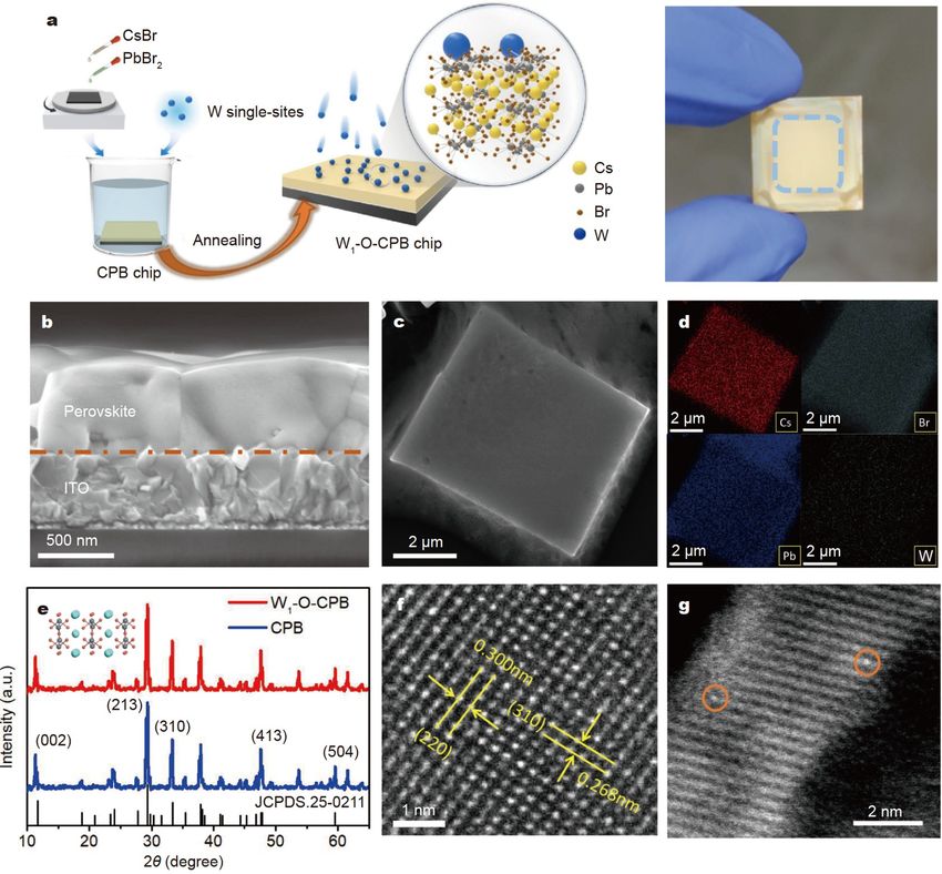
ARTICLES                                                                                                      SCIENCE CHINA Materials

Figure 1 Synthesis and morphological characterization of the W1–O–CPB chip. (a) Schematic illustration of the fabrication of the W1–O–CPB chip (left).
Photography of the W1–O–CPB chip (right). The blue dotted zone of the chip is used for Raman detection. Blue balls represent oxygen-coordinated single
tungsten atoms. (b) Cross-sectional SEM image demonstrating the perovskite film on ITO arrays. (c, d) SEM-EDS images of the W1–O–CPB chip showing the
uniform distributions of Cs, Pb, Br and W elements on the chip. (e) XRD patterns of CPB before and after W loading. (f, g) HAADF-STEM images revealing
the lattice structure of the W1–O–CPB chip and single sites on CPB.

CPB has little impact on the single tungsten atom site. Com-                    respectively. In R6G Raman scattering, as shown in Fig. 3a, the
bining with the XPS, EXAFS and TEM results, the configuration                   R6G on W1–O–CPB demonstrates an R1 peak at 612 cm−1 and
of W1–O–CPB can be proposed to be as follows: the single-atom                   an R2 peak at 772 cm−1 that can be clearly observed and assigned
site is identified as W1–O–Pb, and the connecting oxygen should                 to in-plane and out-of-plane bending motions. Additionally, the
be the coordinated oxygen from single tungsten atom oxide.                      R3 peak at 1362 cm−1 and R4 peak at 1651 cm−1 can be attrib-
Compared with bare single tungsten atom oxide [40], the CPB                     uted to C–C stretching vibrations of the aromatic nucleus. The
substrate might induce a small distortion of the W1–O config-                   significant peak at 612 cm−1 originating from R6G@W1–O–CPB
uration (Fig. 2a and Table 1).                                                  can be observed, as marked by the orange zone (Fig. 3a), to
                                                                                exhibit a linear increase as the R6G concentration increases
Sensitive SERS quantification by the single-atom sites on chip                  (Fig. 3d), with a correlation coefficient of R2 = 0.997. The linear
To demonstrate the SERS activity, a standard probe molecule                     limit of the single-atom sites on a chip can reach 10−9 mol L−1,
(λmol ≈ λlaser = 532 nm), i.e., R6G, was first dissolved in different           which can be calculated as reaching a ultralow level of 60
concentrations for characterization. The representative SERS                    molecules per spot according to the reported procedure [45].
spectra are shown in Fig. 3a. Furthermore, to further extend the                The EF of R6G adsorbed on a single site was calculated to be as
single-atom sites on chip to a universal strategy for biological                high as 107 (see Supplementary information for calculation
molecule detection, the aromatic amino acid Tyr and a single                    details), and a tunable EF is obtained at various probe con-
fragment of the molecule nucleotide Cyt were chosen for ana-                    centrations as shown in Fig. S4. W1–O–CPB has the record-high
lysis (Fig. 3b, c). The quantitative analysis and the relative                  sensitivity among the plasmonic-free substrates and even is
standard deviations (RSDs) are shown in Fig. 3d–f and g–i,                      comparable to the electromagnetic mechanism (EM) dominant

1604                                © Science China Press and Springer-Verlag GmbH Germany, part of Springer Nature 2022      June 2022 | Vol. 65 No. 6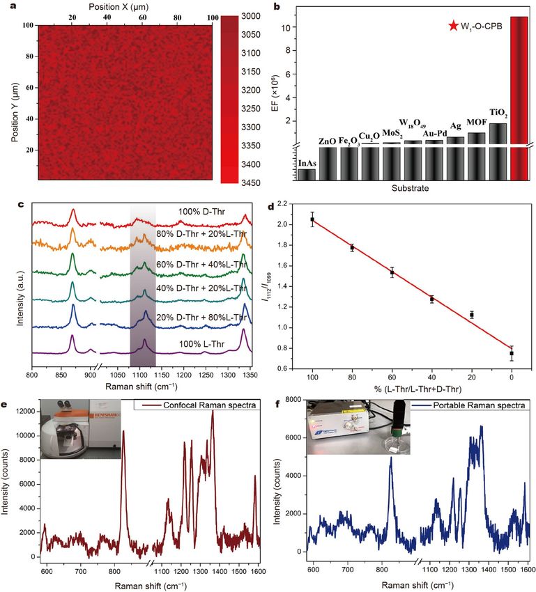
SCIENCE CHINA Materials                                                                                                                  ARTICLES

Figure 2 Atomic configuration of a single-atom site on the perovskite substrate. (a) Comparison of the FT-EXAFS curves between the experimental data and
the fitted spectra of W1–O–CPB. (b, c) Corresponding k3-weighted FT spectra of W1–O–CPB, WO2, WO3 and W foil: (b) the EXAFS spectra, (c) the W LIII-
edge XANES spectra. The last three materials were used as reference samples. (d–f) Wavelet-transform EXAFS of the W1–O–CPB and the reference samples of
W foil and WO3 crystal.

Table 1    EXAFS fitting parameters at the W LIII-edge for various samples (Ѕ02 = 0.896)
          Sample                  Shell                  Na                   R (Å)b                σ2 (Å2)c             ΔE0 (eV)d              R factor
                                 W–O                     2.6                   1.79                 0.0132
      W1–O–CPB                                                                                                               0.4                 0.0241
                               W–O–Pb                    2.1                   2.81                 0.0114
   a) N: coordination number; b) R: bond distance; c) σ2: Debye-Waller factor; d) ΔE0: the inner potential correction. R factor: goodness of fit. Ѕ02 was set to
0.896, according to the experimental EXAFS fit of W foil by fixing CN as the known crystallographic value.

noble metals (single-particle condition). The previously reported                 which is also confirmed by Fourier transform infrared (FTIR)
detection limits in the literature are summarized in Fig. 4b and                  spectroscopy indicating that the –OH group from the surfactant
Table S1. In addition, the reproducibility is confirmed by Raman                  exists on the substrate surface, as shown in Fig. S6. To exclude
mapping of R6G. One hundred runs in triplicate for SERS                           the effect of molecules coordinated with single atoms, FTIR
(Fig. 4a) on a single site provided visual 2D spectral mapping at                 spectroscopy was performed, and the results (Fig. S7a) show that
a concentration of 10−7 mol L−1, and the RSD of I612 was 4.5%                     extra molecules on CPB have been completely removed by
(Fig. 3g), indicating obvious signal reproducibility and relia-                   thermal treatment when the temperature reaches 400°C for 10 h,
bility. The reference samples selected for comparison are bare                    which is below the phase-transition temperature of CPB. Fig.
CPB, bare R6G and R6G@CPB. Fig. S5 illustrates the pristine                       S7b exhibits similar Raman spectra of the sample before and
CPB Raman scattering signals, showing that the inorganic sub-                     after annealing treatment, indicating that the single-atom sites
strate has several weak peaks from ethylene glycol surfactants,                   are contributed by the single metal atom sites rather than only

June 2022 | Vol. 65 No. 6             © Science China Press and Springer-Verlag GmbH Germany, part of Springer Nature 2022                                 1605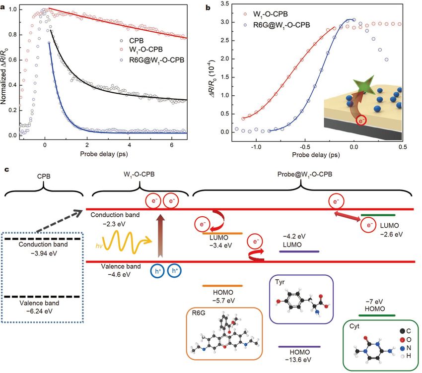
ARTICLES                                                                                                        SCIENCE CHINA Materials

Figure 3 SERS properties of the W1–O–CPB chip. (a–c) Gradually increasing Raman scattering signals recorded from the three analytes at different
concentrations: (a) R6G, (b) tyrosine, (c) cytosine. Calibration curves of the peak intensity versus the logarithmic concentration of analytes: (d) R6G measured
at 612 cm−1; (e) tyrosine measured at 830 cm−1; (f) cytosine measured at 786 cm−1. The top and bottom of the error bar represent the maximum and minimum
peak intensities, respectively. Signal intensity distributions of (g) R6G@W1–O–CPB, (h) Tyr@W1–O–CPB, and (i) Cyt@W1–O–CPB. The SERS spectra were
obtained by averaging three measurements from five randomly chosen spots.

by surface molecules. Furthermore, in contrast to the weak                          The sensitivity and quantification of nucleotides and amino
Raman scattering spectra of pristine CPB and bare R6G                             acids also have similar performances. As shown in Fig. 3b,
(Fig. S8a), the R6G@CPB (Fig. S8b) exhibits a high-intensity                      absorbed tyrosine exhibits a distinct characteristic Raman signal
Raman signal, suggesting strong surface resonance Raman                           for the benzene-ring breathing doublet bending mode with an
scattering. Surprisingly, when anchoring a single site to form                    R1 peak at 860 cm−1 and an R2 peak at 830 cm−1. Notably, the
R6G@W1–O–CPB (Fig. 3a and Fig. S8c), the single sites can                         intensity of the Raman peak at 830 cm−1 was used as a reference
effectively reduce the signal noise of background.                                peak for further research. The asymmetric molecules of tyrosine

1606                                  © Science China Press and Springer-Verlag GmbH Germany, part of Springer Nature 2022            June 2022 | Vol. 65 No. 6

SCIENCE CHINA Materials                                                                                                                ARTICLES
cannot achieve the same limit of detection as R6G due to their                   spectra in saturated conditions, the EFs of both biomolecules on
relatively narrow Raman scattering cross-section and its elec-                   a single site can be enhanced and reach approximately 104. The
tronic structure without resonance SERS, suggesting that more                    limit of detection of these biomolecules also achieves the highest
sensitivity of semiconductors should be further improved to                      sensitivity on semiconductor substrates [46]. More importantly,
detect these important biological molecules. Similar to that of                  linear quantification of amino acids (830 nm−1) and nucleobases
R6G, the quantification of tyrosine is also illustrated in Fig. 3e.              (786 nm−1) is first realized by single-atom sites on a chip among
The linear increase in Raman intensity versus the log con-                       various semiconductors to the best of our knowledge. The RSDs
centration of target tyrosine molecules from 60 μmol L−1 to                      of biomolecules are confirmed, as shown in Fig. 3h, i, to be 3.4%
1 mmol L−1 with an R2 of 0.972 reveals the capability for                        and 7.2%, respectively. Additionally, to further demonstrate the
quantitative analysis. Cytosine could be able to be quantitatively               single-atom sites on chip, the enantioselective discrimination of
detected from 200 μmol L−1 to 15 mmol L−1 with an R2 of 0.983,                   amino acids can also be achieved as shown in Fig. 4c, d. The
as shown in Fig. 3c, f. Compared with bare tyrosine or cytosine                  SERS peaks of L- and D-threonine (Thr) exhibit highly distinct

Figure 4 Stability and sensitivity of the W1–O–CPB chip. (a) SERS mapping at 612 cm−1 of 10−7 mol L−1 R6G adsorbed on the chip. (b) Comparison of the
EFs between W1–O–CPB chip and other substrates, including plasmon-free semiconductors and single-particle noble metals. (c) Normalized SERS spectra of
the mixtures of L-Thr and D-Thr (the contents of L-Thr and D-Thr are changed from 100% to 0%). (d) Calibration curve of the relative intensity ratio of I1112/
I1099 is plotted versus the content of L-Thr (%) in the L- and D-Thr mixture. (e, f) Comparison of tyrosine Raman spectra on W1–O–CPB obtained via portable
Raman and confocal Raman platforms (785 nm excitation).

June 2022 | Vol. 65 No. 6            © Science China Press and Springer-Verlag GmbH Germany, part of Springer Nature 2022                              1607

ARTICLES SCIENCE CHINA Materials
spectral discrepancies, which may be due to the tendency of pristine CPB and R6G@CPB, whose lifetimes are summarized in
chiral isomers. Surprisingly, plotting the difference in the ratio Table 2. This suggests that single-atom sites on CPB provide new
of the relative intensities of the peaks at 1112/1099 cm−1 against energy levels for charge transfer to adsorbed R6G.
the L-Thr content (in %) reveals a linear correlation with a To further confirm this charge transfer between W1–O–CPB
coefficient of R2 = 0.989. and the probe molecules, their interaction was measured by
Moreover, this single site on chip substrate can overcome the ultraviolet visible (UV-Vis) spectra as shown in Fig. 5d. The W1–
weaknesses of discrepancies of surface sites and low-quantum- O–CPB substrate has a similar absorption as pristine CPB, and
efficiency of photoinduced charges, so that it can be applied in the R6G molecules on single-atom sites of W1–O–CPB exhibit a
portable Raman instruments. Fig. 4e, f show a comparison of the 7-nm redshift compared with that of bare R6G. This reveals that
Raman spectra of Tyr (10−3 mol L−1) on W1–O–CPB obtained charge transfer between the single sites and probe molecules
via a portable Raman platform (785 nm) and a confocal Raman induced by the CM exists at single-atom sites on chip. Con-
platform (785 nm). The similar limits of detection indicate that sistently, Fig. S8 also shows that the Raman peaks of R6G at
the uniform and highly efficient charge-transfer substrate can be single sites have a different spectrum compared with that of bare
broadly applied in practical Raman instruments. Additionally, R6G, supplementarily indicating that the semiconductor-mole-
the long-term stability of R6G on a single site was verified by the cule interaction at the molecule/substrate interface was changed
SERS detection after probe adsorption on chips for six months by single-atom sites. To further reveal the charge transfer and
(Fig. S9), which might be ascribed to the chips effectively adsorption upon single-atom sites decoration on CPB, density
transferring the photoinduced holes away on ITO to avoid functional theory (DFT) calculations were performed to inves-
photooxidation [47]. Dispersed nanomaterials may have pho- tigate the spatial charge redistributions between the R6G
toinduced analyte structural damage caused by photobleaching molecule and CsPb2Br5 (001), as shown in Fig. 5e–g. The pos-
and/or metal-catalyzed side reactions, which is a severe draw- sible configurations were considered as a single site coordinated
back of the conventional SERS substrates [48]. Chips with with Pb atoms, as shown in Fig. 5e. Clearly, the charge redis-
layered structures can provide a promising approach for por- tribution is more remarkable on modified surfaces (0.26 e− from
table SERS activity in food safety, environmental protection and W1–O–CPB to R6G vs. 0.16 e− from bare CPB to R6G), which is
biological detection, which can balance the trade-off among the consistent with experimental evidence of increased molecular
numerical aperture of spectrometers, the transmittance or polarizability. Furthermore, the plane-averaged electron density
reflectivity of the optical elements, and the noise of charge- of CPB before and after single-atom site decoration is visualized
coupled devices [49]. in Fig. S10b, which might be induced by the distortion of CPB
upon single-atom site anchoring. Hence, incorporation of sin-
SERS mechanism of the single-atom sites on chip gle-atom sites gives rise to remarkable charge increase at the
Due to the plasmon-free nature of single-atom sites and CPB surface region, implying a higher ability to donate charges to the
semiconductors, CMs are mainly considered, including charge molecule. Thus, the calculations clearly demonstrated that the
generation, charge transfer and interaction between probes and unique advantage of single-atom sites is effective improvement
sites, which are related to three features of single sites on chips: of the interfacial charge transfer and thus the magnified mole-
PL quenching, enhanced charge transfer and quantitative cular polarization.
adsorption of probes. Notably, in addition to the static coupling of the analyte and
single-atom site, to directly verify highly efficient charge transfer
PL quenching and enhanced charge-transfer mechanism from single sites to probe, photocarrier kinetics were studied by
Generally, photoinduced carriers are beneficial for SERS and the a transient absorption technique by probing the nonresonant
trapping of carriers from photoluminescent substrates can photon intensity induced by a laser pulse with a central wave-
effectively reduce the noise caused by resonance Raman scat- length of 530 nm. Fig. 6a shows the obtained transient absorp-
tering [5]. Quantitative PL quenching and charge transfer are tion decay spectra of various samples (CPB, W1–O–CPB,
important issues in the photoinduced process. First, perovskite R6G@W1–O–CPB), and the exciton decay follows the bi-expo-
substrates are well known for their PL performance with ultra- nential model with τ1 (fast decay) and τ2 (slow decay) (detailed
high photoelectron quantum efficiency (over 40%), and it has data in Table 3). The short time constant of τ1 (0.89 and
been investigated as an SERS substrate with an EF of 104–5 13.44 ps) can be attributed to fast processes associated with
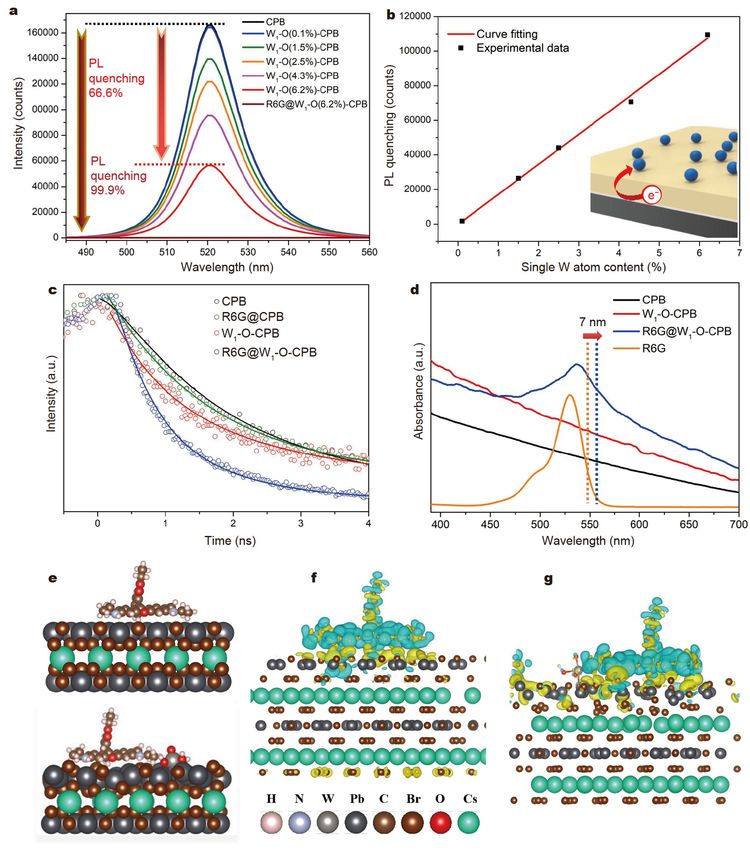
[43,50]. Fig. 5a demonstrates the gradually reduced PL intensity exciton formation: the free carriers injected by the pump pulse
with the following sequence as: CPB, W1–O–CPB, R6G@W1–O– can induce a differential reflection signal more effectively than
CPB. Moreover, the tunable PL quenching is shown as the the excitons through the screening effect. Hence, the slow decay
density of single-atom sites (Table S2 measured by ICP-OES) of τ2 is attributed to the exciton lifetime. Compared with pristine
increase as shown in Fig. 5b. The PL quenching can be quan- CPB, the single-atom site on the CPB chip can significantly
tified, showing that the quantum yield of charge transfer from extend the lifetime from 22.99 to 83.16 ps, which indicates that
CPB to single sites is approximately ~66%. The reduced PL is single-atom sites can effectively trap the photoinduced electrons
also beneficial for avoiding the resonance from the substrate PL, from CPB. Interestingly, when probe R6G is adsorbed onto the
which is usually considered as the Raman noise. Regarding the single sites, the lifetime is remarkably reduced to 0.52 ps, sug-
R6G@CPB with a high resonance noise (Fig. S8b), the strategy of gesting that the trapped electron can be transferred to probe
single-atom sites on perovskite chips can provide effective PL molecules through the single-atom site pathway. Moreover, the
quenching, which results in not only elimination of background photoinduced electron transfer process was analyzed based on
noise but also charge transfer. To further reveal the PL Fig. 6b and Table 3. First, the red circles show that the signal in
quenching in terms of kinetics, Fig. 5c shows that W1–O–CPB W1–O–CPB rapidly rises. The red curve over the data represents
has a shorter lifetime and a specific decay process compared with the integral of a Gaussian function with a full width at half
1608 © Science China Press and Springer-Verlag GmbH Germany, part of Springer Nature 2022 June 2022 | Vol. 65 No. 6
SCIENCE CHINA Materials                                                                                                                 ARTICLES

Figure 5 Mechanism of the absorption and charge-transfer process on the W1–O–CPB chip. (a) PL spectra of W1–O–CPB with various single-atom sites
density (0–6.2 wt%) and that of R6G@W1–O–CPB. (b) Linear relationship between PL quenching counts and single-atom sites density. Inserted schematic
shows the charge transfer from CPB to a single W site. (c) Transient PL spectra of R6G@W1–O–CPB compared with W1–O–CPB, R6G@CPB and bare CPB.
(d) UV-Vis absorption spectra of R6G@W1–O–CPB compared with R6G. (e) Side view of configuration of R6G@CPB and R6G@W1–O–CPB for DFT
simulation. The green, dark gray, brown, light gray, red and pink balls represent Cs, Pb, Br, W, O and H atoms, respectively. (f) Charge density difference for
R6G adsorption on pristine CPB, and (g) single-atom site modified CsPb2Br5 (001). Yellow and cyan regions correspond to charge accumulation and
depletion, respectively. The iso-surface value is 0.0003 electrons Å−3.

Table 2 Parameters settings and data analysis of transient PL spectra             maximum of 0.7 ps. Such an ultrafast transfer can be ascribed to
(excitation wavelength: 395 nm, emission wavelength: 520 nm)                      a newly formed energy level induced by the single-atom sites, in
           Sample                Exposure time (s)            τ (ns)              which subpicosecond interlayer charge transfer is generally
             CPB                      102.48                  1.686               obtained. Since the charge transfer time is much longer than the
                                                                                  photoinduced electron lifetime, the majority of the electrons
         W1–O–CPB                     494.89                  1.285
                                                                                  excited in CPB are effectively transferred to the single-atom sites.
         R6G@CPB                      127.64                  1.597               Furthermore, when R6G is adsorbed on W1–O–CPB, the rising
      R6G@W1–O–CPB                    131.24                  0.593               time corresponds to a width of 0.43 ps, as shown by the blue-

June 2022 | Vol. 65 No. 6             © Science China Press and Springer-Verlag GmbH Germany, part of Springer Nature 2022                              1609
ARTICLES                                                                                                     SCIENCE CHINA Materials

Figure 6 Photoinduced charge transfer of single-atom site on perovskite. (a) Transient absorption spectra of R6G@W1–O–CPB compared with W1–O–CPB
and CPB. (b) The blue curve and red curve are the fitting to the charge-induced transfer processes of W1–O–CPB and R6G@W1–O–CPB, with transfer times
of 0.70 and 0.43 ps, respectively. Inserted schematic shows the charge transfer between CPB and the single site with analyte molecules. (c) Schematic
illustration of the energy levels and photoinduced charge transfer of pristine CPB, W1–O–CPB, R6G, tyrosine, and cytosine.

circled curve in Fig. 6b, which suggests that the electron transfer            transfer to the probe molecule at the single-atom sites or nearby.
on the R6G@W1–O–CPB is faster than that on W1–O–CPB. This                      The photoinduced charge transfer sequence is “CPB–single-
may be due to that the formation of new electronic states on                   atom site–analyte”: (i) first, photoinduced electrons are gener-
single-atom sites may interact with lowest unoccupied molecular                ated from the perovskite substrate; (ii) then, they are transferred
orbital (LUMO) of the probe molecule, where electrons take a                   to single-atom sites; (iii) finally, they interact with the target
new pathway in the transfer process. This result is consistent                 molecules. The unique photoinduced charge transfer relies on a
with the transient PL results (Fig. 5c). Combining with these                  single-atom site with high charge-transfer capability. Moreover,
steady-state (PL and absorption) and time-resolved (PL and                     according to the Herzberg-Teller selection rule, charge-transfer
absorption) spectra, direct evidence of charge transfer from the               processes resonant with incident light selectively enhance dif-
CPB substrate to single-atom sites and further to probe mole-                  ferent modes of probe molecules, and quantitative charge
cules is presented, resulting in much enhanced SERS activity.                  transfer might determine the quantitative signals based on the
Moreover, the quantum yield of charge transfer via single-atom                 specific symmetric vibrational modes of probe molecules [51].
sites can be revealed, which involves not only quenching of                    Compared with absorption under 532 nm excitation, an obvious
~66% of photoinduced carriers in steady-state but also shows an                decline (~44%) in the Raman intensity was observed under
areal carrier density from single-atom sites to analytes as sum-               633 nm irradiation (Fig. S11), while small Raman signals were
marized in Table 3.                                                            obtained under 785 nm (Fig. S11). The results indicate that
   The corresponding band structure (Fig. 6c) of single-atom                   specific resonance from the band diagram plays an important
sites on perovskite indicated that the photoinduced charge                     role in Raman enhancement, and the Raman spectra of the
transfer involves PL quenching of the substrate and charge                     adsorbed molecules strongly depend on the energy of the inci-

1610                               © Science China Press and Springer-Verlag GmbH Germany, part of Springer Nature 2022      June 2022 | Vol. 65 No. 6
SCIENCE CHINA Materials                                                                                                              ARTICLES
Table 3    Parameters settings and data analysis of the transient absorption spectra
                                                                            Absorption coefficient        Areal carrier density      Charge transfer
       Sample                  τ1 (ps)                   τ2 (ps)                    (m−1)                    (× 1014 m−2)a             time (ps)b
          CPB               0.887 ± 0.031           22.992 ± 0.618                 283,410.1                     4.1801                     –
    W1–O–CPB                13.441 ± 0.450          83.164 ± 4.578                 248,847.9                     3.4829                    0.70
 R6G@W1–O–CPB                     –                 0.52597 ± 0.005                248,847.9                     2.9464                    0.43
  a) Carrier density calculation details are given in the Supplementary information; b) charge transfer data are shown in Fig. S13. Pump wavelength 410 nm,
probe wavelength 520 nm.

dent light. To illustrate the charge-transfer process in terms of                 calculated as 7.647 × 10⁸ per 7.85 × 10⁻¹³ m2 (within a laser spot,
the thermodynamics, a band structure is drawn containing bare                     detailed in Supplementary information), indicating that the
CPB, W1–O–CPB and probe molecules (Fig. 6c and Fig. S12).                         number of capture sites is sufficient for analyte detection at
The locations of the valence band maximum (VBM) of CPB and                        single molecule level. Further addition of single-atom sites
W1–O–CPB were measured, and their energy levels of VBM are                        would cause the rough morphology and distortion of the per-
−6.24 and −4.6 eV, respectively (Fig. S12a–c). According to the                   ovskite chip (Fig. S13a–c) compared with the smooth surface
UV-Vis absorption spectra (Fig. S12b, c), the bandgaps of CPB                     (Fig. 1b–c). The surface variation of sites might result in poor
and W1–O–CPB are approximately near 2.3 eV, and their con-                        reproducibility. Meanwhile, the adsorption is essentially driven
duction band minimum (CBM) levels should be at −3.94 and                          by electrostatic Coulomb force between the surface areas with
−2.3 eV. This is consistent with the simulated density of states of               single-atom sites and probe molecules due to their distinctively
W1–O–CPB having an upshift compared with that of CPB                              positive and negative charges (Table S3). Fig. S14a shows a
(Fig. S10a). Together with previously reported data on R6G,                       uniform dispersion of R6G on single-atom sites anchored chip,
amino acids and nucleobases [52], the highest occupied mole-                      whereas the pristine chip with the same concentration of R6G
cular orbital (HOMO) and LUMO for R6G, tyrosine, and                              has obviously lower loading, as shown in Fig. S14b, suggesting
cytosine are −5.7/−3.4, −13.6/−4.2 and −7.0/−2.6 eV, respec-                      that the single sites could act as capture sites on the surface.
tively. Hence, the charge transfer is illustrated as red arrows in                Fig. S14a–d also show a gradual increase in adsorbed R6G as the
Fig. 6c. This result is also consistent with W1–O–CPB having an                   density of single-atom sites increases. Table S3 further verifies
electron trapping capability and a lower energy level than the                    the positive zeta potentials of various molecules, and the nega-
CBM of CPB.                                                                       tive zeta potential of W1–O–CPB gradually increases as the
   According to the Herzberg-Teller vibrational coupling law,                     single-atom sites loading amount increases on the perovskite.
molecular resonances caused by the photoinduced charge                            The reason might be that single-atom sites can form –OH on the
transfer greatly enhance the polarization tensor of molecules,                    surface to exhibit negative potentials. Thus, as the probe mole-
correspondingly increasing the Raman scattering cross-section.                    cules in certain pH environments can exhibit positive potentials,
Given that the wavelength of the excitation lasers used in Raman                  the perovskite with the highest loading of single-atom sites
measurement was 532 nm, which is close to the PL peak of the                      exhibits the largest quantitative range in SERS activity (Fig. S15).
CPB substrate, the high EF value would be strongly related to the                 Additionally, the variations in the charge transfer amount for
photoinduced enhancement effect of the CPB substrate (λsub ≈                      different molecules can also be ascribed to various electrophilic
λlaser). In addition, excited electrons can also be induced by                    abilities of functional groups [53].
probes. For the R6G molecule, whose bandgap is very close to                         According to the classic adsorption model [54], the relation-
the excitation wavelength (532 nm), resonance SERS also con-                      ship between the concentration (C) in the system and the
tributes to the charge-transfer process [19]. The three resonances                number (N) of adsorbents on the surface exhibits a “log(C-N)”
(molecular resonance, photoinduced charge transfer and charge                     quasi-linear curve following the Freundlich adsorption isotherm:
transfer in semiconductors) involved in SERS do not work                          q = kfCn, where q is the adsorption density, C is the dissolved
independently. Consistently, as shown in Fig. S11, when the                       concentration of the adsorbate, and kf and n are empirical
excitation wavelength is changed from 532 to 633 nm, the                          constants. For the Freundlich isotherm, the log-log version is
relative intensities of the 612 and 773 cm−1 peaks of R6G con-                    used: logqe = logkf + 1/nlogC.
siderably decrease, suggesting that the dominant charge transfer                     Hence, we chose the highest loading of single-atom sites to
induced by 633 nm irradiation (1.95 eV) is different from that                    detect Raman scattering of the various molecules, including
induced by 532 nm irradiation. This might result in higher limit                  dyes, amino acids and DNA fragments. The Raman scattering
of detection concentrations for nucleobases and amino acids                       signals of Fig. 3d–f all exhibit a quasi-linear relation with logC,
with larger bandgaps.                                                             suggesting that the adsorbed molecules near the sites are
                                                                                  involved in the resonance Raman intensity (I). The “log(C-(N)-
Single-atom site quantification mechanism                                         I)” relationship is also consistent with other quantitative studies
The quantification mechanism of single-atom sites on chips is                     on dye probe molecules. Additionally, the experimental
revealed to involve two main aspects: quantitative sites and                      adsorption is demonstrated to be physical adsorption on sites via
probe adsorption on the site or nearby. The quantitative amount                   multiple-time and long-term washing experiments (see Supple-
of single sites on chips can be tuned from 0 to ~6 wt% through                    mentary information), showing that the Raman signals of R6G
alteration of the anchoring of single-atom sites, as confirmed by                 have no obvious changes (Fig. S16). Hence, the strategy of sin-
ICP-OES as shown in Table S2. Under the condition of ~6 wt%                       gle-atom sites on chip can provide quantitative capture sites,
loading of single-atom sites, the coverage of sites can also be                   which is a universal approach through nonspecific Coulomb

June 2022 | Vol. 65 No. 6             © Science China Press and Springer-Verlag GmbH Germany, part of Springer Nature 2022                             1611
ARTICLES SCIENCE CHINA Materials
force following the nonselective adsorption rule in SERS. substrate has a result on a portable Raman instrument similar to
that on a benchtop confocal Raman instrument due to the suf-
Discussion ficient photoinduced charge density. Therefore, a sensitive SERS
The substrate materials in SERS are indispensable for ultra- quantification platform can be built based on the strategy of
sensitive detection of biomolecules. Our experimental results single-atom sites on chips, which paves the way for novel
clearly demonstrated that single-atom sites enabled ultrahigh material design for SERS in IVD and POCT.
sensitivity to biomolecules, which can be ascribed to the charge
transfer capability and the favorable energy level, leading to the Received 11 January 2022; accepted 12 January 2022;
significant magnification of molecular polarization and published online 2 March 2022
remarkable enhancement of Raman scattering. Notably, photo- 1 Cardinal MF, Vander Ende E, Hackler RA, et al. Expanding applica-
induced electron separation of the perovskite materials can tions of SERS through versatile nanomaterials engineering. Chem Soc
realize nearly 100% quantum efficiency, which is much higher Rev, 2017, 46: 3886–3903
than those of other semiconductors. Thus, the perovskite 2 Garcia-Rico E, Alvarez-Puebla RA, Guerrini L. Direct surface-enhanced
materials are great candidates for this strategy. Recently, per- Raman scattering (SERS) spectroscopy of nucleic acids: From funda-
ovskites have been studied to achieve a higher EF [43,50]. Our mental studies to real-life applications. Chem Soc Rev, 2018, 47: 4909–
strategy of single-atom sites on chips provides a new route to 4923
3 Bell SEJ, Charron G, Cortés E, et al. Towards reliable and quantitative
discover various sites with satisfactory localized charges to
surface-enhanced Raman scattering (SERS): From key parameters to
achieve robust sensitive SERS with various extensions, including good analytical practice. Angew Chem Int Ed, 2020, 59: 5454–5462
portable Raman detection for POCT/IVD. The single-atom sites 4 Wang X, Huang SC, Hu S, et al. Fundamental understanding and ap-
on chips also exhibit quantitative and reproducible SERS plications of plasmon-enhanced Raman spectroscopy. Nat Rev Phys,
detection, which is determined by controllable sites with new 2020, 2: 253–271
mechanisms. The advantage of single-atom sites on chip can be 5 Langer J, Jimenez de Aberasturi D, Aizpurua J, et al. Present and future
summarized as (1) generating sufficient charge from high-effi- of surface-enhanced Raman scattering. ACS Nano, 2020, 14: 28–117
6 Li D, Yao D, Li C, et al. Nanosol SERS quantitative analytical method:
ciency PL substrate to probe molecules, (2) providing a charge-
A review. TrAC Trends Anal Chem, 2020, 127: 115885
transfer path, and (3) offering certain active sites for adsorption. 7 Jin Y, Xie Y, Wu K, et al. Probing the dynamic interaction between
Meanwhile, the SERS quantification on other semiconductors damaged DNA and a cellular responsive protein using a piezoelectric
should have the similar features. For example, MOFs and car- mass biosensor. ACS Appl Mater Interfaces, 2017, 9: 8490–8497
bon-based organic semiconductors [25,28,29,55] have served as 8 Perales-Rondon JV, Colina A, González MC, et al. Roughened silver
successful candidates with the advantages of high-density cap- microtubes for reproducible and quantitative SERS using a template-
ture sites and quantitative interactions. Nevertheless, the limit of assisted electrosynthesis approach. Appl Mater Today, 2020, 20: 100710
detection is still far from the noble metal hotspot-based sub- 9 Pilot R. SERS detection of food contaminants by means of portable
Raman instruments. J Raman Spectrosc, 2018, 49: 954–981
strates, and the mechanism of the adsorption is usually missing,
10 Huang JA, Mousavi MZ, Giovannini G, et al. Multiplexed dis-
which is a prerequisite for quantification. Single-atom sites crimination of single amino acid residues in polypeptides in a single
strategy can give more precise configurations to study the SERS hot spot. Angew Chem Int Ed, 2020, 59: 11423–11431
adsorption model, such as a single layer or a single cluster. 11 Kim M, Ko SM, Lee C, et al. Hierarchic interfacial nanocube assembly
Single-atom sites prove that the sites can control the site density, for sensitive, selective, and quantitative DNA detection with surface-
site electrophilicity and electronic states, which should be further enhanced Raman scattering. Anal Chem, 2019, 91: 10467–10476
investigated to achieve a more suitable substrate for biological 12 Yan W, Yang L, Chen J, et al. In situ two-step photoreduced SERS
molecule detection. materials for on-chip single-molecule spectroscopy with high re-
producibility. Adv Mater, 2017, 29: 1702893
13 Chen G, Dai Z, Ji B, et al. Dynamic enrichment of plasmonic hot-spots
CONCLUSIONS and analytes on superhydrophobic and magnetically functionalized
High sensitivity and reproducible quantification in SERS platform for surface-enhanced Raman scattering. Sens Actuat B-Chem,
detection are successfully achieved by modifying a single-atom 2020, 319: 128297
site of tungsten atom oxide on lead halide perovskite chips. 14 Wu Y, Bennett D, Tilley RD, et al. How nanoparticles transform single
Through the noble-metal-free single-site strategy, quantitative molecule measurements into quantitative sensors. Adv Mater, 2020, 32:
detection at the ultralow level was successfully realized for R6G 1904339
15 Li JF, Zhang YJ, Ding SY, et al. Core-shell nanoparticle-enhanced Ra-
down to 10−9 mol L−1, which is more sensitive than plasmon-free
man spectroscopy. Chem Rev, 2017, 117: 5002–5069
semiconductors in the literature by at least one order of mag- 16 Xu D, Teng F, Wang Z, et al. Droplet-confined electroless deposition of
nitude. More importantly, a single site on a chip can provide silver nanoparticles on ordered superhydrophobic structures for high
quantitative linear SERS responses from 60 μmol L−1 to uniform SERS measurements. ACS Appl Mater Interfaces, 2017, 9:
10 mmol L−1 (saturated) for biological amino acid detection and 21548–21553
from 200 μmol L−1 to 45 mmol L−1 for nucleotide detection, 17 Kim N, Thomas MR, Bergholt MS, et al. Surface enhanced Raman
which are the highest EFs among semiconductors to the best of scattering artificial nose for high dimensionality fingerprinting. Nat
our knowledge. The mechanism of superior SERS is ascribed to Commun, 2020, 11: 207
18 Lee HK, Lee YH, Koh CSL, et al. Designing surface-enhanced Raman
the controllable single sites, which not only provide quantitative scattering (SERS) platforms beyond hotspot engineering: Emerging
sites for analyte adsorption but also enhance the charge transfer opportunities in analyte manipulations and hybrid materials. Chem Soc
by effectively trapping photoinduced electrons from the sub- Rev, 2019, 48: 731–756
strate and transporting them to the analytes. Consistently, the PL 19 Yang L, Peng Y, Yang Y, et al. A novel ultra-sensitive semiconductor
quenching and charge-transfer sequence of single-atom sites is SERS substrate boosted by the coupled resonance effect. Adv Sci, 2019,
revealed to be “perovskite–single-atom site–analyte” by simula- 6: 1900310
tion and experimental results. Moreover, this highly efficient 20 Cong S, Yuan Y, Chen Z, et al. Noble metal-comparable SERS en-
1612 © Science China Press and Springer-Verlag GmbH Germany, part of Springer Nature 2022 June 2022 | Vol. 65 No. 6You can also read