Silicon electronic-photonic integrated 25 Gb/s ring modulator transmitter with a built-in temperature controller
←
→
Page content transcription
If your browser does not render page correctly, please read the page content below
Research Article                                                                     Vol. 9, No. 4 / April 2021 / Photonics Research   507

Silicon electronic–photonic integrated 25 Gb/s
ring modulator transmitter with a built-in
temperature controller
MINKYU KIM,1 MIN-HYEONG KIM,1,2 YOUNGKWAN JO,1 HYUN-KYU KIM,1                                              STEFAN LISCHKE,3
CHRISTIAN MAI,3 LARS ZIMMERMANN,3,4 AND WOO-YOUNG CHOI1,*
1
  Department of Electrical and Electronic Engineering, Yonsei University, 03722 Seoul, Republic of Korea
2
  Current address: Samsung Electronics, Hwasung, 18448 Gyeonggi-do, Republic of Korea
3
  IHP, Im Technologiepark 25, 15236 Frankfurt (Oder), Germany
4
  Technische Universität Berlin, Einsteinufer 25, 10587 Berlin, Germany
*Corresponding author: wchoi@yonsei.ac.kr

Received 27 October 2020; revised 18 January 2021; accepted 2 February 2021; posted 2 February 2021 (Doc. ID 413407);
published 22 March 2021

      We demonstrate a silicon electronic–photonic integrated 25 Gb/s nonreturn-to-zero transmitter that includes
      driver circuits, depletion-type Si ring modulator, Ge photodetector, temperature sensor, on-chip heater, and
      temperature controller, all monolithically integrated on a 0.25 μm photonic BiCMOS technology platform.
      The integrated transmitter successfully provides stable and optimal 25 Gb/s modulation characteristics against
      external temperature fluctuation. © 2021 Chinese Laser Press
      https://doi.org/10.1364/PRJ.413407

1. INTRODUCTION                                                           the controller monitors the amount of transmission at the res-
Si photonic transmitters based on ring resonators are very attrac-        onance wavelength where the transmitted optical power is either
tive since they have small footprint, energy-efficient operation,         minimum or maximum, making the controller implementation
and large modulation bandwidth. With these, they are expected             relatively straightforward. However, because the RM input wave-
to replace Si Mach–Zehnder modulators that are presently                  length providing the maximum optical modulation amplitude
widely used in the data center interconnect applications [1–3].           (OMA) is away from the resonance wavelength [18], realizing
In addition, Si ring modulators (RMs) with their wavelength-              a temperature control technique that determines and maintains
dependent characteristics can provide a very large data through-          the optimal temperature for the RM can be challenging. In Refs.
put capability with wavelength division multiplexing (WDM),               [12–14], the average modulated optical power is monitored and
as schematically shown in Fig. 1. Consequently, they attract a            locked to a set value with a closed-loop feedback. However, this
great amount of research interest for next-generation optical in-         set value must be externally supplied. In Ref. [15], the RM OMA
terconnect solutions that are needed for high-performance                 is directly monitored by high-speed sampling of the designated
computing systems [4]. Furthermore, ring-resonator-based pho-             modulation pattern with slope quantization. But high-speed
tonic switches are expected to play an important role for next-           sampling consumes a large amount of power, especially when
generation photonic switching systems [5].                                the data rate is high. OMA maximization based on bit statistics
    Ring resonator characteristics, however, are highly sensitive         using the training data sequence can achieve low-power opera-
to temperature. For example, just a one degree temperature                tion [16], but maintaining the optimal condition when the tem-
change can significantly degrade the modulation eye quality,              perature changes from the initial calibration condition may
as shown in Fig. 2, where measured transmission characteristics           require additional calibration steps.
and 25 Gb/s eye diagrams are shown for a sample Si RM at                      To alleviate the problems discussed above, we have previ-
two different temperatures with a fixed input wavelength.                 ously reported a custom-designed temperature control IC with
Consequently, a technique to maintain the correct temperature             which the optimal temperature for the RM OMA is automati-
for optimal device performance is a necessity for any application         cally determined in the calibration mode and is stably main-
of ring-resonator-based devices, including Si RMs. There are              tained in the lock mode with a 1-bit dithering technique
several previously reported temperature control (TC) tech-                [17]. This approach, however, requires continuous OMA mon-
niques for ring resonator filters [6–9], switches [10,11], and            itoring in the lock mode, resulting in increased power con-
modulators [12–17]. For resonator-based filters and switches,             sumption. In this paper, we present what we believe, to the

2327-9125/21/040507-07 Journal © 2021 Chinese Laser Press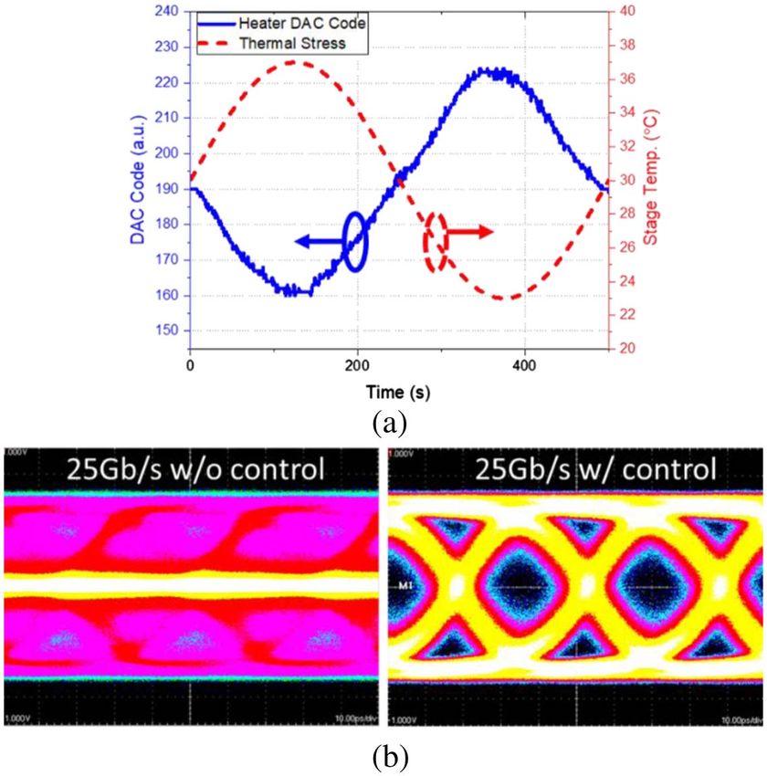
508 Vol. 9, No. 4 / April 2021 / Photonics Research Research Article
Fig. 1. Block diagram of the silicon photonic WDM transmitter
with ring resonators.
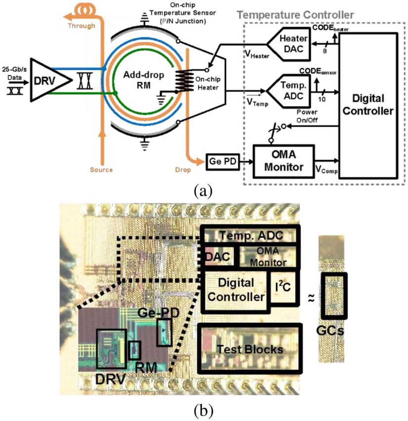
Fig. 3. (a) Block diagram and (b) fabricated chip photo of the
monolithic silicon photonic transmitter with a temperature controller.
fabricated chip. It consists of an electronic driver, RM, Ge
monitoring PD, on-chip heater, on-chip temperature sensor,
and temperature controller. The driver amplifies externally sup-
Fig. 2. Measured transmission curves and 25 Gb/s eye diagrams for plied 25 Gb∕s 0.6V pp,diff NRZ data and delivers 3V pp,diff to
different temperatures. the Si depletion-type RM. The driver consists of two-stage am-
plifiers, as shown in Fig. 4. The first stage is designed so that it
can buffer input electrical signals before they are delivered to
best of our knowledge, is a new approach in which the OMA the second stage, which has large-size transistors. It employs the
monitoring block is used only in the calibration mode. This is RC degeneration technique that provides bandwidth enhance-
achieved using an on-chip temperature sensor [19]. With this, ment by reducing gain in the low-frequency range [22]. The
the controller can determine and remember the optimal RM second stage uses the differential cascode structure so that it
temperature in the calibration mode, and maintain this temper- can generate 3V pp,diff swing without any transistor breakdown.
ature in the lock mode. In this paper, we explain how our tem- The output signals of the second stage are delivered to the RM
perature control technique works and provide measurement with capacitive coupling so that desired RM bias voltages can
results based on a 25 Gb/s Si photonic transmitter IC realized be supplied. To design these amplifiers, electronic–photonic
on the photonic BiCMOS technology platform [20], which co-simulation with the newly developed large-signal SPICE
contains monolithically integrated photonic and electronic model for the RM [23,24] is used so that the driver load re-
components. sistance (R L ) in the second stage can be optimized for both
This paper is organized in four sections. In Section 2, we
describe the details of our monolithically integrated Si photonic
transmitter along with explanations for the temperature control
algorithm. In Section 3, the measurement results for our trans-
mitter are given. Finally, Section 4 concludes the paper. The
initial results of this work were reported in Ref. [21], but in
this paper, we provide significantly more detailed explanations
for our transmitter and the temperature control algorithm is
given. Furthermore, the experimental results that verify the sta-
ble operation of our transmitter against the larger temperature
stress range (from 5°C to 15°C) are presented.
2. RM TRANSMITTER WITH TC CIRCUIT
Figure 3(a) shows the block diagram of our custom-designed
Si photonic transmitter IC and Fig. 3(b) is a photo of the Fig. 4. Schematic of the RM driver circuits.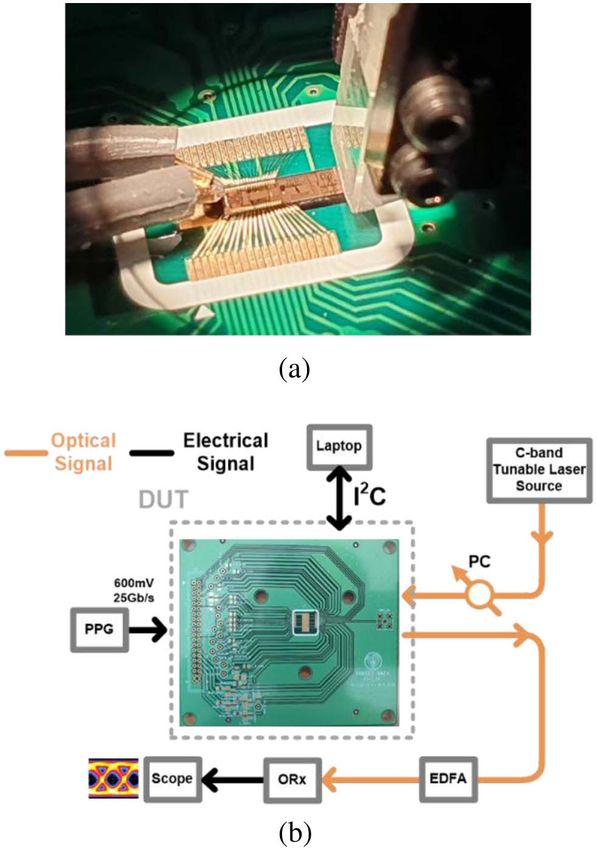
Research Article Vol. 9, No. 4 / April 2021 / Photonics Research 509
power consumption and the RM output optical eye perfor- replica circuit, V temp represents the voltage across the PN junc-
mance. The power consumption of such a driver IC tion at a given RM temperature corresponding to I REF . The
is 329 mW. voltage difference between the V bias and V temp is amplified
The RM has 12 μm radius and is made up of 500 nm wide and converted to a 10-bit digital code (CODEsensor ).
waveguides implemented on the standard Si photonic SOI Figure 7 shows the timing diagram for the temperature con-
structure. An optical drop port is added to the RM so that trol operation, which is divided into two modes: the calibration
OMA can be directly monitored with an integrated Ge PD, mode and the lock mode. In the calibration mode, the control-
as shown in Fig. 3(a). An N-doped Si heater is placed within ler provides increasing voltages (V Heater ) to the on-chip heater
the ring waveguide, which can change the RM temperature up through the heater DAC output digital codes (CODEheater ) so
to 40% of its 8.293 nm free spectral range (FSR). PN-junction- that the RM temperature can be scanned in the pre-determined
based temperature sensors are placed above and below range. With this, the RM OMA (V OMA ) changes as the RM
the RM, which provide voltage signals representing the RM modulation characteristics change with changing temperature.
temperature. Simultaneously, the RM temperature is monitored with the
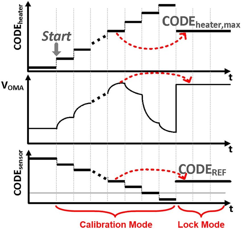
The temperature controller has four building blocks: an temperature ADC output code (CODEsensor ). After the scan
OMA monitor, an ADC for temperature sensor output, a is complete, the digital controller determines the maximum
DAC for on-heat heater driving, and a digital controller, as OMA and the temperature at which the maximum OMA is
shown in Fig. 3(a). The OMA monitor contains a transimpe- achieved and stores them as CODEheater, max and CODEREF .
dance amplifier (TIA) with a 40 dBΩ gain and a 20 GHz band- This approach can reduce the power consumption a lot since
width, plus a power detector, track-and-hold (T/H) circuit, and the OMA block is turned off at the lock mode; however, it
a comparator, as shown in Fig. 5 [17]. Modulated optical sig- cannot track the laser wavelength due to its aging or environ-
nals from the drop port of the RM are converted into electrical ment. If such a change occurs, a higher-level control is required
signals and amplified with the monitor Ge PD and the TIA, in which the RM is recalibrated.
and the power detector produces V OMA representing RM In the lock mode, the heater voltage is set to the value de-
OMA. With the T/H and the comparator, V comp is produced, termined to produce the maximum OMA in the calibration
which represents the latest and largest value of V OMA so that mode. Then, to maintain the maximum OMA against any tem-
V OMA is continuously updated during the calibration mode. perature perturbation, a PID control is applied to the heater
Figure 6 shows the temperature sensor ADC, which con- voltage so that the optimum RM temperature is maintained.
verts the voltage signals across the PN junctions near the The OMA monitor block is turned off in the lock mode so
RM at a fixed current into a 10-bit digital code. This block that power can be saved. The on-chip digital controller is
is composed of a reference replica circuit, an amplifier, and implemented by synthesis based on a 0.25 μm CMOS standard
a second-order Σ − Δ modulator ADC [25]. The temperature library provided by the IHP Photonic BiCMOS technology
sensor has 0.2°C/LSB sensitivity with a maximum range of and is composed of more than 2000 transistors.
50°C. With the reference current (I REF ) determined in the Figure 8 shows the simulated results for the temperature
control operation. For this simulation, the temperature-
dependent characteristics of the RM, the on-chip heater,
and the on-chip temperature sensor are first measured, and
their behavior models are implemented with Verilog-A, a hard-
ware description language. Then, Verilog-A simulation is per-
formed that can account for behaviors of the entire analog and
Fig. 5. Schematic of the OMA monitor block.
Fig. 6. Schematic of the temperature sensor ADC. Fig. 7. Timing diagram for the temperature control operation.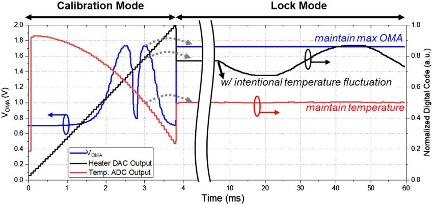
510     Vol. 9, No. 4 / April 2021 / Photonics Research                                                      Research Article

Fig. 8. Simulation results for the temperature control operation with Verilog-A behavior models.

digital circuits as well as the RM, the on-chip heater, and the
temperature sensor. As shown in Fig. 8, with the sweeping
heater DAC code, the RM OMA and the temperature ADC
code change widely. Two temperature conditions are found
for the maximum RM OMA since the RM transmission char-
acteristic is symmetric around the resonance wavelength, as can
be seen in Fig. 2. The digital controller is programmed to take
the latter one. As shown in the figure, the controller correctly
determines the RM temperature and the heater voltage that
produce the maximum OMA in the calibration mode, and
maintains the maximum OMA and the corresponding RM
temperature by modifying the heater voltage when the RM
temperature fluctuation is intentionally introduced in the lock
mode.

3. MEASUREMENT RESULTS
Figure 9(a) shows a photo for the chip under probing, and
Fig. 9(b) shows the block diagram for the measurement setup.
The chip is mounted on an FR4 PCB, and supply and bias
voltages are provided through bonding wires. NRZ data
(0.6V pp,diff , 25 Gb/s PRBS 231 –1) are delivered to the chip
with direct RF probing. Grating couplers are used for photonic
I/O. The RM output optical signals are amplified with an
EDFA, and an optical receiver along with an electric oscillo-
scope is used for the eye measurement. The RM has a near
6 dB loss at the operation point. The transmitter IC contains
                                                                        Fig. 9.   (a) Photo and (b) block diagram of the measurement setup.
an I2 C bus, which externally controls the IC as well as monitors
internal signals such as the DAC and ADC codes during
the measurement. In the calibration mode, the temperature
sensor consumes 2.6 mW, and the OMA monitor block con-                  the increasing heater power, the resonance wavelength shifts
sumes 6.325 mW. On the other hand, high-speed TIA con-                  to the larger wavelength. With the maximum heater power
sumes most of the power: 5.075 mW. The digital controller               of 20.7 mW, which is limited by the allowed maximum supply
consumes only 725 μW. Since the OMA monitor block is                    voltage to the heater DAC in the photonic BiCMOS technol-
only used for the calibration mode and most of the operation            ogy, the resonant wavelength shift of 3.27 nm is possible, which
will be in the lock mode, the total power consumption for               corresponds to a temperature change of 45° or 40% of the RM
the temperature control is 3.325 mW, excluding the heater               FSR at room temperature. Therefore, the TC IC cannot main-
power.                                                                  tain the optimal RM temperature if the resonant wavelength is
    Figure 10 shows the measured RM transmission character-             not within such range. However, the on-chip heater efficiency
istics with different amounts of on-chip heater powers. With            and the temperature tuning range can be greatly improved with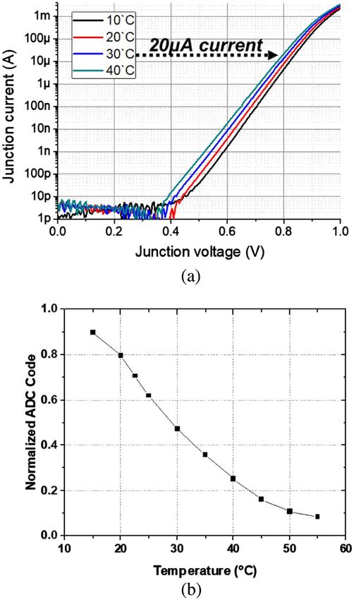
Research Article Vol. 9, No. 4 / April 2021 / Photonics Research 511
characteristics of the PN junction sensors at different temper-
atures. As shown in Fig. 6, the voltage at the PN junction is
determined to generate the reference current (I REF ), which is
set to 20 μA for our measurement. For this measurement, the
stage temperature on which our transmitter IC is placed is
changed. Figure 11(b) shows the resulting ADC codes delivered
to the digital controller.
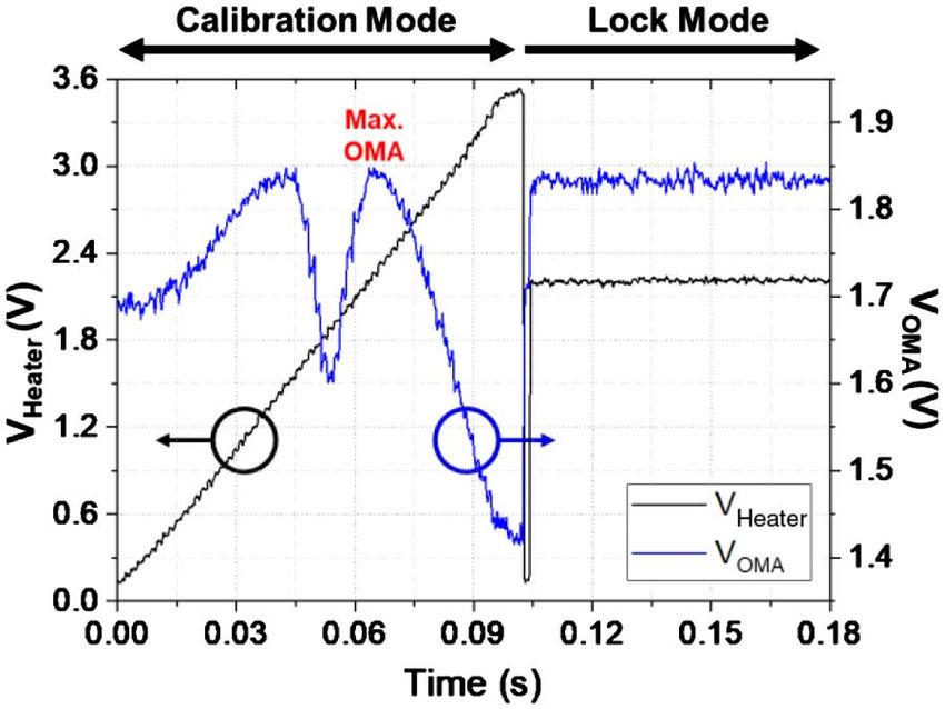
Figure 12 shows the measurement results for heater voltage
(V Heater ) and RM OMA (V OMA ) in the calibration and lock
modes. The heater voltage is scanned with 13 mV resolution
for a 1-bit digital code, resulting in a significant amount of the
RM OMA changes. It can be clearly observed that the digital
controller correctly determines the heater voltage for the maxi-
mum RM OMA and maintains it in the lock mode.
Figure 13(a) shows the measurement results in the lock
mode when the RM goes through a sinusoidal thermal stress
Fig. 10. Measured transmission curve of the RM with different
on-chip heater powers.
better heater fabrication technology [26] and/or the thermal
isolation technique [27,28].
Figure 11 shows the measurement results for the tempera-
ture sensing block. Figure 11(a) shows current-voltage (I-V)
Fig. 12. Measurement results for heater voltage (V Heater ) and RM
OMA (V OMA ) in calibration and lock modes.
Fig. 11. (a) Measured I-V curve for the temperature sensor and Fig. 13. Measurement results in the lock mode with thermal stress
(b) measured ADC output code with different temperatures. showing (a) heater voltage (V Heater ) and (b) 25 Gb/s eye diagrams.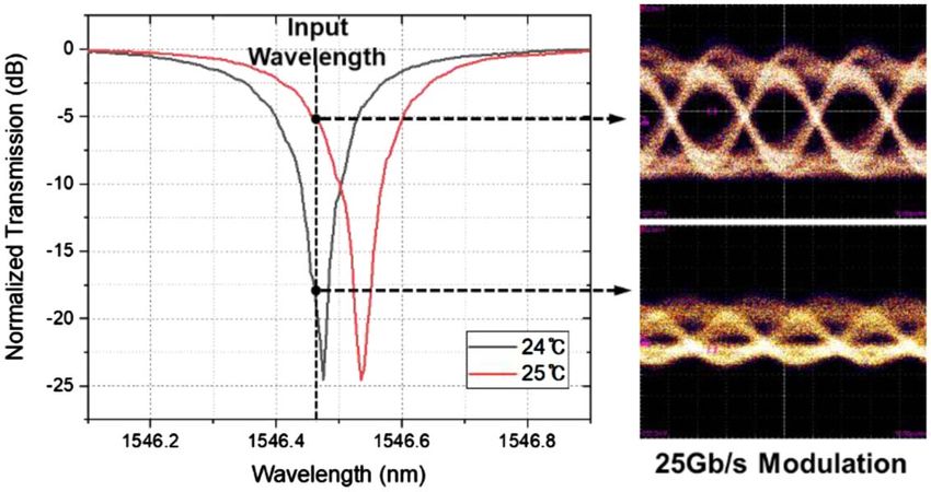
512      Vol. 9, No. 4 / April 2021 / Photonics Research                                                              Research Article

Table 1. Performance Comparison for Silicon Photonic Transmitters with Ring Modulators and Temperature Controllers
                           15 0 JSCC      18 0 ISSCC              20 0 ISSCC        16 0 JSSC         16 0 JSSC            19 0 JLT
                              [12]            [13]                    [14]            [15]              [16]                 [17]          This Work
Process                  130 nm SOI 100 nm SOI               SiPh + 28 nm          130 nm SOI        45 nm                0.25 μm           0.25 μm
                        SiPh + 65 nm SiPh + 65 nm               CMOS              SiPh + 40 nm      CMOS SOI              BiCMOS            Photonic
                           CMOS         CMOS                                         CMOS                                                   BiCMOS
Wavelength                 1550 nm         1310 nm                 1310 nm          1550 nm           1180 nm              1550 nm          1550 nm
Data Rate                      25 Gb/s      10 Gb/s               112 Gb/s           2 Gb/s            5 Gb/s              25 Gb/s           25 Gb/s
Driver                    Yes (Wire-     Yes (3D face-           Yes (3D face-     Yes (Wire-          Yes                    No             Yes
Integration                bonded)          to-face)                to-face)        bonded)         (Monolithic)                          (Monolithic)
Controller               No (Off-chip    Yes (3D face-           Yes (3D face-    No (Off-chip         Yes                    No             Yes
Integration                  PD)            to-face)                to-face)         DAC)           (Monolithic)        (Off-chip PD)     (Monolithic)
Scheme                  Average power Analog closed-          Normalized          OMA monitor       Bit-statistics      OMA monitor           OMA
                                      loop w/digital         average power           w/slope-                            with power          monitor
                                         reconfig.            stabilization        quantization                          detector &            with
                                                                                                                         without step      temperature
                                                                                                                          approach          sensing &
                                                                                                                                           PID control
Manual Reference                 Yes          Yes                    Yes               No                No                   No               No
Setting
Resonance                       N/A           N/A             Not reported            5 nm             2.5 nm              0.55 nm           3.27 nm
Wavelength                                                   (50 mW power
Tuning Range                                                   dissipation)
Temp. Controller           0.17 mW         0.15 mW               Not reported       2.9 mW            0.72 mW             3.91 mW          3.325 mW
Powera
  a
      Excluding heater power

of 15°C with a 500 s period. For the thermal stress, the stage                   sensor, a monitor Ge PD, and analog and digital temperature
temperature is intentionally changed where the PCB contain-                      controllers. With two-step calibration and lock mode opera-
ing the transmitter IC is, as shown by the red dotted line in the                tions, our transmitter can automatically determine the temper-
figure. The blue line shows the internal heater DAC code rep-                    ature at which the RM has the maximum OMA and maintain
resenting voltages applied to the on-chip heater. As the stage                   this condition against any temperature fluctuation. Our tem-
temperature changes, the digital controller changes the heater                   perature control scheme is energy efficient and does not depend
voltage so that the RM remains at the same temperature as                        on the details of RM data rates. With complete monolithic in-
the temperature determined to provide the maximal OMA                            tegration of photonic and electronic components achieved with
in the calibration mode. Figure 13(b) shows the accumulated                      the photonic BiCMOS technology, our transmitter can provide
eye diagrams during this thermal stress for 8 min with and                       the reduced transmitter size as well as the smaller I/O pin num-
without temperature control. The eye remains open with                           bers. We also believe that our approach based on photonic and
5.2 dB extinction ratio even if the stage temperature changes                    electronic integration can be applied to other photonic devices
up to 15°C; however, the eye completely closes without control.                  that require temperature control for best performance.
   Table 1 compares the performance of our transmitter IC
with recently reported RM temperature control ICs. As can                        Funding. Ministry of Trade, Industry and Energy
be seen in the table, only in Ref. [16] and the present work,                    (10065666); National Research Foundation of Korea
the temperature controller can determine the RM optimal tem-                     (2020R1A2C201508911); Yonsei University.
perature without any external reference and monolithic integra-
tion is achieved. The power consumption reported in Ref. [16]                    Acknowledgment. The authors thank the IC Design
is much smaller than our result, which is due to the much ad-                    Education Center (IDEC) for EDA tool support.
vanced SOI CMOS technology used in Ref. [16], not the tem-
perature control algorithm employed. It should also be noted                     Disclosures. The authors declare no conflicts of interest.
that our temperature control scheme does not depend on the
data rate as schemes like in Ref. [15].
                                                                                 REFERENCES
4. CONCLUSION                                                                    1. W. Bogaerts, P. de Heyn, T. van Vaerenbergh, K. de Vos, S. Kumar
                                                                                    Selvaraja, T. Claes, P. Dumon, P. Bienstman, D. van Thourhout, and
We present a fully integrated Si photonic transmitter contain-                      R. Baets, “Silicon microring resonators,” Laser Photon. Rev. 6, 47–73
ing a high-speed RM with an on-chip heater and a temperature                        (2012).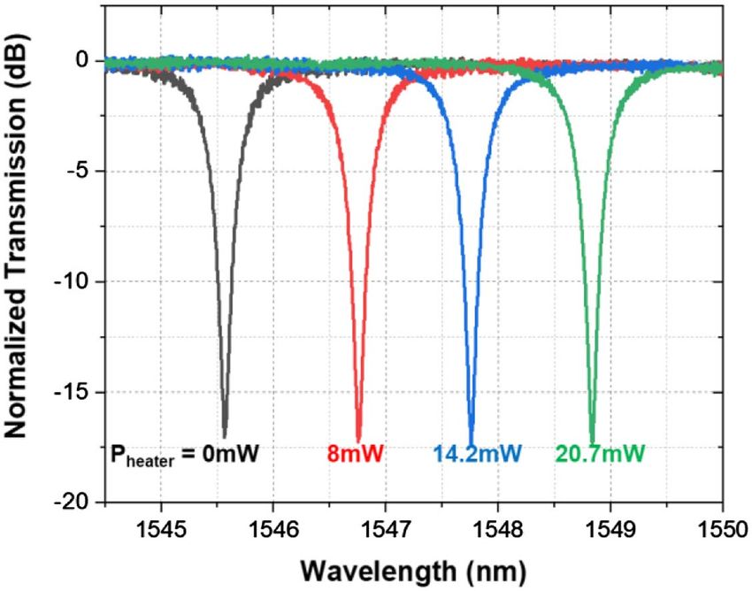
Research Article                                                                            Vol. 9, No. 4 / April 2021 / Photonics Research           513

 2. G. Li, A. V. Krishnamoorthy, I. Shubin, J. Yao, Y. Luo, H. Thacker, X.               112 Gb/s PAM-4 silicon-photonic transmitter with integrated nonlinear
    Zheng, K. Raj, and J. E. Cunningham, “Ring resonator modulators in                   equalization and thermal control,” in IEEE International Solid-State
    silicon for interchip photonic links,” IEEE J. Sel. Top. Quantum                     Circuits Conference (IEEE, 2020), pp. 208–210.
    Electron. 19, 95–113 (2013).                                                   15.   S. Agarwal, M. Ingels, M. Pantouvaki, M. Steyaert, P. Absil, and J. Van
 3. H. Li, B. Casper, G. Balamurugan, M. Sakib, J. Sun, J. Driscoll, R.                  Campenhout, “Wavelength locking of a Si ring modulator using an in-
    Kumar, H. Jayatilleka, H. Rong, and J. Jaussi, “A 112 Gb/s PAM4 sil-                 tegrated drop-port OMA monitoring circuit,” IEEE J. Solid-State
    icon photonics transmitter with microring modulator and CMOS                         Circuits 51, 2328–2344 (2016).
    driver,” J. Lightwave Technol. 38, 131–138 (2020).                             16.   C. Sun, M. Wade, M. Georgas, S. Lin, L. Alloatti, B. Moss, R. Kumar,
 4. C. Sun, M. T. Wade, Y. Lee, J. S. Orcutt, L. Alloatti, M. S. Georgas,                A. H. Atabaki, F. Pavanello, J. M. Shainline, J. S. Orcutt, R. J. Ram, M.
    A. S. Waterman, J. M. Shainline, R. R. Avizienis, S. Lin, B. R. Moss, R.             Popovic, and V. Stojanovic, “A 45 nm CMOS-SOI monolithic photon-
    Kumar, F. Pavanello, A. H. Atabaki, H. M. Cook, A. J. Ou, J. C. Leu,                 ics platform with bit-statistics-based resonant microring thermal tun-
    Y.-H. Chen, K. Asanović, R. J. Ram, M. A. Popović, and V. M.                         ing,” IEEE J. Solid-State Circuits 51, 893–907 (2016).
    Stojanović, “Single-chip microprocessor that communicates directly             17.   M.-H. Kim, L. Zimmermann, and W.-Y. Choi, “A temperature controller
    using light,” Nature 528, 534–538 (2015).                                            IC for maximizing Si micro-ring modulator optical modulation ampli-
 5. Y. Shen, X. Meng, Q. Cheng, S. Rumley, N. Abrams, A. Gazman, E.                      tude,” J. Lightwave Technol. 37, 1200–1206 (2019).
    Manzhosov, M. S. Glick, and K. Bergman, “Silicon photonics                     18.   H. Yu, D. Ying, M. Pantouvaki, J. Van Campenhout, P. Absil, Y. Hao,
    for extreme scale systems,” J. Lightwave Technol. 37, 245–259                        J. Yang, and X. Jiang, “Trade-off between optical modulation ampli-
    (2019).                                                                              tude and modulation bandwidth of silicon micro-ring modulators,” Opt.
 6. K. Padmaraju, D. F. Logan, T. Shiraishi, J. J. Ackert, A. P. Knights,                Express 22, 15178–15189 (2014).
    and K. Bergman, “Wavelength locking and thermally stabilizing micro-           19.   S. Saeedi and A. Emami, “Silicon-photonic PTAT temperature sensor
    ring resonators using dithering signals,” J. Lightwave Technol. 32,                  for micro-ring resonator thermal stabilization,” Opt. Express 23,
    505–512 (2014).                                                                      21875–21883 (2015).
 7. H. Jayatilleka, K. Murray, M. Á. Guillén-Torres, M. Caverley, R. Hu,           20.   D. Knoll, S. Lischke, A. Awny, and L. Zimmermann, “(Invited) SiGe
    N. A. F. Jaeger, L. Chrostowski, and S. Shekhar, “Wavelength tuning                  BiCMOS for Optoelectronics,” ECS Trans. 75, 121–139 (2016).
    and stabilization of microring-based filters using silicon in-resonator        21.   M. Kim, M.-H. Kim, Y. Jo, H.-K. Kim, S. Lischke, C. Mai, L.
    photoconductive heaters,” Opt. Express 23, 25084–25097 (2015).                       Zimmermann, and W.-Y. Choi, “A fully integrated 25 Gb/s Si ring
 8. J. C. C. Mak, W. D. Sacher, T. Xue, J. C. Mikkelsen, Z. Yong, and                    modulator transmitter with a temperature controller,” in Optical
    J. K. S. Poon, “Automatic resonance alignment of high-order microring                Fiber Communication Conference (OSA, 2020), paper T3H.7.
    filters,” IEEE J. Quantum Electron. 51, 0600411 (2015).                        22.   B. Razavi, Design of Integrated Circuits for Optical Communications
 9. K. Yu, C. Li, H. Li, A. Titriku, A. Shafik, B. Wang, Z. Wang, R. Bai, C.-H.          (Wiley, 2012).
    Chen, M. Fiorentino, P. Y. Chiang, and S. Palermo, “A 25 Gb/s hybrid-          23.   M. Kim, K. Park, W.-S. Oh, C. Mai, S. Lischke, L. Zimmermann, and
    integrated silicon photonic source-synchronous receiver with micro-                  W.-Y. Choi, “A 4 × 25-Gbps monolithically integrated Si photonic
    ring wavelength stabilization,” IEEE J. Solid-State Circuits 51,                     WDM transmitter with ring modulators,” in IEEE Optical
    2129–2141 (2016).                                                                    Interconnects Conference (OI) (IEEE, 2019), pp. 1–2.
10. R. Enne, M. Hofbauer, N. Zecevic, B. Goll, and H. Zimmermann,                  24.   M. Kim, M. Shin, M.-H. Kim, B.-M. Yu, Y. Kim, Y. Ban, S. Lischke, C.
    “Integrated analogue-digital control circuit for photonic switch matri-              Mai, L. Zimmermann, and W.-Y. Choi, “Large-signal SPICE model for
    ces,” Electron. Lett. 52, 1045–1047 (2016).                                          depletion-type silicon ring modulators,” Photon. Res. 7, 948–954
11. Z. Zhu, A. Gazman, D. Gidony, Y. Shen, K. Shepard, and K. Bergman,                   (2019).
    “Single-wire DAC/ADC control and feedback of silicon photonic ring             25.   M. A. P. Pertijs, K. A. A. Makinwa, and J. H. Huijsing, “A CMOS smart
    resonator circuits for wavelength switching,” in Optical Fiber                       temperature sensor with a 3σ inaccuracy of 0.1°C from 55°C to
    Communication Conference (OSA, 2018), paper W2A.32.                                  125°C,” IEEE J. Solid-State Circuits 40, 2805–2815 (2005).
12. H. Li, Z. Xuan, A. Titriku, C. Li, K. Yu, B. Wang, A. Shafik, N. Qi, Y. Liu,   26.   M. Pantouvaki, S. A. Srinivasan, Y. Ban, P. De Heyn, P. Verheyen, G.
    R. Ding, T. Baehr-Jones, M. Fiorentino, M. Hochberg, S. Palermo, and                 Lepage, H. Chen, J. De Coster, N. Golshani, S. Balakrishnan, P.
    P. Y. Chiang, “A 25 Gb/s, 4.4 V-swing, AC-coupled ring modulator-                    Absil, and J. Van Campenhout, “Active components for 50 Gb/s
    based WDM transmitter with wavelength stabilization in 65 nm                         NRZ-OOK optical interconnects in a silicon photonics platform,” J.
    CMOS,” IEEE J. Solid-State Circuits 50, 3145–3159 (2015).                            Lightwave Technol. 35, 631–638 (2017).
13. Y. Thonnart, M. Zid, J. L. Gonzalez-Jimenez, G. Waltener, R. Polster,          27.   P. Dong, W. Qian, H. Liang, R. Shafiiha, D. Feng, G. Li, J. E.
    O. Dubray, F. Lepin, S. Bernabe, S. Menezo, G. Pares, O. Castany, L.                 Cunningham, A. V. Krishnamoorthy, and M. Asghari, “Thermally tun-
    Boutafa, P. Grosse, B. Charbonnier, and C. Baudot, “A 10 Gb/s Si-                    able silicon racetrack resonators with ultralow tuning power,” Opt.
    photonic transceiver with 150 μW 120 μs-lock-time digitally super-                   Express 18, 20298–20304 (2010).
    vised analog microring wavelength stabilization for 1 Tb/(s·mm) 2              28.   I. Shubin, X. Zheng, H. Thacker, S. S. Djordjevic, S. Lin, P. Amberg, J.
    die-to-die optical networks,” in IEEE International Solid-State                      Lexau, K. Raj, J. E. Cunningham, and A. V. Krishnamoorthy, “All solid-
    Circuits Conference (IEEE, 2018), pp. 350–352.                                       state multi-chip multi-channel WDM photonic module,” in IEEE 65th
14. H. Li, G. Balamurugan, M. Sakib, R. Kumar, H. Jayatilleka, H. Rong,                  Electronic Components and Technology Conference (ECTC) (IEEE,
    J. Jaussi, and B. Casper, “12.1 A 3D-integrated microring-based                      2015), pp. 1293–1298.
You can also read


