Quantification of Trace-Level Silicon Doping in AlxGa1-xN Films Using Wavelength-Dispersive X-Ray Microanalysis
←
→
Page content transcription
If your browser does not render page correctly, please read the page content below
Microscopy and Microanalysis (2021), 27, 696–704
       doi:10.1017/S1431927621000568

       Original Article

       Quantification of Trace-Level Silicon Doping in AlxGa1–xN Films Using
       Wavelength-Dispersive X-Ray Microanalysis
       Lucia Spasevski1*              , Ben Buse2, Paul R. Edwards1                     , Daniel A. Hunter1, Johannes Enslin3, Humberto M. Foronda3,
       Tim Wernicke3, Frank Mehnke3, Peter J. Parbrook4, Michael Kneissl3,5 and Robert W. Martin1*
       1
        Department of Physics, SUPA, University of Strathclyde, Glasgow G4 0NG, UK; 2School of Earth Sciences, University of Bristol, Bristol BS8 1RJ, UK; 3Institute of Solid
       State Physics, Technische Universität Berlin, Berlin D-10623, Germany; 4Tyndall National Institute, University College Cork, Cork T12 R5CP, Ireland and 5Ferdinand-
       Braun-Institut, Leibniz-Institut für Höchstfrequenztechnik, Berlin D-12489, Germany

       Abstract
       Wavelength-dispersive X-ray (WDX) spectroscopy was used to measure silicon atom concentrations in the range 35–100 ppm [correspond-
       ing to (3–9) × 1018 cm−3] in doped AlxGa1–xN films using an electron probe microanalyser also equipped with a cathodoluminescence (CL)
       spectrometer. Doping with Si is the usual way to produce the n-type conducting layers that are critical in GaN- and AlxGa1–xN-based
       devices such as LEDs and laser diodes. Previously, we have shown excellent agreement for Mg dopant concentrations in p-GaN measured
       by WDX with values from the more widely used technique of secondary ion mass spectrometry (SIMS). However, a discrepancy between
       these methods has been reported when quantifying the n-type dopant, silicon. We identify the cause of discrepancy as inherent sample
       contamination and propose a way to correct this using a calibration relation. This new approach, using a method combining data derived
       from SIMS measurements on both GaN and AlxGa1–xN samples, provides the means to measure the Si content in these samples with
       account taken of variations in the ZAF corrections. This method presents a cost-effective and time-saving way to measure the Si doping
       and can also benefit from simultaneously measuring other signals, such as CL and electron channeling contrast imaging.
       Key words: electron probe microanalysis, secondary ion mass spectrometry, semiconductor analysis, silicon doping, trace-element analysis
       (Received 13 July 2020; revised 22 April 2021; accepted 16 May 2021)

       Introduction                                                                               to achieve low resistivity AlxGa1–xN layers (Mehnke et al., 2016;
                                                                                                  Foronda et al., 2020).
       Wide band-gap semiconductors, such as AlxGa1–xN and GaN, are
                                                                                                      The procedure of quantitative measurement of Si concentra-
       used in a wide range of technologically important optical and
                                                                                                  tion in semiconductor layers will enable the optimization of
       electrical devices, including high brightness LEDs, high electron
                                                                                                  growth conditions in order to achieve high efficiency devices. In
       mobility transistors (HEMTs) and laser diodes (Roccaforte
                                                                                                  this paper, wavelength-dispersive X-ray (WDX) spectroscopy
       et al., 2018; Tsao et al., 2018). Controlled doping of these alloys
                                                                                                  within an electron probe microanalyser (EPMA) was employed
       is crucial for control of the electronic properties of the epitaxial
                                                                                                  to measure donor levels. The WDX technique is routinely used
       layers and hence optimal device performance. Si and Mg are typ-
                                                                                                  for the quantification of major elements (concentration >
       ically employed as the n- and p-type dopants, respectively, in both
                                                                                                  1,000 ppm) and minor elements (100–1,000 ppm), and during
       AlxGa1–xN and GaN (Van de Walle et al., 1999).
                                                                                                  the last decade, it has been successfully used for trace-element
           Optoelectronic devices operating in the ultraviolet (UV) spec-
                                                                                                  analyses (below 100 ppm and down to 10 ppm) (Donovan
       tral range and those used for high power, high frequency elec-
                                                                                                  et al., 2011). WDX analysis has several advantages over other ana-
       tronic devices require wider band-gap materials, and AlxGa1–xN
                                                                                                  lytical methods such as dynamic secondary ion mass spectrome-
       with increasing AlN content (x ≥ 0.5) is often the material of
                                                                                                  try (D-SIMS), energy-dispersive X-ray spectroscopy (EDX), laser
       choice (Amano et al., 2020). It is challenging to effectively dope
                                                                                                  ablation inductively coupled plasma mass spectrometry
       AlxGa1–xN, with Si and Mg at such high AlN contents because
                                                                                                  (LA-ICP-MS), and micro particle-induced X-ray emission
       as the bandgap increases the ionization energies also increase.
                                                                                                  (μ-PIXE). These include high lateral spatial resolution (sub-μm),
       At the same time, a very high Si doping concentration is needed
                                                                                                  its nondestructive nature and that it does not usually require exten-
                                                                                                  sive standards due to the existence of well-developed matrix correc-
         *Authors for correspondence: Lucia Spasevski, E-mail: lucia.spasevski@strath.ac.uk;      tion procedures. In addition, the EPMA allows acquisition of other
       Robert W. Martin, E-mail: r.w.martin@strath.ac.uk                                          analytical signals simultaneously with the high-resolution composi-
         Cite this article: Spasevski L et al (2021) Quantification of Trace-Level Silicon        tion mapping, such as cathodoluminescence (CL; Martin et al., 2004;
       Doping in AlxGa1–xN Films Using Wavelength-Dispersive X-Ray Microanalysis.                 Lee et al., 2005; Edwards & Martin, 2011; Edwards et al., 2012),
       Microsc Microanal 27, 696–704. doi:10.1017/S1431927621000568

       © The Author(s), 2021. Published by Cambridge University Press on behalf of the Microscopy Society of America. This is an Open Access article, distributed under the terms of the
       Creative Commons Attribution licence (http://creativecommons.org/licenses/by/4.0/), which permits unrestricted re-use, distribution, and reproduction in any medium, provided the
       original work is properly cited.

Downloaded from https://www.cambridge.org/core. IP address: 81.105.13.203, on 06 Aug 2021 at 12:27:24, subject to the Cambridge Core terms of use, available at
https://www.cambridge.org/core/terms. https://doi.org/10.1017/S1431927621000568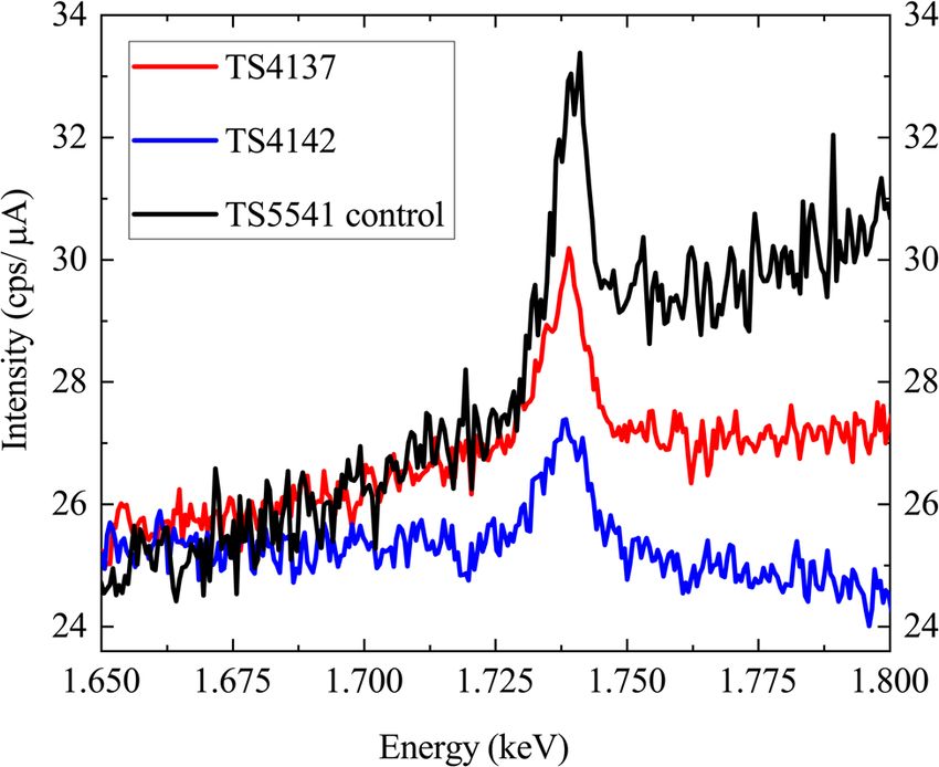
Microscopy and Microanalysis                                                                                                                                                 697

        electron beam-induced current (EBIC; Wallace et al., 2014), and
        electron channeling contrast imaging (ECCI) signals
        (Naresh-Kumar et al., 2020). Some limitations of the WDX tech-
        nique are that depth resolution is a function of the electron acceler-
        ating voltage, which must be high enough to excite all the relevant
        X-ray lines, preferably with an overvoltage ratio of at least 2 to ensure
        accurate analysis, particularly when approaching detection limits.
        These limitations also introduce constraints on the minimum sam-
        ple thickness (Newbury, 2002) and depth profiling, where SIMS per-
        forms strongly including for nitride semiconductor structures
        (Martin et al., 2006; Wei et al., 2014; Michałowski et al., 2019;
        Pickrell et al., 2019). Two of these works employed time-of-flight
        SIMS (TOF-SIMS) which has a number of advantages over
        D-SIMS, including dual-source depth profiling where the two ion
        beams have been optimized for their respective tasks, although
        work is needed to achieve the same detection limit for dopants
        (Klump et al., 2018).                                                                      Fig. 1. SIMS profiles for Si and Al for a sample for which there was an interruption
            The capability of the WDX technique for measuring dopants                              during the MOCVD growth. The sample consists of InAlGaN on top of a thick AlGaN:Si
        within semiconductor epilayers has been reported by Deatcher                               layer grown in two parts, with a change of reactors at a depth of approximately 500 nm.

        et al. (2006) and Kusch et al. (2017). The latter compared
        WDX data for Si concentration ranges 40–350 ppm (3 × 10¹⁸–
                                                                                                   surface, and it should be noted that the graphite susceptors
        2.8 × 1019 cm−3) in AlxGa1–xN with commercially performed
                                                                                                   used to heat and support the substrate wafer during growth are
        D-SIMS on some of the samples in the study. Both measurement
                                                                                                   often coated with SiC to provide robustness. It typically takes
        methods showed the same general trend: a linear increase in the Si
                                                                                                   about 30 min for the samples to cool down from the growth tem-
        concentration with increasing SiH4/III (silane to group-III ratio),
                                                                                                   perature and possible sources of Si contamination during that
        but the Si concentration measured by WDX was higher by a factor
                                                                                                   period include the reactor walls, precursors, substrates, or quartz
        of approximately 2 compared with D-SIMS. The reason for the
                                                                                                   liners (as molten Ga can etch the quartz to produce gallium oxide
        discrepancy between the different types of measurement was
                                                                                                   and free silicon). It is possible that there is a constant background
        not clarified at the time (Kusch et al., 2017). However, the reports
                                                                                                   source of Si within the reactor and the incorporation of Si has
        in Deatcher et al. (2006) and Robin et al. (2016) show that it is
                                                                                                   been shown to increase sharply when the ammonia flow drops
        possible to use X-ray microanalysis to measure doping levels in
                                                                                                   (Koleske et al., 2002). After removing a sample from the growth
        semiconductor epilayers, with Robin et al. using EDX to address
                                                                                                   chamber, silicate dust in the air and silicone oils are a likely source
        quantitation of dopants. The report of Deatcher et al. (2006)
                                                                                                   of Si contamination of the surfaces. SIMS data for samples where
        shows that Mg measurement in GaN gives very good agreement
                                                                                                   there has been a growth interruption to allow transfer between
        between WDX and D-SIMS. The question of why WDX measure-
                                                                                                   reactors reveal contamination with Si. This is illustrated in
        ment appears to over-estimate values for the Si doping is the sub-
                                                                                                   Figure 1 for an AlGaN:Si layer grown in two stages. The spike
        ject of this investigation. Donovan et al. (2011) developed
                                                                                                   in the Si trace at a depth of approximately 500 nm shows a signif-
        optimum measurement practices for WDX trace analysis which
                                                                                                   icant increase in its concentration at the interruption interface.
        we will apply in the analysis of Si doping.
                                                                                                   Such a spike has also been observed in samples where there is
            Over the years, many research groups have addressed the
                                                                                                   no Si doping as well as ones where there was simply a pause in
        trace-element capabilities of the WDX technique. Some early
                                                                                                   epitaxy, with no change in the reactor, to allow changes in growth
        examples include the analysis of Ge distribution in iron meteor-
                                                                                                   parameters such as temperature and pressure. SIMS profiles from
        ites (Goldstein, 1967), transition elements in ferromagnesian sili-
                                                                                                   Pickrell et al. (2019) reveal significantly greater Si concentration in
        cate minerals (Merlet & Bodinier, 1990), trace elements in
                                                                                                   GaN due to air contamination when compared with growth inter-
        minerals (McKay & Seymour, 1982), and trace elements in glass
                                                                                                   ruptions with temperature ramps. In both cases, the oxygen trace
        (Fialin et al., 1999). More recent works focus on specific situations
                                                                                                   remained at the detection limit.
        or on refinements of the technique and conditions for trace anal-
                                                                                                       Furthermore, a number of groups fabricating GaN-based
        ysis, such as the works from Allaz et al. (2019), Batanova et al.
                                                                                                   nanowires have discussed Si-rich layers forming on the surface
        (2018), Buse et al. (2018), Carpenter et al. (2002), Donovan
                                                                                                   of nanowires grown with high silane flows and which impact
        et al. (2011, 2016), Fournelle (2007), von der Handt et al.
                                                                                                   the lateral-to-vertical growth rates (Tessarek et al., 2014; Ren
        (2016), Jercinovic et al. (2005, 2012), Reed (2000, 2002), Sato
                                                                                                   et al., 2018). These layers are clearly visible in EDX maps obtained
        et al. (2007), and Zhang et al. (2016).
                                                                                                   using transmission electron microscopy and although only a few
            In this paper, we will consider how to measure Si, at dopant
                                                                                                   nm thick contain high concentrations of Si.
        levels, in semiconductor epilayers such as GaN and AlxGa1–xN
        where inherent contamination of the sample surfaces with addi-
        tional Si is suspected to be the cause of a discrepancy between
                                                                                                   Materials and Methods
        the results from D-SIMS and WDX. Si incorporation is known
        to be a contaminant during the metal-organic chemical vapor                                The aim of this study was to explore the use of WDX in a com-
        deposition (MOCVD) growth of GaN and AlxGa1–xN (Koleske                                    mercial EPMA (JEOL JXA-8530F) to simultaneously measure the
        et al., 2002; Pickrell et al., 2019). Typical growth temperatures                          concentration of major (alloy) and minor (dopant) elements
        are in the region of 1,100°C, in order to promote the breakup                              within semiconductor epilayers at specific points on the sample
        of the ammonia molecules and adatom mobility on the growing                                surface. We demonstrate a new approach to correct for the

Downloaded from https://www.cambridge.org/core. IP address: 81.105.13.203, on 06 Aug 2021 at 12:27:24, subject to the Cambridge Core terms of use, available at
https://www.cambridge.org/core/terms. https://doi.org/10.1017/S1431927621000568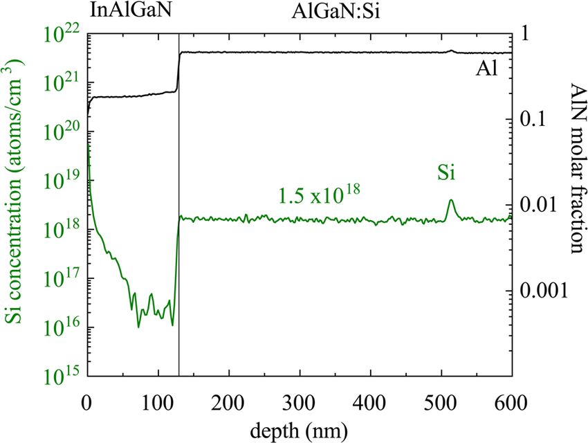
698                                                                                                                                                 Lucia Spasevski et al.

       Table 1. Reference GaN and AlxGa1–xN Samples for Which Independent Measurement of the Si Concentration Is Available.

                                                    Si net (Peak                                                                                    WDX concentration
                                      AlN           intensity-background                    WDX concentration           SIMS concentration          (×1018 cm−3) from the
           Sample name                at.%          intensity) (cps/μA)                     (×1018 cm−3)                (×1018 cm−3)                University of Bristol EPMA lab

           TS4142 (GaN)               0             188 ± 16                                6.2 ± 0.6 (coated)          0.743                       10.0 ± 2.0
                                                                                            6.5 ± 0.7 (uncoated)
           TS4137 (GaN)               0             208 ± 19                                6.3 ± 0.4 (coated)          0.212                       20.0 ± 0.9
                                                                                            10 ± 2 (uncoated)
           TS5541 (“blank”            76a           192 ± 44                                7.0 ± 2.0                   0a                          –
           AlxGa1–xN), control
           sample
           TS2039 (AlxGa1–xN)         94 ±          220 ± 22                                9.0 ± 0.3                   3.6 ± 0.7                   7.0 ± 0.6
                                      3b
           TS1860 (AlxGa1–xN)         80 ±          306 ± 27                                9.0 ± 0.4                   4.1 ± 0.8                   10.0 ± 2.0
                                      3bc
                                                                                                                        7.0 ± 4.0
           EU2000894 (GaN)            0c            857 ± 44                                40.0 ± 3.0                  12.0 ± 0.6                  –
                                                                                                                        13
           TS5565 (AlxGa1–xN)         57            634 ± 5                                 21.4 ± 0.5                  8.3                         –
                                                                                            (uncoated)
           TS5587 (AlxGa1–xN)         62            1,062 ± 15                              27.3 ± 2.0                  13.4                        –
                                                                                            (uncoated)
           TS5712 (AlxGa1–xN)         79            506 ± 10                                14.8 ± 0.5                  4.0                         –
                                                                                            (uncoated)
           TS5770 (AlxGa1–xN)         80            260 ± 11                                7.6 ± 0.9 (uncoated)        1.4                         –
           TS5602 (AlxGa1–xN)         60            1,700 ± 36                              37.1 ± 3.7                  20.8                        –
                                                                                            (uncoated)
       a
        Sample TS5541 has not been measured by SIMS, but it was grown undoped, so the SIMS concentration is assigned to be 0; AlN at.% as estimated from the growth conditions.
       b
        From Kusch et al. (2017).
       c
        Samples TS1860 and EU2000894 were measured by two of the three SIMS companies.

       overestimation in measured Si donor concentration caused by                                    D-SIMS data were provided by three different companies: RTG
       inherent contamination of the sample surfaces with additional Si.                          Mikroanalyse GmbH Berlin (Jörchel et al., 2016), Loughborough
           A range of Si-doped GaN and AlxGa1–xN samples, grown by                                Surface Analysis Ltd. (using a Cameca 7f), and Evans Analytical
       MOCVD by different groups, were used to clarify the best way                               Group (EAG). All samples were analyzed in a depth profile mode,
       to measure Si. GaN:Si material (sample EU2000894) was provided                             using areas typically 100 × 100 μm. RTG used ion-implanted
       by IQE Europe Ltd. A series of AlxGa1–xN samples with different                            AlGaN samples to produce absolute and relative sensitivity factors
       crystal polarities and different AlN contents was provided by                              for Si in AlGaN, with further details given in Jörchel et al. (2016).
       the Tyndall Institute. These AlxGa1-xN samples included polar-                             The same approach was used for data from Loughborough. EAG
       oriented [0001] (samples AP, BP, CP) and semipolar-oriented lay-                           used a proprietary method that calculates the change in sensitivity
       ers [112-2] (samples ASP, CSP). More details on the growth of the                          factors with respect to the AlN fraction in AlGaN.
       AlxGa1–xN:Si layers from the Tyndall Institute are given elsewhere                             WDX measurements were performed in the EPMA with the inci-
       (Li et al., 2013; Dinh et al., 2016a, 2016b; Pampili et al., 2018;                         dent electron beam normal to the sample surface, and an accelera-
       Spasevski et al., 2021). Samples labeled TS are AlxGa1–xN layers                           tion voltage of 10 kV which is sufficient to efficiently excite the
       with various AlN contents and crystal polarities grown at                                  selected X-ray lines. Under these conditions, the electron interaction
       Technische Universität Berlin (Knauer et al., 2013; Kusch et al.,                          volume is kept within the first 500–800 nm of the AlxGa1–xN layer
       2014; Mehnke et al., 2016; Foronda et al., 2020). The “blank”                              according to Monte Carlo simulations using CASINO software
       AlxGa1–xN TS5541 was grown with no Si doping and quickly                                   (Drouin et al., 2007) and dependent on the AlN molar content. In
       shipped in a sealed container filled with N2 gas in order to min-                          all samples, the interaction volume is contained within the top
       imize contamination and on receipt it was immediately placed                               most AlxGa1–xN layer. The beam current was 40 nA for analysis
       under vacuum within the EPMA chamber. Information on the                                   of the major elements (Al, Ga, N) and increased to 400–500 nA
       three sets of samples is given in Tables 1 and 2. Attempts were                            for the minor elements. The beam was defocussed to 10 or 20 μm
       made to remove inherent surface contamination by oxygen                                    to improve sample averaging and avoid damaging the sample. The
       plasma cleaning treatments. Traditionally, plasma cleaning is                              samples and standards were carbon coated to remove charging
       employed to remove hydrocarbon contamination (Donovan &                                    effects, with a thickness of approximately 15 nm [as determined
       Rowe, 2005). Apart from contamination, the samples can also suf-                           by the interference-color method of Kerrick et al. (1973)]. This
       fer from oxidation. To investigate the effect of oxidation of the Si                       becomes increasingly important for AlN-rich AlxGa1–xN for which
       standard, cleaning with HF solution was employed.                                          the conductivity decreases. Measurements were also performed on

Downloaded from https://www.cambridge.org/core. IP address: 81.105.13.203, on 06 Aug 2021 at 12:27:24, subject to the Cambridge Core terms of use, available at
https://www.cambridge.org/core/terms. https://doi.org/10.1017/S1431927621000568
Microscopy and Microanalysis                                                                                                                                           699

        Table 2. List of AlxGa1–xN Samples for Which Independent Constraint on the Composition Is Not Available, Measured AlN at.% Using WDX and Si Kα Intensity Values
        Together with the Calculated Si Concentration (Crystal Orientation [0001] AxP, Orientation [1122] AxSP).

                                                                  Calculated ZAF factor               Calculated Si concentration               Calculated Si concentration (ppm)
           Sample            WDX AlN           WDX Si net            for the Si Kα in              (1018 cm−3) using the calibration            using the calibration method and
           name               at.%              (cps/μA)                AlxGa1–xN                   method and calcZAF software                 calcZAF software

           A1SP              56.6 ± 0.6          175 ± 16                  1.283                                   3.1                          31
           A2SP              65.5 ± 0.7          440 ± 13                  1.289                                   5.7                          61
           A3SP              61.2 ± 0.7          469 ± 54                  1.286                                   6.2                          65
           A4SP              59.4 ± 0.7          463 ± 19                  1.285                                   6.2                          64
           A5SP              59.6 ± 0.7          374 ± 10                  1.285                                   5.2                          54
           A1P               63.0 ± 0.7          218 ± 33                  1.287                                   3.4                          36
           A2P               71.7 ± 0.8          253 ± 22                  1.294                                   3.5                          40
           A3P               68.8 ± 0.7          320 ± 6                   1.292                                   4.3                          47
           A4P               62.7 ± 0.7          534 ± 9                   1.287                                   6.8                          72
           A5P               69.3 ± 0.7          743 ± 9                   1.292                                   8.6                          96

        two of the GaN:Si sample without coatings (and using uncoated                              concentrations necessitate a separate measurement routine to
        standards) to confirm that the coating was not a source of Si.                             that for the major elements, due to different requirements for
            According to best practice for trace analysis, the pulse height                        the counting statistics between the major and minor elements
        analysis (PHA) parameters (such as voltage window, baseline,                               (Sato et al., 2007). Therefore, to improve counting statistics, lon-
        electronic bias, and gain on the detector) were adjusted before                            ger measurement times and higher currents were employed: 400–
        measuring the Si Kα peak, using counter energy distributions of                            500 nA, and 360 and 180 s counting times for the peak and back-
        the peak on a pure Si standard with a beam current of 20 nA                                ground, respectively. The accelerating voltage and measurement
        (Reed, 2002). Si has the tendency for a peak shift due to valence                          positions were kept unchanged in order to ensure that the data
        and coordination (Fournelle, 2006), but in our case, the shifts in                         for the silicon and major elements will refer to the same volumes
        the Si Kα peak position between pure Si standard and the                                   within the sample. Unlike an EDX detector, WDX spectrometers
        unknown samples were insignificant. The differential mode was                              record only one wavelength at a time so there is no risk of over-
        employed simply to exclude noise peaks and no higher-order                                 saturating the detector with major element counts when measur-
        interferences were observed in the region of the Si Kα peak                                ing silicon with high current. With the new measurement
        (Geller & Herrington, 2002; Zhang et al., 2016).                                           condition, the counting statistics were significantly improved for
            In this paper, two methods were employed for checking the                              silicon and the counting error was reduced to 1–3% relative,
        presence of Si dopants: qualitative and quantitative measurement.                          with detection limit (DL) reduced to 1 ppm. Despite the smaller
        In the qualitative scan, the information on the element concentra-                         errors in the silicon signal, the final silicon concentration in the
        tion is present in the height of the peak, extracted as peak maxi-                         sample still resulted in higher concentrations [(0.6–4) ×
        mum minus interpolated background. For the quantitative                                    1019 cm−3 levels] than expected when compared with SIMS data
        measurements, the EPMA’s standard ZAF correction procedure                                 available for the same samples.
        was used in the usual way to determine the Si concentration                                    In order to check the accuracy of measured results, an inter-
        and the results are included in Table 1. The quantitative proce-                           laboratory study was conducted and some samples were also mea-
        dure improves counting statistics due to the extended time                                 sured on the EPMA (JEOL JXA-8530F) at the University of
        spent acquiring peak and background X-rays, compared with                                  Bristol.
        the qualitative scan. The concentration of the major elements is
        quantified using the ratios of the background-corrected peak
        intensities for the sample to the corresponding ones obtained                              Results and Discussion
        from AlN, GaN, and Si standards (k-ratios). Signals were acquired                          In order to test the detection limit of approximately 10 ppm (1σ),
        for 60 s on the peak positions and for 30 s on the background                              which corresponds to concentrations of 1018 cm−3 of Si in GaN,
        positions with a beam current of 20 nA. Ga Lα and Al Kα signals                            we performed WDX measurements on two GaN: Si samples
        were recorded using a TAPH crystal (thallium acid phthalate,                               (TS4142 and TS4137) with low silicon contents that were also
        100 mm Rowland circle), while for the N Kα signal, a synthetic                             characterized by SIMS (Table 1), and on one “blank” AlxGa1–xN
        layered LDE1L crystal (140 mm Rowland circle) was used. For                                sample TS5541. Figure 2 shows long qualitative WDX scans
        quantification of the minor element, the Si Kα X-rays were                                 (dwell time 12 s, 505 points, total time: 1 h 36 min), which were
        recorded using a large TAP crystal (140 mm Rowland circle).                                performed to check for the existence of the Si Kα peak. A Si
        The measured intensities are corrected for differences in compo-                           peak is clearly visible above the background level in all of the
        sition between standard and specimen using the standard ZAF                                above-mentioned samples (even in the “blank” sample, referred
        correction procedures in the JEOL EPMA software. The ZAF                                   from now on as a control sample) and much greater than error/
        method consists of corrections for atomic number                                           detection limit. We conclude that sample TS5541 is not actually
        (Philibert-Tixier method), absorption (Philibert method), and                              blank and has accrued Si either during growth or in the time
        fluorescent excitation (Reed method). The low silicon                                      before measurement. From the qualitative scans, it is also possible

Downloaded from https://www.cambridge.org/core. IP address: 81.105.13.203, on 06 Aug 2021 at 12:27:24, subject to the Cambridge Core terms of use, available at
https://www.cambridge.org/core/terms. https://doi.org/10.1017/S1431927621000568
700 Lucia Spasevski et al.
Table 3. Si Kα Intensities Acquired for Pure Si Standard, Before and After
Removal of Native Oxide Layer.
Before After
TAPL crystal, cleaning cleaning Percentage
20 nA, 10 kV (counts) (counts) difference (%)
Uncoated 76,313 79,353 4
Coated 78,596 80,823 3
in the intensity of Si Kα peak. We can assume that the native oxy-
gen layer was thinner than 10 nm (Carpenter, 2008).
Thus, as far as we can tell, cleaning treatments did not remove
possible Si contamination and that oxidation of the sample or
standard is not the reason for the large discrepancy between
SIMS and WDX results. The data measured from two GaN:Si
samples, with and without C-coating, confirm that the C-coat is
not the source of extra Si.
Fig. 2. Long qualitative scan (dwell time 12 s) for the Si Kα peak from GaN:Si samples: After cleaning the Si standard, calibration data was acquired
TS4142 (blue), TS4137 (red), and AlxGa1–xN control sample TS5541 (black) using a from it using a very low current of 1 nA in order to reduce the
TAPL crystal at 10 kV, 400 nA (100 nA for the control sample). count difference between the standard and unknown trace element.
This did not result in any difference in the measured concentration
for the trace element when compared with calibration data acquired
to conclude that there are no signs of any interference close to the with 20 nA. Subsequently, all calibration data are acquired with a
Si Kα peak that could be a serious source of error in quantitative lower beam current of 20 nA compared with the 500 nA employed
microanalysis and that the peak position is the same in the tested to measure Si in the unknowns, in order to avoid detector oversat-
samples (Donovan et al., 1993). There are differences in the shape uration. In doing this, we have relied on the current measurement
of the background for the samples shown in Figure 2, with the system scaling linearly from 20 to 500 nA.
main difference being the high Al content in TS5541 which Due to the long measurement time and high currents used for
could be responsible for the increased background on the high- the silicon analysis, the instrumental and sample stability need to
energy side for this sample. be checked (Hughes et al., 2019). A sample will generally be stable
Since the SIMS measurements (for the GaN samples) gave values during analysis with usual operating conditions (10–100 nA), but
below or close to the detection limit, the silicon doping should have the high currents (hundreds of nA) required for trace-element
been unmeasurable in these cases. However, the WDX data show analysis may cause it to degrade (Carpenter et al., 2002). It is nec-
clear Si X-ray peaks and high apparent Si content (>6 × 1018 cm−3 essary to assess if the samples are stable during measurement time
compared withMicroscopy and Microanalysis 701
Fig. 3. Time scan for Si Kα in the GaN:Si calibration sample under “trace analysis”
Fig. 5. Plot of the calculated matrix correction (ZAF correction) from elemental Si
electron-beam operating conditions showing a constant Si Kα count rate and against AlN at.% as measured by WDX for each of the AlxGa1–xN samples.
absorbed current as a function of time, showing only minor change in the absorbed
current during long counting times.
Fig. 6. Calibration relation with all the points representing Si intensity in GaN (For the
Fig. 4. Correlation between Si intensity measured by WDX and the concentration
AlxGa1–xN points, the Si concentration from D-SIMS is converted to its equivalent for
from SIMS data for GaN (red points) and AlxGa1–xN (black points) samples.
GaN using calcZAF software). The orange dotted line represents the Si sensitivity level
for GaN.
The change in matrix correction (ZAF correction) for Si for
different AlN contents was estimated using the stand-alone enables the Si concentration in AlxGa1–xN samples of any compo-
CalcZAF software (Donovan et al., 2019), as plotted in Figure 5. sition to be estimated by measuring the Si intensity. For samples
The different correction procedures available in CalcZAF software with Si net ≤200 cps/μA (e.g. sample A1SP), the equivalent Si
did not produce a noticeable difference in the correction factors. concentration is set to the sensitivity limit of 35 ppm, which cor-
The calculated ZAF parameters are then used to adjust all the responds to concentrations ranging from 2.4 × 1018 cm−3 for AlN
D-SIMS calibration points to the effective value for a GaN host, as or 4.6 × 1018 cm−3 for GaN, calculated from the calibration curve
shown in Figure 6. This resulting calibration relation allows the Si in Figure 6.
content to be estimated in samples of all AlxGa1–xN compositions Figure 8 plots the calculated Si concentrations against the dis-
by measuring the Si intensity, then using the GaN calibration ilane to group III ratios (Si2H6/III ratios) (Dinh et al., 2016a,
curve with the appropriate ZAF correction. 2016b; Pampili et al., 2018). In MOCVD growth, the group III
This process is illustrated using the series of AlxGa1–xN sam- atoms are introduced via metal precursors in the form of organic
ples listed in Table 2. The measured intensity values, Si net compounds such as trimethylgallium and trimethylaluminium,
(cps/μA), are adjusted to the effective Si net values for GaN, while ammonia is the nitrogen source. Doping can be obtained
using the ZAF correction procedure, and these are then converted by introducing into the reactor dopant-containing gases, such
to Si concentration using the calibration curve. The calculated Si as disilane (Si2H6) (Pampili & Parbrook, 2017). The measured
concentrations in AlxGa1–xN are plotted in Figure 7, which also Si concentrations for the semipolar ASP samples increase linearly
shows the calibration line for GaN for comparison. This method with the Si2H6/III ratio up to a saturation point of 2.3 × 10⁻⁴
Downloaded from https://www.cambridge.org/core. IP address: 81.105.13.203, on 06 Aug 2021 at 12:27:24, subject to the Cambridge Core terms of use, available at
https://www.cambridge.org/core/terms. https://doi.org/10.1017/S1431927621000568702 Lucia Spasevski et al.
xN layers with varying AlN contents and polarity. The highest val-
ues of Si incorporation were observed for polar samples
(100 ppm), while saturation of Si incorporation was seen for semi-
polar samples at a high Si/III ratio. The advantages of the WDX
approach include high lateral spatial resolution and the ability to
determine the alloy composition of the major elements, such as
Al, Ga, and N, at the same time as the doping levels. The stan-
dards used in WDX analysis are more accessible compared with
ion-implanted standards required for the SIMS analysis. Apart
from the quantitative abilities of the EPMA instrument, another
major advantage in the examination of the semiconductor alloys
is the correlation of WDX data with other microscopy techniques
such as CL and ECCI as well as the high-resolution mapping
capabilities.
Acknowledgments. The authors thank Dr. Trevor Martin from IQE Europe
Ltd., for providing additional GaN:Si samples, and to Drs. Vitaly Zubialevich,
Pietro Pampili, and Duc Dinh from Tyndall National Institute for providing
Fig. 7. Values for Si concentration in AlxGa1–xN:Si layers plotted against the measured additional AlGaN:Si samples. We acknowledge Alison Chew of
Si net signal. The line is the calculated calibration for GaN:Si and the points differ Loughborough Surface Analysis Ltd. for provision of D-SIMS measurement
from this line according to the amount of AlN contained in the host material. and discussion of the results. We thank Dr. Gunnar Kusch for useful discus-
sion and advice. We thank Dr. Stacey Laing from the Department of Pure and
Applied Chemistry, University of Strathclyde, for performing plasma cleaning of
the samples. We would also like to show our gratitude to Mr. James Sweeney and
Dr. Ian Watson from the Institute of Photonics, University of Strathclyde, for
cleaning the samples with HF solution. This work was supported by the
EPSRC project EP/N010914/1, “Nanoanalysis for Advanced Materials and
Healthcare,” by the EU-FP7 programme “ALIGHT,” Science Foundation
Ireland through SFI/10/IN.1/I2993 and Irish Photonic Integration Centre (SFI/
12/RC/2276_2), and the European Space Agency. All data underpinning this pub-
lication are openly available from the University of Strathclyde KnowledgeBase at:
https://doi.org/10.15129/aa61c668-99ca-4802-9013-ff5f15409240.
References
Allaz JM, Razvan-Gabriel P, Reusser E & Martin L (2019). Electron micro-
probe analysis of minor and trace elements in beam sensitive materials:
How far can we go? Microsc Microanal 25(S2), 2312–2313.
Amano H, Collazo R, Santi CD, Einfeldt S, Funato M, Glaab J, Hagedorn S,
Hirano A, Hirayama H, Ishii R, Kashima Y, Kawakami Y, Kirste R,
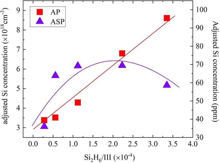
Fig. 8. Si concentration of the AlxGa1–xN-doped layer as a function of disilane to Kneissl M, Martin R, Mehnke F, Meneghini M, Ougazzaden A,
group III ratio, as evaluated by WDX. The solid lines provide guides to the eye. Parbrook PJ, Rajan S, Reddy P, Römer F, Ruschel J, Sarkar B, Scholz
F, Schowalter LJ, Shields P, Sitar Z, Sulmoni L, Wang T, Wernicke T,
Weyers M, Witzigmann B, Wu Y-R, Wunderer T & Zhang Y (2020).
Si2H6/III. The saturation point is consistent with a previous report The 2020 UV emitter roadmap. J Phys D: Appl Phys 53(50), 503001.
from Dinh et al. (2016a), where the carrier concentration and Batanova VG, Sobolev AV & Magnin V (2018). Trace element analysis by
mobility of semipolar layers were observed to reach a maximum EPMA in geosciences: Detection limit, precision and accuracy. IOP Conf
at a similar Si2H6/III ratio. The AP series exhibits an almost linear Ser: Mater Sci Eng 304, 012001.
Buse B, Wade J, Llovet X, Kearns S & Donovan JJ (2018). Secondary fluo-
increase of Si with disilane flow rate.
rescence in WDS: The role of spectrometer positioning. Microsc
Microanal 24(6), 604–611.
Summary Carpenter P, Counce D, Kluk E & Nabelek C (2002). Characterization of
corning EPMA standard glasses 95IRV, 95IRW, and 95IRX. J Res Natl
The use of WDX spectroscopy for the measurement of silicon- Inst Stand Technol 107(6), 703–718.
doping levels in wide band-gap AlxGa1–xN layers is demonstrated Carpenter PK (2008). EPMA standards: The good, the bad, and the ugly.
in a commercially available EPMA instrument. A previously Microsc Microanal 14(S2), 530–531.
reported limitation with over-estimates of the Si contents was Deatcher C, Bejtka K, Martin R, Romani S, Kheyrandish H, Smith L,
thoroughly investigated and was assigned to surface contamina- Rushworth S, Liu C, Cheong M & Watson I (2006).
Wavelength-dispersive X-ray microanalysis as a novel method for studying
tion. An analytical routine was introduced for measuring the
magnesium doping in gallium nitride epitaxial films. Semicond Sci Technol
trace Si levels, consisting of separate measurement of Si with
21, 1287–1295.
high current and long counting times followed by calibration Dinh DV, Alam SN & Parbrook PJ (2016a). Effect of V/III ratio on the
using D-SIMS measurements. By measuring silicon intensities growth of ([1122]) AlGaN by metalorganic vapour phase epitaxy. J Cryst
and using a calibration curve fit method using the D-SIMS data Growth 435, 12–18.
along with calculated ZAF correction values, it was possible to Dinh DV, Pampili P & Parbrook PJ (2016b). Silicon doping of semipolar
determine doping levels of order (3–10) × 1018 cm−3 in AlxGa1– ([1122])AlxGa1−xN(0.50≤x≤0.55). J Cryst Growth 451, 181–187.
Downloaded from https://www.cambridge.org/core. IP address: 81.105.13.203, on 06 Aug 2021 at 12:27:24, subject to the Cambridge Core terms of use, available at
https://www.cambridge.org/core/terms. https://doi.org/10.1017/S1431927621000568Microscopy and Microanalysis 703
Donovan J, Pinard P & Demers H (2019). High speed matrix corrections for Kusch G, Mehnke F, Enslin J, Edwards PR, Wernicke T, Kneissl M &
quantitative X-ray microanalysis based on Monte Carlo simulated K-ratio Martin RW (2017). Analysis of doping concentration and composition in
intensities. Microsc Microanal 25(3), 735–742. wide bandgap AlGaN:Si by wavelength dispersive X-ray spectroscopy.
Donovan J & Rowe M (2005). Techniques for improving quantitative analysis Semicond Sci Technol 32(3), 7.
of mineral glasses. Geochim Cosmochim Acta 69(Suppl 10), 589. Lee MR, Martin RW, Trager-Cowan C & Edwards PR (2005). Imaging of
Donovan JJ, Lowers HA & Rusk BG (2011). Improved electron probe micro- cathodoluminescence zoning in calcite by scanning electron microscopy
analysis of trace elements in quartz. Am Mineral 96(2–3), 274–282. and hyperspectral mapping. J Sediment Res 75(2), 313–322.
Donovan JJ, Singer JW & Armstrong JT (2016). A new EPMA method for fast Li H, Sadler TC & Parbrook PJ (2013). Aln heteroepitaxy on sapphire by met-
trace element analysis in simple matrices. Am Mineral 101(8), 1839–1853. alorganic vapour phase epitaxy using low temperature nucleation layers. J
Donovan JJ, Snyder DA & Rivers ML (1993). An improved interference cor- Cryst Growth 383, 72–78.
rection for trace element analysis. Microbeam Anal 2, 23–28. Martin RW, Edwards PR, O’Donnell KP, Dawson MD, Jeon C-W, Liu C,
Drouin D, Couture AR, Dany J, Tastet X, Aimez V & Gauvin R (2007). Rice GR & Watson IM (2004). Cathodoluminescence spectral mapping
CASINO v2.42—A fast and easy-to-use modeling tool for scanning electron of III-nitride structures. Phys Status Solidi (A) 201(4), 665–672.
microscopy and microanalysis users. Scanning 29(3), 92–101. Martin RW, Rading D, Kersting R, Tallarek E, Nogales E, Amabile D,
Edwards PR, Jagadamma LK, Bruckbauer J, Liu C, Shields P, Allsopp D, Wang Wang K, Katchkanov V, Trager-Cowan C, O’Donnell KP, Watson IM,
T & Martin RW (2012). High-resolution cathodoluminescence hyperspectral Matias V, Vantomme A, Lorenz K & Alves E (2006). Depth profiling of
imaging of nitride nanostructures. Microsc Microanal 18(6), 1212–1219. ion-implanted AlInN using time-of-flight secondary ion mass spectrometry
Edwards PR & Martin RW (2011). Cathodoluminescence nano- and cathodoluminescence. Phys Status Solidi C 3(6), 1927–1930.
characterization of semiconductors. Semicond Sci Technol 26(6), 064005. McKay G & Seymour R (1982). Electron microprobe analysis of trace ele-
Fialin M, Remy H, Richard C & Wagner C (1999). Trace element analysis ments in minerals at 10 PPM concentrations. Proceedings, Annual
with the electron microprobe: New data and perspectives. Am Mineral 84 Conference - Microbeam Analysis Society.
(1–2), 70–77. Mehnke F, Trinh XT, Pingel H, Wernicke T, Janzén E, Son NT & Kneissl M
Foronda HM, Hunter DA, Pietsch M, Sulmoni L, Muhin A, Graupeter S, (2016). Electronic properties of Si-doped AlxGa1−xN with aluminum mole
Susilo N, Schilling M, Enslin J, Irmscher K, Martin RW, Wernicke T fractions above 80%. J Appl Phys 120(14), 145702.
& Kneissl M (2020). Electrical properties of (11-22) Si:AlGaN layers at Merlet C & Bodinier J-L (1990). Electron microprobe determination of minor and
high Al contents grown by metal-organic vapor phase epitaxy. Appl Phys trace transition elements in silicate minerals: A method and its application to
Lett 117(22), 221101. mineral zoning in the peridotite nodule PHN 1611. Chem Geol 83(1), 55–69.
Fournelle J (2006). Silicate peak shifts, spectrometer peaking issues and stan- Merlet C & Llovet X (2012). Uncertainty and capability of quantitative EPMA
dard/specimen size discrepancies in EPMA: 3 Bumps in the road to the goal at low voltage – A review. IOP Conf Ser: Mater Sci Eng 32, 012016.
of 1% accuracy. In AGU Spring Meeting Abstracts. Michałowski PP, Złotnik S & Rudziński M (2019). Three dimensional local-
Fournelle J (2007). Problems in trace element EPMA: Modeling secondary ization of unintentional oxygen impurities in gallium nitride. Chem
fluorescence with PENEPMA. In AGU Fall Meeting Abstracts, pp. Commun 55(77), 11539–11542.
V51A-0329. Naresh-Kumar G, Alasmari A, Kusch G, Edwards PR, Martin RW, Mingard
Geller JD & Herrington C (2002). High count rate electron probe microanal- KP & Trager-Cowan C (2020). Metrology of crystal defects through inten-
ysis. J Res Natl Inst Stand Technol 107(6), 503–508. sity variations in secondary electrons from the diffraction of primary elec-
Goldstein JI (1967). Distribution of germanium in the metallic phases of some trons in a scanning electron microscope. Ultramicroscopy 213, 112977.
iron meteorites. J Geophys Res (1896–1977) 72(18), 4689–4696. Newbury DE (2002). Barriers to quantitative electron microanalysis for low
Hughes EC, Buse B, Kearns SL, Blundy JD, Kilgour G & Mader HM (2019). voltage electron microscopy. J Res Natl Inst Stand Technol 107(6), 605–619.
Low analytical totals in EPMA of hydrous silicate glass due to sub-surface Pampili P, Dinh DV, Zubialevich VZ & Parbrook PJ (2018). Significant con-
charging: Obtaining accurate volatiles by difference. Chem Geol 505, 48–56. tribution from impurity-band transport to the room temperature conduc-
Jercinovic M, Williams M, Allaz J & Donovan J (2012). Trace analysis in tivity of silicon-doped AlGaN. J Phys D: Appl Phys 51(6), 06LT01.
EPMA. IOP Conf Ser: Mat Sci Eng 32. Pampili P & Parbrook PJ (2017). Doping of III-nitride materials. Mater Sci
Jercinovic MJ & Williams ML (2005). Analytical perils (and progress) in elec- Semicond Process 62, 180–191.
tron microprobe trace element analysis applied to geochronology: Pickrell GW, Armstrong AM, Allerman AA, Crawford MH, Cross KC,
Background acquisition, interferences, and beam irradiation effects. Am Glaser CE & Abate VM (2019). Regrown vertical GaN p–n diodes with
Mineral 90(4), 526–546. low reverse leakage current. J Electron Mater 48(5), 3311–3316.
Jercinovic MJ & Williams ML (2005). Analytical perils (and progress) in elec- Reed SJB (2000). Quantitative trace analysis by wavelength-dispersive EPMA.
tron microprobe trace element analysis applied to geochronology: Microchim Acta 132(2), 145–151.
Background acquisition, interferences, and beam irradiation effects. Am Reed SJB (2002). Optimization of wavelength dispersive X-ray spectrometry
Mineral 90(4), 526–546. analysis conditions. J Res Natl Inst Stand Technol 107(6), 497–502.
Jörchel P, Helm P, Brunner F, Thies A, Krüger O & Weyers M (2016). Ren CX, Tang F, Oliver RA & Zhu T (2018). Nanoscopic insights into the
Quantification of matrix and impurity elements in AlxGa1−xN compounds effect of silicon on core-shell InGaN/GaN nanorods: Luminescence, com-
by secondary ion mass spectrometry. J Vac Sci Technol B 34(3), 03H128. position, and structure. J Appl Phys 123(4), 045103.
Kerrick D, Eminhizer L & Villaume J (1973). The role of carbon film thick- Robin E, Mollard N, Guilloy K, Pauc N, Gentile P, Fang Z, Daudin B,
ness in electron microprobe analysis. Am Mineral 58, 920–925. Amichi L, Jouneau P, Bougerol C, Delalande M & Bavencove A (2016).
Klump A, Zhou C, Stevie FA, Collazo R & Sitar Z (2018). Improvement in Quantification of dopants in nanomaterial by SEM/EDS. European
detection limit for time-of-flight SIMS analysis of dopants in GaN struc- Microscopy Congress 2016: Proceedings.
tures. J Vac Sci Technol B 36(3), 03F102. Roccaforte F, Fiorenza P, Greco G, Lo Nigro R, Giannazzo F, Iucolano F &
Knauer A, Kueller V, Zeimer U, Weyers M, Reich C & Kneissl M (2013). Saggio M (2018). Emerging trends in wide band gap semiconductors (SiC
Algan layer structures for deep UV emitters on laterally overgrown AlN/ and GaN) technology for power devices. Microelectron Eng 187–188, 66–77.
sapphire templates. Phys Status Solidi (A) 210(3), 451–454. Sato A, Mori N, Takakura M & Notoya S (2007). Examination of analytical
Koleske DD, Wickenden AE, Henry RL & Twigg ME (2002). Influence of conditions for trace elements based on the detection limit of EPMA (WDS).
MOVPE growth conditions on carbon and silicon concentrations in GaN. JEOL News 42E (No.1).
J Cryst Growth 242(1), 55–69. Spasevski L, Kusch G, Pampili P, Zubialevich VZ, Dinh DV, Bruckbauer J,
Kusch G, Li H, Edwards PR, Bruckbauer J, Sadler TC, Parbrook PJ & Edwards PR, Parbrook PJ & Martin RW (2021). A systematic comparison
Martin RW (2014). Influence ofsubstrate miscut angle on surface morphol- of polar and semipolar Si-doped AlGaN alloys with high AlN content. J
ogy and luminescence properties of AlGaN. Appl Phys Lett 104(9), 092114. Phys D: Appl Phys 54(3), 035302.
Downloaded from https://www.cambridge.org/core. IP address: 81.105.13.203, on 06 Aug 2021 at 12:27:24, subject to the Cambridge Core terms of use, available at
https://www.cambridge.org/core/terms. https://doi.org/10.1017/S1431927621000568704 Lucia Spasevski et al.
Tessarek C, Heilmann M, Butzen E, Haab A, Hardtdegen H, Dieker C, von der Handt A, Allaz J & Neill OK (2016). Microanalytical standards,
Spiecker E & Christiansen S (2014). The role of Si during the growth of reference and research materials: Continuing the effort toward breaking
GaN micro- and nanorods. Cryst Growth Des 14(3), 1486–1492. the accuracy barrier. Microsc Microanal 22(S3), 424–425.
Tsao JY, Chowdhury S, Hollis MA, Jena D, Johnson NM, Jones KA, Kaplar RJ, Wallace MJ, Edwards PR, Kappers MJ, Hopkins MA, Oehler F, Sivaraya S,
Rajan S, Van de Walle CG, Bellotti E, Chua CL, Collazo R, Coltrin ME, Allsopp DWE, Oliver RA, Humphreys CJ & Martin RW (2014). Bias depen-
Cooper JA, Evans KR, Graham S, Grotjohn TA, Heller ER, dence and correlation of the cathodoluminescence and electron beam induced
Higashiwaki M, Islam MS, Juodawlkis PW, Khan MA, Koehler AD, current from an InGaN/GaN light emitting diode. J Appl Phys 116(3), 033105.
Leach JH, Mishra UK, Nemanich RJ, Pilawa-Podgurski RCN, Shealy Wei X, Zhao L, Wang J, Zeng Y & Li J (2014). Characterization of nitride-
JB, Sitar Z, Tadjer MJ, Witulski AF, Wraback M & Simmons JA based LED materials and devices using TOF-SIMS. Surf Interface Anal 46
(2018). Ultrawide-bandgap semiconductors: Research opportunities and (S1), 299–302.
challenges. Adv Electron Mater 4(1), 1600501. Zhang C, Koepke J, Wang L-X, Wolff P, Wilke S, Stechern A, Almeev R &
Van de Walle CG, Stampfl C, Neugebauer J, McCluskey MD & Johnson NM Holtz F (2016). A practical method for accurate measurement of trace level
(1999). Doping of AlGaN alloys. MRS Internet J Nitride Semicond Res 4(S1), fluorine in Mg- and Fe-bearing mineral and glass using electron probe
890–901. microanalysis. Geostand Geoanal Res 40, 351–363.
Downloaded from https://www.cambridge.org/core. IP address: 81.105.13.203, on 06 Aug 2021 at 12:27:24, subject to the Cambridge Core terms of use, available at
https://www.cambridge.org/core/terms. https://doi.org/10.1017/S1431927621000568You can also read