Programmable System on Chip for controlling an atomic physics experiment
←
→
Page content transcription
If your browser does not render page correctly, please read the page content below
Programmable System on Chip for controlling an atomic physics
                                                   experiment
                                                            A. Sitaram,1, a) G. K. Campbell,1 and A. Restelli1, b)
                                                            Joint Quantum Institute, University of Maryland and National Institute of Standards and Technology, College Park,
                                                            Maryland 20742, USA
                                                            (Dated: 14 April 2021)
                                                            Most atomic physics experiments are controlled by a digital pattern generator used to synchronize all equip-
                                                            ment by providing triggers and clocks. Recently, the availability of well-documented open-source development
                                                            tools has lifted the barriers to using programmable systems on chip (PSoC), making them a convenient and
                                                            versatile tool for synthesizing digital patterns. Here, we take advantage of these advancements in the design
                                                            of a versatile clock and pattern generator using a PSoC. We present our design with the intent of highlighting
arXiv:2102.11230v2 [physics.ins-det] 13 Apr 2021

                                                            the new possibilities that PSoCs have to offer in terms of flexibility. We provide a robust hardware carrier
                                                            and basic firmware implementation that can be expanded and modified for other uses.

                                                   I.   INTRODUCTION                                                 LabView, a systems engineering software that is com-
                                                                                                                     patible with National Instruments hardware, and AR-
                                                      Laser-cooled atoms, ions, and molecules are interest-          TIQ by M-labs18 , which is also a complete infrastruc-
                                                   ing and dynamic systems to study, and are being used              ture of software and hardware. Some university research
                                                   to develop many quantum technologies. These technolo-             groups have also created complete architectures, basing
                                                   gies include precise atomic clocks1,2 , quantum comput-           their hardware designs off of FPGAs and designing cus-
                                                   ers and simulators3,4 , and quantum sensors5,6 . Experi-          tom control software14,16 .
                                                   ments in atomic, molecular, and optical (AMO) physics                While FPGAs can work well as a primary control de-
                                                   are often a combination of a large number of commercial           vice for an experiment, microcontrollers offer a simpler
                                                   or custom-made instruments from different sources and             solution for handling complex communications protocols
                                                   manufacturers that need to operate synchronously and              such as USB (Universal Serial Bus) or Ethernet. Often, a
                                                   in a repeatable fashion. Synchronization is achieved by           microcontroller is used in conjunction with an FPGA, ei-
                                                   using a specialized software suite to control a primary           ther externally8 or instantiated within the FPGA18 . An
                                                   digital pattern generator or clock device with determin-          alternative approach is to use a programmable system on
                                                   istic timing that sends trigger signals to the other hard-        chip (PSoC), which combines an FPGA and a high per-
                                                   ware devices. The PulseBlaster by SpinCore7 , a com-              formance microprocessor on a single chip. This allows
                                                   mercial device based on a field programmable gate array           implementation of operating systems, advanced commu-
                                                   (FPGA), is commonly used as a primary clock in many               nication protocols, and high level language interpreters
                                                   AMO experiments8 and is compatible with many differ-              in the microprocessor, leveraging the FPGA when hard-
                                                   ent software suites. Many university groups have also             ware acceleration or control of dedicated peripherals is
                                                   designed custom-made devices based around a microcon-             needed. Previously, development using PSoCs has been
                                                   troller or an FPGA as their primary clock. Microcon-              less accessible due to the baseline level of expertise re-
                                                   trollers combine processing power with many peripherals           quired, but recently, thanks to the diffusion and level of
                                                   for interfacing directly with hardware, and have found            maturity of tools such as PetaLinux19 or Yocto Project20
                                                   use in a wide variety of physics experiments9–12 . On the         for the generation of GNU/Linux images, PSoCs have
                                                   other hand, FPGAs provide versatility in modifying the            become more widely adopted21,22 .
                                                   overall system architecture to accommodate changes in                We chose a PSoC architecture to design our 64-channel
                                                   functionality, although they require more expertise for           pattern generator and primary clock with the goal of ex-
                                                   development. Despite the steeper learning curve, FPGAs            panding the capabilities of our ultracold strontium ex-
                                                   have become a common choice as a control device in many           periment. Our requirement, to have a large number of
                                                   physics experiments and work extremely well to accom-             channels operating in parallel with fast (100 ns resolu-
                                                   modate more complex architectures, as well as modular             tion) and deterministic timing, points towards an FPGA
                                                   ones13–17 .                                                       as the platform of choice; however, we also had the goal
                                                      Another approach for controlling experiments is to cre-        of handling most of the data communication protocols
                                                   ate a complete infrastructure of software and modular             using high level abstraction languages, such as Python,
                                                   hardware that is designed with built-in timing synchro-           to facilitate testing and future rapid development. To
                                                   nization. Two commercial examples of this approach are            achieve these goals, we take advantage of the PYNQ
                                                                                                                     (Python Productivity for Zynq) infrastructure23 , a plat-
                                                                                                                     form for the development of applications with the Xilinx
                                                                                                                     Zynq series of programmable systems on chip based on
                                                   a) asitaram@umd.edu
                                                                                                                     GNU/Linux and Python. Our lab uses the Labscript
                                                   b) arestell@umd.edu
                                                                                                                     Suite of software8 to control our experiment, which uses
2
a text and GUI approach to provide efficient experimen-
tal control for atomic physics experiments and is based
on the Python programming language. We designed a
hardware platform around a Microzed Zynq-7020 mod-
ule24 (produced by Avnet) mounted on a custom carrier
board with four low-jitter input trigger lines and eight
breakout boards with eight channels each to route the 64
output lines. The FPGA gateware is written in Verilog
and System Verilog, and we used Xilinx native develop-
ment tools in order to make use of the many verification
features, such as complex testbenches for behavioral sim-
ulation. In the next sections, we will describe the system
architecture as a whole, as well as describe the hardware
and firmware in detail.
II. SYSTEM OVERVIEW
Fig. 1 illustrates the overall architecture of our design,
which can be broken down into three blocks: our host
PC (or lab control computer), the Microzed-7020 mod-
ule, and the carrier and breakout boards. The Microzed
module contains the Xilinx PSoC and a series of addi-
tional peripherals, of which we show only the most rele-
vant to our project: the I/O connectors to interface with
the carrier board, 1 GB of synchronous dynamic random
access memory (SDRAM), and an Ethernet physical layer
chip (PHY) used for communication with the host PC.
The PSoC (Xilinx XC7Z020-1CLG400C25 ) is composed
of the processing system (PS) and the programmable
logic (PL). The PS is a dual core ARM Cortex-A9, while
the PL is an Artix-7 FPGA fabric with approximately
85000 logic cells.
The PYNQ ecosystem allows us to run Linux Ubuntu
on the PS and is equipped with a Jupyter notebook server
accessible from a remote machine browser as a means to
interact with the PL using a Python application pro- FIG. 1. Overall schematic of the pattern generator. For
gramming interface (API). Through the API, the PL convenience, we summarize acronyms used in the figure: PC
can be accessed using extended multiplexed input/output (Personal Computer), API (Application Programming Inter-
lines (EMIO) or an AXI-lite (Advanced eXtensible In- face), PHY (PhYsical interface), PSoC (Programmable Sys-
terface) channel that can be used to map configuration tem on Chip), PS (Processing System), PL (Programmable
registers in the PL to the operating system’s RAM. Ad- Logic), AXI (Advanced eXtensible Interface), EMIO (Ex-
tended Multiplexed Input/Output), DMA (Direct Mem-
ditionally, the SDRAM external memory used by the op-
ory Access), RAM (Random Access Memory), I/O (In-
erating system can be accessed using a direct memory put/Output), SDRAM (Synchronous Dynamic RAM). Ele-
access (DMA) controller. ments of the system we designed in detail are shown in gray,
The heart of our design is in the PL, where we imple- while the white blocks are the components and software that
mented a state machine written in System Verilog which are available as commercial modules, open-source libraries, or
reads instructions from RAM instantiated in the FPGA automatic software generation tools.
fabric. To allow for a longer list of instructions, we have
implemented a ping-pong memory controller that moves
data from the external SDRAM to the PL RAM through paired with a socket client running on the host PC, also
the DMA channel. The state machine and ping-pong written in Python, which acts as a low-level API to inter-
memory controller will be discussed in further detail in face the Labscript instrument driver with the Microzed
Sections IV B and IV C, respectively. module.
In the PS, we wrote an application server in Python to The Microzed board plugs into a custom-designed car-
receive instructions from the host PC through a socket rier board using MicroHeader connectors. The output
connection, transferring them to the shared SDRAM signals are then routed through eight breakout boards
and initiating DMA transfers. The application server is and are accessible via BNC (Bayonet Neill–Concelman)3
connectors. The carrier board and breakout board de- B. Breakout Boards
signs are described in Sec. III.
The eight breakout boards use a Texas Instruments oc-
tal buffer (SN74S244DWG430 ) to drive 5 V TTL signals
III. HARDWARE FEATURES
through 50 Ω coaxial cables. The electrical schematic for
a single channel is shown in Fig. 2(b). The ribbon cable
A. Carrier Board connecting the carrier board with the breakout board
has an alternating pattern of GND lines and digital sig-
The carrier PCB (Printed Circuit Board) routes the nal lines, which prevents crosstalk and sets a character-
64 digital output lines from the expansion connectors of istic impedance of 50 Ω. The ribbon cable also carries a
the Microzed module (Amphenol ICC 61083-101400LF) 3.3 V supply used for termination and a 5 V supply used
to eight 20-pin rectangular connectors, which are used to power the octal buffer. The two 100 Ω resistors in
to distribute the signals to the breakout boards using Fig. 2(b) terminate the single-ended line from the PSoC
ribbon cables. Placement of the 20-pin rectangular con- to a Thevenin equivalent of 50 Ω at half the logic supply.
nectors was determined to keep the difference in length This type of termination is called split termination and
between all traces below 12 mm. The resulting maxi- is described on page 26 of the Xilinx UG471 user guide31 .
mum difference in propagation time between channels is Each output of the octal buffer has an internal impedance
estimated to be only ≈ 64 ps, which is well within the of 25 Ω, and therefore a series resistance of 25 Ω (R4) is
goals of our design. The carrier board also has four added in order to bring the output impedance to a stan-
BNC connectors for introducing input clock or trigger dard value of 50 Ω. The additional DNP (do not place)
signals to the Microzed. In order to adapt arbitrary trig- resistor (R5) can be used in conjunction with a different
ger and clock standards to the FPGA input standards, value for R4 to produce an arbitrary Thevenin equiva-
each BNC input is connected to the analog front end cir- lent output that maintains a 50 Ω impedance, allowing
cuit shown in Fig. 2(a). Input signals are sent through a the user to configure the outputs to different logic stan-
high speed comparator chip (ADCMP552BRQZ26 ) with dards. For example, the values R4 = 75 Ω and R5 = 100 Ω
PECL (Positive Emitter-Coupled Logic) outputs. We set would reduce the output voltage by a factor of 2. The
a 1 V threshold on the inverting input of the comparator coplanar waveguide in Fig. 2(b) is designed with a tar-
using a voltage divider filtered with a 0.1 µF capacitor, get impedance of 50 Ω using the Kicad PCB calculator32
and we connect the coaxial input to a network of compo-
nents (R1, R2, R3, C1, C2) that can be used to adapt a
variety of AC (Alternating Current) or DC (Direct Cur-
rent) input waveforms. R1 is used as jumper to select
between DC and AC inputs. In the default DC-coupled
configuration, R1 = 0 Ω and R3 = 50 Ω, making the input
compatible with 3.3 V and 5 V TTL (Transistor Transis-
tor Logic) standards. For an AC-coupled configuration,
R1 is not placed, C1 = 0.1 µF to block DC signals, and
the values, R2 = 294 Ω and R3 = 60.4 Ω, set the input
impedance to 50 Ω, maintaining an average voltage of
0.85 V at the input of the comparator. The carrier board
also provides a 3.3 V supply for the I/O banks of the
PSoC with two high-efficiency micro DC-DC converters
(XCL21427 ), and a supervisor chip (STM6779LWB6F28 )
ensures that the required power sequencing for the PSoC
is respected29 .
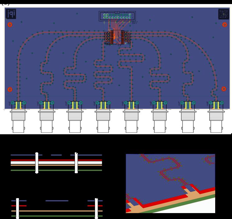
FIG. 3. (a) Breakout board layout. Signals enter the
board through the 20-pin connector at the top. Meanders
help equalize electrical delays of all traces. (b) Stack-up of
FIG. 2. Termination networks used to interface the FPGA the PCB for the coplanar waveguide (c) Stack-up of the PCB
logics with external signals. (a) shows the circuit used for the for the microstrip below the BNC connector. (d) Close-up
four digital inputs on the carrier board while (b) shows the perspective view of the circuit board layout. Figure is not to
circuit used for the 64 digital outputs. scale.4
using a SMA to BNC adapter and compare the two TDR
responses. Four different sections can be distinguished
in the traces in Fig. 4: the SMA connector, the BNC
adapter, the coplanar waveguide on the PCB, and the
output buffer passive impedance. Apart from the output
buffer, which shows a change of impedance compatible
with a capacitive load, the maximum impedance varia-
tion for the BNC connector and coplanar waveguide de-
sign is below ≈ 10%, limiting reflections below ≈ 5%.
IV. FIRMWARE DEVELOPMENT
FIG. 4. Time Domain Reflectometry measurement of the A. Communication
breakout board. The characteristic impedance of the BNC
connector and coplanar waveguide remain within 10% of the To communicate instructions to the PSoC, we open a
50 Ω target value.
socket server on the PS. We then wait for the TCP/IP
client on the lab computer to connect. Once the connec-
tion is established, data is sent through the socket stored
software. in a numpy array34 , which is mapped on a contiguous
Fig. 3(a) shows how the eight coplanar waveguides are section of SDRAM shared with the PL through a DMA
arranged on the breakout board. To prevent variations in controller. The data is then accessed by the PL and pro-
the timing delay across different output channels, we have cessed by the state machine as instructions in a 128 bit
matched the length of all 8 traces using meanders. Based format extension of the 80 bit long instruction format
on the information provided by the PCB manufacturer used in the PulseBlaster35 . In case the connection is un-
(nominal relative dielectric constant r = 4.3), we de- expectedly broken, we have implemented an algorithm
signed the coplanar waveguide, as illustrated in Fig. 3(b), for the server to automatically refresh the same socket
with a width W1 = 0.46 mm, spacing between traces and connection, instead of creating a new one. This makes
top-layer ground plane S1 = 0.3 mm, and separation from the system robust against the interruption of the connec-
top-inner-layer ground plane H1 = 0.24 mm. We chose tion without having to manually reset it.
edge-mount BNC connectors rated up to 4 GHz to mini-
mize the characteristic impedance discontinuity from the
PCB to the coaxial cables. For impedance matching,
the connectors need to be soldered to a microstrip that B. State Machine
ends at the edge of the PCB. However, to ensure an ad-
equate mechanical strength for the connector’s central To control the 64 TTL output channels, we have writ-
pin soldering joint, the width of the microstrip must be ten a Mealy36 state machine in the programmable logic
much larger than the width W1 = 0.46 mm of the copla- of the FPGA. In contrast with Moore37 state machines,
nar waveguide in Fig. 3(b). To allow for a wider section Mealy state machines’ inputs directly affect the outputs,
of the transmission line, we therefore remove the inner- allowing for a lower-latency design. We wrote our state
top ground layer from under the central pin’s soldering machine in System Verilog to take advantage of special-
pad, as shown in Fig. 3(c). Using the inner-bottom layer ized features of the language, such as enumeration logic
as the new ground plane, the distance from the trans- and the passing of structured data through design mod-
mission line is increased to H2 = 1.26 mm. A nominal ules. The state machine first fetches 128 bit instructions
50 Ω impedance is now obtained with W2 = 2.29 mm and from a 128x32768 RAM, mapped as shown in Fig. 5.
S2 = 1.27 mm. A perspective view of the PCB layers is There are five fields that make up the 128 bit instruction
shown in Fig. 3(d). to the state machine: time delay (32 bits), data (20 bits)
We verified the performance of the transmission lines opcode (4 bits), flags (64 bits) and finally the remaining 8
and BNC launch by performing a time domain reflec- bits are reserved for future use. The state machine reads
tometry (TDR33 ) measurement on the PCB. The result the memory bank row by row. The opcode tells the state
of the meaurement is shown in Fig. 4, where we use the machine which state to enter next, and the flags field des-
technique described in Ref.33 to measure the amplitude ignates which output channels will be changed or affected
of a reflected step signal to calculate the characteristic with each instruction. The data contains any special in-
impedance along a transmission line as a function of elec- formation specific to the current opcode. For example, if
trical delay. We first measure the response of a coaxial the state machine is being instructed to enter a loop, the
cable with an SMA (SubMiniature version A) connector data would contain the number of loop iterations. Fi-
attached to a SMA 50 Ω termination. We then connect nally, the ‘delay’ argument indicates how long the state
the coaxial cable to our PCB board, while not powered, machine should wait before loading the next instruction.5
FIG. 5. Illustration of the memory in the FPGA. The memory is split into Bank 0 and Bank 1, each with 16834 instructions.
The memory has a width of 128 bits. Each instruction contains 64 bits for the state of each of the flags, 4 bits for the opcode,
20 bits for the data argument, and 32 bits for the time delay argument. The last 8 bits are left unused, but can be allocated
in the future.
The states that we have programmed in our state ma- C. Ping-Pong Memory
chine are shown in Table I, along with the accompanying
‘data’ field. To facilitate integration with Labscript, we The state machine described in the previous section
choose an instruction set that is mostly compatible with is designed to read instructions from a 32768-instruction
the one of the Pulseblaster, which is extensively used static memory. To increase the available memory, we use
within the Labscript codebase (we did not implement the 32768-instruction space as a cache memory and di-
nested loops, as they are not used in Labscript). vide it into two banks with 214 = 16384 instructions each:
Bank 0 and Bank 1, as shown in Fig. 5. We then im-
plement a ping-pong memory controller to automatically
update the content of the memory by requesting direct
State Instruction Data Function memory access (DMA) to a large shared contiguous por-
0 CONTINUE None Continues to next
tion of the SDRAM, which has space for up to 8192000
instruction
1 STOP None Stops execution of instructions. The algorithm for the ping-pong memory
program controller is shown in Fig. 6(a). The controller begins by
2 LOOP Number of Specifies beginning of transferring 16384 instructions from SDRAM into Bank 0
desired loops, loop of the PL RAM and setting a register called “last_bank”
great than or
equal to 1. The main state machine then begins execut-
equal to 1
3 END LOOP Address of Specifies end of loop ing instructions from RAM, starting from Bank 0, while
beginning of loop the ping-pong memory controller constantly monitors the
4 JSR Address of first Jumps to a subroutine memory address. Each time the memory address is not in
subroutine the bank identified by the register “last_bank”, the pre-
instruction viously accessed bank is refreshed with new data from
5 RTS None Program execution
returns to instruction
the SDRAM and the value of “last_bank” is updated
after JSR was called at with the identifier of the currently accessed bank. Set-
the end of subroutine ting “last_bank” equal to 1 when the state machine starts
6 BRANCH Address in Program execution causes Bank 1 to be updated immediately after Bank 0 as
memory to branches to an address soon as the state machine accesses the memory. The PL
branch to specified by data
7 LONG Delay multiplier Executes the length of
RAM is a dual port memory that can be independently
DELAY instruction given in addressed from two different clock domains. Thus, the
the time field state machine controlling the 64 TTL outputs does not
multiplied by delay need to be synchronous with the rest of the PL and with
multiplier the PS. The ping-pong memory controller and DMA en-
8 WAIT None Waits for a hardware
trigger to continue
gine are clocked by the PS, while the state machine can be
program execution optionally clocked from one of the PLLs (Phase Locked
Loop) available in the PL fabric that can be locked to an
TABLE I. List of states that was programmed in the state external reference connected to one of the four available
machine with associated data field and description of the func- BNC inputs.
tion performed. The state numbering corresponds to the as- The automatic RAM refresh implemented by the ping-
sociated opcode. pong memory controller can pose a problem if certain in-6
number of instructions, without changing the final behav-
ior at run time. In the current Labscript driver, there is
only one instance where underflow can happen: when the
complex instruction called “reps” is translated into either
a LOOP immediately followed by an END LOOP instruc-
tion or a series of LOOP, LONG DELAY, END LOOP. To pre-
vent memory underflow, we have implemented checks in
the code while the program is compiling. The algorithm
is illustrated in Fig. 6(b). When a LOOP opcode is found,
the system checks if either the instruction is mapped on
the last instruction of a bank or if it is mapped on the
second to last and is immediately followed by a LONG DE-
LAY instruction. In these cases, it inserts additional CON-
TINUE instructions to ensure that the LOOP instruction
is moved to the beginning of the next bank. To ensure
that the insertion does not modify the original timing,
the field ‘delay’ in the LOOP instruction is reduced by
the duration of the inserted CONTINUE instructions.
V. DISCUSSION
The PSoC-based primary clock device, that we have
created for controlling AMO physics experiments, is eas-
ily integrated with the Labscript Suite. The hardware
provides 64 buffered digital outputs for controlling other
hardware devices and also 4 input trigger channels. The
printed circuit board design ensures signal integrity and
minimal crosstalk between channels. Our firmware de-
sign implements a state machine written in System Ver-
ilog and a ping-pong memory controller that allows the
execution of a large number of instructions (exceeding
8192000). The system is currently being used to run
the entire experiment in our lab, providing triggers for
digital to analog coverters (DAC), digital direct synthe-
FIG. 6. Bank switching and compiler check algorithms for sizers (DDS), mechanical shutters, and many other in-
the ping-pong memory controller. (a) The system begins struments.
by loading bank zero and setting the “last_bank” to Bank According to the Synthesis tools timing reports the
1. From there, the system consistently checks the memory maximum frequency the state machine can operate at is
address of the state machine to determine whether it has 104 MHz, and it is currently clocked at 100 MHz. There-
switched banks in the memory. If it has switched banks, fore, the current timing resolution is 10 ns, although using
it changes “last_bank” and loads the other bank of memory
serializers in the PL fabric would allow timing resolutions
with new instructions. (b) Checks performed during com-
pilation to avoid memory underflow. The logic expressions
down to 1 ns. The versatility of the platform also allows
mem_addr % 214 > 214 − 2 and mem_addr % 214 = 214 − 1 for other modifications, such as the possibility to add
check, respectively, if mem_addr is mapped to the last two additional instructions to the state machine. For exam-
slots or the last slot in the memory bank (% is the MOD ple, an additional instruction could initiate a train of a
operator). specific number of pulses with an adjustable duty cycle
and period using a single instruction, rather than using
loops. Other extensions of the instruction set could al-
low for conditional branching, which has already been
structions span over two banks, such as LOOP/END LOOP, shown to be useful in ion trapping experiments38 . Fur-
BRANCH, JSR/RTS. For example, if a loop is started in the ther modifications to the design might include network
first bank, but ends in the second bank, since the first security protocols and encryption for data transmission,
bank is updated with new instructions while the second which we have not included since our setup is running
bank is running, the system will no longer have the ini- on an isolated network. A possible use of the system
tial loop instruction to refer back to. The compiler must we have considered, and have extensively taken advan-
be aware of this type of memory bank underflow or over- tage of during testing, is its capability to run scripts di-
flow and be able to resolve them by altering the order and rectly from the local Jupyter notebook server. With the7
Jupyter web interface, a remote computer is not neces- 12 B. S. Malek, Z. Pagel, X. Wu, and H. Müller, “Em-
sary for the generation of patterns, and the device can be bedded control system for mobile atom interferome-
used as a stand-alone testbench digital pattern generator. ters,” Review of Scientific Instruments 90, 073103 (2019),
https://doi.org/10.1063/1.5083981.
Our PSoC-based primary clock device has the capabil- 13 A. Bertoldi, C.-H. Feng, H. Eneriz, M. Carey, D. S.
ity to be integrated with many experimental setups with Naik, J. Junca, X. Zou, D. O. Sabulsky, B. Canuel,
minimal modification, and the whole design is available P. Bouyer, and M. Prevedelli, “A control hardware based
online39 . on a field programmable gate array for experiments in atomic
physics,” Review of Scientific Instruments 91, 033203 (2020),
https://doi.org/10.1063/1.5129595.
14 E. Perego, M. Pomponio, A. Detti, L. Duca, C. Sias,
ACKNOWLEDGEMENTS and C. E. Calosso, “A scalable hardware and software con-
trol apparatus for experiments with hybrid quantum sys-
tems,” Review of Scientific Instruments 89, 113116 (2018),
We thank Daniel Barker, Qi-Yu Liang, and Peter Elgee https://doi.org/10.1063/1.5049120.
for their careful reading of the manuscript. This work 15 S. Donnellan, I. R. Hill, W. Bowden, and R. Hobson, “A
was partially supported by the NSF through the Physics scalable arbitrary waveform generator for atomic physics ex-
periments based on field-programmable gate array technol-
Frontier Center at the Joint Quantum Institute. ogy,” Review of Scientific Instruments 90, 043101 (2019),
https://doi.org/10.1063/1.5051124.
16 A. Keshet and W. Ketterle, “A distributed, graphical user in-
DATA AVAILABILITY terface based, computer control system for atomic physics ex-
periments,” Review of Scientific Instruments 84, 015105 (2013),
https://doi.org/10.1063/1.4773536.
The data that support the findings of this study are 17 W. Lee, M. Park, S. Seo, and H. Kim, “New design approach of
available from the corresponding author upon reasonable fpga based control system and implementation result in kstar,”
Fusion Engineering and Design 88, 1338 – 1341 (2013), proceed-
request.
ings of the 27th Symposium On Fusion Technology (SOFT-27);
1 T.
Liège, Belgium, September 24-28, 2012.
Bothwell, D. Kedar, E. Oelker, J. M. Robinson, S. L. Bromley, 18 P. Kulik, G. Kasprowicz, and M. Gąska, “Driver mod-
W. L. Tew, J. Ye, and C. J. Kennedy, “JILA SrI optical lattice ule for quantum computer experiments: Kasli,” in Photon-
clock with uncertainty of 2.0 × 10⁻¹⁸ ,” Metrologia 56, 065004 ics Applications in Astronomy, Communications, Industry,
(2019). and High-Energy Physics Experiments 2018 , Vol. 10808 (In-
2 N. Hinkley, J. A. Sherman, N. B. Phillips, M. Schioppo, N. D.
ternational Society for Optics and Photonics) p. 1080845,
Lemke, K. Beloy, M. Pizzocaro, C. W. Oates, and A. D. Ludlow, https://doi.org/10.1117/12.2501709.
“An Atomic Clock with 10−18 Instability,” Science 341, 1215 19 Xilinx, “UG1144 petalinux tools documentation,” https:
(2013). //www.xilinx.com/support/documentation/sw_manuals/
3 J. I. Cirac and P. Zoller, “Goals and opportunities in quantum
xilinx2020_2/ug1144-petalinux-tools-reference-guide.pdf
simulation,” Nature Physics 8, 264–266 (2012). (2020, accessed January 28, 2021).
4 F. Verstraete, M. M. Wolf, and J. Ignacio Cirac, “Quantum com- 20 Yocto Project, “Open source embedded linux build system pack-
putation and quantum-state engineering driven by dissipation,” age metadata and sdk generator,” https://www.yoctoproject.
Nature Physics 5, 633–636 (2009). org/ (2020, accessed January 28, 2021).
5 J. Ye, H. J. Kimble, and H. Katori, “Quantum 21 T. Xue, H. Li, G. Gong, and J. Li, “Design of epics ioc based
state engineering and precision metrology using state- on rain1000z1 zynq module*,” Proceedings of ICALEPCS2015,
insensitive light traps,” Science 320, 1734–1738 (2008), Melbourne, Australia (2015).
https://science.sciencemag.org/content/320/5884/1734.full.pdf. 22 S. Lee, C. Son, and H. Jang, “Distributed and parallel real-
6 F. Sorrentino, A. Alberti, G. Ferrari, V. V. Ivanov, N. Poli,
time control system equipped fpga-zynq and epics middleware,”
M. Schioppo, and G. M. Tino, “Quantum sensor for atom-surface (2016) pp. 1–4.
interactions below 10 µm,” Phys. Rev. A 79, 013409 (2009). 23 Xilinx, “PYNQ python productivity for zynq,” https://github.
7 Certain commercial products or company names are identified
com/xilinx/pynq (accessed January 26, 2021).
here to describe our study adequately. Such identification is not 24 Avnet, “Microzed documentation,” http://zedboard.org/
intended to imply recommendation or endorsement by the Na- support/documentation/1519 (accessed January 26, 2021).
tional Institute of Standards and Technology, nor is it intended 25 Xilinx, “Document DS190, XC7000 series datasheet,”
to imply that the products or names identified are necessarily the https://www.xilinx.com/support/documentation/data_
best available for the purpose. sheets/ds190-Zynq-7000-Overview.pdf (2018, accessed Jan-
8 P. T. Starkey, C. J. Billington, S. P. Johnstone, M. Jasperse,
uary 26, 2021).
K. Helmerson, L. D. Turner, and R. P. Anderson, “A 26 A. Devices, “ADCMP552 datasheet,” https://www.analog.com/
scripted control system for autonomous hardware-timed exper- media/en/technical-documentation/data-sheets/ADCMP551_
iments,” Review of Scientific Instruments 84, 085111 (2013), 552_553.pdf (accessed February 3, 2021).
https://doi.org/10.1063/1.4817213. 27 Torex, “XCL214 datasheet,” https://www.torexsemi.com/file/
9 M. Patel, A. Sakaamini, M. Harvey, and A. J. Murray, “An
xcl213/XCL213-XCL214.pdf (accessed February 2, 2021).
experimental control system for electron spectrometers using ar- 28 ST Microelectronics, “STM6779 supervisor datasheet,” https:
duino and labview interfaces,” Review of Scientific Instruments //www.st.com/resource/en/datasheet/stm6720.pdf (2020, ac-
91, 103104 (2020), https://doi.org/10.1063/5.0021229. cessed January 28, 2021).
10 R. Hošák and M. Ježek, “Arbitrary digital pulse sequence gen-
29 Xilinx, “Zynq-7000 SoC datasheet,” page 8, https:
erator with delay-loop timing,” Review of Scientific Instruments //www.xilinx.com/support/documentation/data_sheets/
89, 045103 (2018), https://doi.org/10.1063/1.5019685. ds187-XC7Z010-XC7Z020-Data-Sheet.pdf (2020, accessed
11 P. E. Gaskell, J. J. Thorn, S. Alba, and D. A. Steck, January 28, 2021).
“An open-source, extensible system for laboratory timing and 30 Texas Instruments, “SN74S244DWG4 datasheet,” https://www.
control,” Review of Scientific Instruments 80, 115103 (2009), ti.com/lit/ds/symlink/sn74s244.pdf (2016, accessed January
https://doi.org/10.1063/1.3250825.8
26, 2021). 35 SpinCore, “Pulseblaster manual,” page 27, http://spincore.
31 Xilinx, “Xilinx user guide UG471 ver 1.10,” https: com/CD/PulseBlaster/PCI/PB24/PB_Manual.pdf (2020, accessed
//www.xilinx.com/support/documentation/user_guides/ January 28, 2021).
ug471_7Series_SelectIO.pdf (2018, accessed January 26, 36 G. H. Mealy, “A method for synthesizing sequential circuits,”
2021). The Bell System Technical Journal 34, 1045–1079 (1955).
32 Kicad, “PCB calculator user manual,” https://docs.kicad.org/ 37 E. F. Moore, “Gedanken-experiments on sequential machines,”
5.1/en/pcb_calculator/pcb_calculator.html (2019, accessed in Automata Studies, edited by C. Shannon and J. McCarthy
January 26, 2021). (Princeton University Press, Princeton, NJ, 1956) pp. 129–153.
33 B. M. Oliver, “Time Domain Reflectometry,” HP Journal 15(6) 38 K. E. Wright II, Manipulation of the Quantum Motion of
(1964). Trapped Atomic Ions via Stimulated Raman Transitions, Ph.D.
34 I. Idris, Learning NumPy Array. (Packt Publishing, 2014). thesis, University of Maryland (2017).
39 JQI, “Jqi automation for experiments (jane),” https://github.
com/JQIamo/jane (2021, accessed January 26, 2021).You can also read