Novel diffractive optical element: binary photon sieve - Changlun Hou - SPIE ...
←
→
Page content transcription
If your browser does not render page correctly, please read the page content below
Novel diffractive optical element: binary
                photon sieve

                Changlun Hou

Downloaded From: https://www.spiedigitallibrary.org/journals/Optical-Engineering on 17 Nov 2021
Terms of Use: https://www.spiedigitallibrary.org/terms-of-use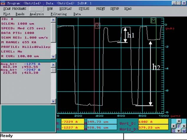
Optical Engineering 50(6), 068001 (June 2011)

                 Novel diffractive optical element: binary photon sieve
                 Changlun Hou                                                       Abstract. In this paper, we developed a novel photon sieve consisting of a
                 Zhejiang University                                                large number of precisely positioned holes distributed according to an un-
                 State Key Laboratory of Modern Optical                             derlying Fresnel zone plate (FZP) geometry, while the holes at transparent
                    Instrumentation                                                 and opaque circular rings of the FZP have a π phase shift. Compared to a
                 Hangzhou 310027, China                                             conventional photon sieve which we call an amplitude-photon sieve (PS),
                 E-mail: hou_cl@hotmail.com                                         the binary photon sieve has a transmission two times more amplitude-PS
                                                                                    and a diffractive efficiency approximately four times than amplitude-PS. A
                                                                                    70-mm diameter, f/10 binary photon sieve has been fabricated for opera-
                                                                                    tion at visible light. Details of design, fabrication, and performance of the
                                                                                    binary photon sieve are presented.    C 2011 Society of Photo-Optical Instrumentation

                                                                                    Engineers (SPIE). [DOI: 10.1117/1.3589294]

                                                                                    Subject terms: photon sieve; diffractive optics; binary optics; micro-optics.
                                                                                    Paper 101035RR received Dec. 7, 2010; revised manuscript received Mar. 28,
                                                                                    2011; accepted for publication Apr. 14, 2011; published online Jun. 6, 2011.

                 1 Introduction                                                                   the fabrication of a single surface without any supporting
                 The photon sieve (PS) is a diffractive element which is de-                      struts required. Recently, by combining the concepts of the
                 rived from a traditional Fresnel zone plate (FZP) and con-                       Fractal zone plate (FraZP) and the photon sieve, the fractal
                 sists of millions of pinholes distributed on transparent cir-                    photon sieve (FraPS)7–9 has been developed which not only
                 cular rings of FZP. Compared with FZP, a large number of                         has similar unique properties as FraZPs but also significantly
                 holes distributed appropriately over the Fresnel zones make                      suppress the high order diffractions.
                 it possible to focus light to a spot size smaller and the higher                     In the case of amplitude photon sieves, only the pinholes
                 order of diffraction and secondary maxima can be suppressed                      distributed on corresponding transparent circular rings of
                 significantly. In addition, photon sieve provides the advan-                     FZP are transparent, so the focusing efficiency of such a
                 tage that the size of the focused spot is not limited by the                     photon sieve is lower than the FZP with the same diameter
                 width of the smallest zone. As in the case of traditional FZP,                   and focal length. It is significant to improve the focusing ef-
                 the spatial resolution that can be achieved is of the order of                   ficiency of the photon sieve especially for its use on a high
                 the width of the outermost zone and is therefore limited by                      resolution system such as a lithography system and a tele-
                 the smallest structure that can be fabricated by lithography.                    scope system. In order to improve efficiency based on photon
                 The size of the holes can be increased beyond the underlying                     sieve and binary optics element, we developed a new type
                 zone width to permit the construction of a large optic with                      of photon sieve which we call binary photon sieve. In the
                 holes of a reasonable size at the outermost zones within the                     binary photon sieve, millions of holes are distributed on cor-
                 aperture.1 The increase in hole diameters greatly reduces the                    responding transparent and opaque circular rings of Fresnel
                 design constraints on fabricating such a device. It is espe-                     zone-plates, while holes in alternate zones have a π phase
                 cially important when the width of the zone approaches the                       shift. By appropriately placing the holes in the transparent
                 lithographic limits.                                                             and opaque zones, the zero-order diffraction efficiency will
                     These characters of the photon sieve show that it has a                      be significantly reduced, and consequently, the focusing ef-
                 promising future in high resolution imaging and super nar-                       ficiency will be enhanced.
                 row width lithography areas. Kipp and his colleagues pre-
                 sented the concept of the photon sieve.1 They use a pinhole                      2 Theory
                 distributed on the Fresnel zone to focus a soft x-ray onto                       Figure 1 shows the amplitude-PS and binary photon sieve.
                 a spot which was smaller than the width of the outermost                         On the amplitude-PS, holes are distributed on transparent
                 zone of the Fresnel zone. Menon et al. used a photon sieve                       circular zones, while on the binary photon sieve, holes are
                 in their lithography system as the focus lens. The numeri-                       distributed not only on transparent circular zones, but also
                 cal aperature (NA) of their photon sieve can reach 0.9 and                       on opaque circular zones. The holes at transparent circular
                 the width of the exposure line can reach 244 nm at 400-nm                        zones and opaque circular zones have a π phase shift.
                 wavelength.2, 3 Andersen and his colleagues fabricated a 1-m                        Cao and Jahns have built a model based on the far-field
                 focal length, 0.1-m diameter photon sieve over a significant                     formula of individual pinholes and the linear superposition
                 bandwidth and had a moderate field of view. They pointed                         principle which is applicable to arbitrary paraxial illumi-
                 out that PS offers an appealing solution for the construction                    nation with arbitrary complex amplitude distribution at the
                 of next-generation, ultralarge space telescope primaries.4–6                     photon sieve plane.10, 11 Assume a binary photon sieve, which
                 They also said that a flat element can be simply packaged                        consists of a great number of pinholes whose locations and
                 and deployed without the problems associated with creat-                         radii are properly chosen, is located at the xy plane. The de-
                 ing a diffraction-limited, three-dimensional mirror surface                      sired focal point is located at the point (X = 0, Y = 0), the
                 and the photon sieve has no connected regions which permit                       phase shift is between transparent and opaque zones is π ,
                                                                                                  and the distance between the xy plane and the XY plane is
                0091-3286/2011/$25.00
                                      C 2011 SPIE                                                 q. Because the change of the field inside the pinhole is very

                 Optical Engineering                                                      068001-1                                                  June 2011/Vol. 50(6)

Downloaded From: https://www.spiedigitallibrary.org/journals/Optical-Engineering on 17 Nov 2021
Terms of Use: https://www.spiedigitallibrary.org/terms-of-use
Hou: Novel diffractive optical element: binary photon sieve

                 Fig. 1 (a) Schematic of amplitude-PS and (b) binary photon sieve.                Fig. 3 Photograph of the fabricated binary photon sieve. (a) Zoom
                                                                                                  30×, (b) zoom 100×.

                small, the complex amplitude distribution inside the pinhole                         Assume the n’th pinhole, whose central location and ra-
                can be expressed as the local plane wave. Assume the lo-                          dius are denoted by (x = xn , y = yn ) and an , respectively.
                cal plane wave is the normal illumination. We denote by                           Equations (1) and (2) can be derived as follows:10, 11
                A(x, y)exp[jkL(x, y)] the complex amplitude distribution of

                the paraxial illumination beam at the photon sieve plane,                                                              R2             kan
                                                                                                  Un (X, Y ) = 2N f An exp jk L n +            Jinc       ·ρ ,
                where k = 2π /λ is the wave number, λ is the wavelength, j is                                                          2q               q
                the imaginary unit, L(x, y) is the eikonal, and A(x, y) is the real
                amplitude. From the Fresnel diffraction integral formula, the                                                                                           (4)
                corresponding diffracted field Un (X, Y ) at transparent circu-                   where R =
                                                                                                                      (X − xn )2 + (Y − yn )2 ,
                lar zones can be expressed as:
                                   ∞                                                            ρ=
                              1
                Un (X, Y ) =              A(x, y) exp [ jk L (x, y)]
                             λq       −∞                                                             (X − xn − q(∂ L/∂ x)|xn ,yn )2 + (Y − yn − q(∂ L/∂ y)|xn ,yn )2 ,

                                         (X − x)2 + (Y − y)2                                      L n = L(xn , yn ), Jinc(t) = Jn (t)/t, Jn (t)is the n’th-order
                             × exp jk                              d xd y.      (1)
                                                    2q                                            Bessel function, and N f = πan2 /(λq) is the Fresnel number.
                                                                                                     The crucial idea of the photon sieve is that all those in-
                   The corresponding diffracted field Um (X, Y ) at opaque                        dividual diffracted fields from different holes have the same
                circular zones can be expressed as:                                               phase value or have a phase difference of 2 m π at the desired
                                   ∞                                                            focal point (X = 0, Y = 0). Therefore the selection condition
                               1
                Um (X, Y ) =             A(x, y) exp [ jk L (x, y)] exp( jπ )                     of the pinholes can be briefly stated as follows:
                              λq     −∞
                                                                                                              rn2                      kan
                                       (X −x)2 +(Y − y)2                                          k Ln +              = 2mπ,      Jinc       Rn     > 0,              (5)
                             × exp jk                        d xd y.        (2)                                 2q                        q
                                               2q
                                                                                                                rn2                               kan
                                                                                                  k Ln +              = (2m + 1)π,       Jinc         Rn   < 0,       (6)
                    In Eqs. (1) and (2), we have ignored the common factor -j                                   2q                                 q
                exp(jkq) for simplicity. According to the linear superposition
                principle, the total diffracted field U (X, Y ) at the focal plane                where rn2 = xn2 + yn2 ,
                is the sum of those individual diffracted fields from different
                pinholes, as the following equation shows:                                        Rn =     (xn + q(∂ L/∂ x)|xn ,yn )2 + (yn + q(∂ L/∂ y)|xn ,yn )2 .

                U (X, Y ) =       Un (X, Y ) +       Um (X, Y ).                (3)
                                  n                   m

                                                                                                  Fig. 4 Step height tested by profiler (h1 is the thickness of the chrome
                          Fig. 2 Fabrication process of binary photon sieve.                      layer and h2 is the step height of the adjacent pinholes).

                Optical Engineering                                                       068001-2                                                  June 2011/Vol. 50(6)

Downloaded From: https://www.spiedigitallibrary.org/journals/Optical-Engineering on 17 Nov 2021
Terms of Use: https://www.spiedigitallibrary.org/terms-of-use
Hou: Novel diffractive optical element: binary photon sieve

                 Fig. 5 (a) Photograph of photon sieve illuminated from the rear.
                 (b) Interferogram of the photon sieve.

                    The above derivation is based on paraxial Fresnel diffrac-
                 tion integral. The 4th order and higher order phase items in
                 spherical phase factors were neglected. This method is fit for
                 a low NA photon sieve; while for a high NA photon sieve,
                 the derivation should be based on a nonparaxial far field
                 model. Specially when the scales of pinhole is close to or
                 even smaller than the diffracted wavelength, a rigorous vec-
                 tor diffraction model such as rigorous coupled wave (RCW)                        Fig. 6 Wavefront measured by zygo interferometer. (a) Wavefront of
                                                                                                  amplitude photon sieve, (b) wavefront of binary photon sieve.
                 and modal approach should be used.

                                                                                                  Fig. 3(b), the circles with white margin are the pinholes with
                 3 Experimental Results and Discussion                                            an etched depth by the RIBE device.
                 We designed a 70-mm diameter, f/10 binary photon sieve.                             Figure 4 shows the step height of the pinholes at adjacent
                 By theoretical analysis, the diameter of the pinholes from the                   circular zones tested on a profiler (VEECO DEKTAK 3).
                 center to the edge ranged from 279.4 to 3.5 μm. Two 4 in.                        The fabricated step height of the pinholes at adjacent circular
                 masks were designed to fabricate the binary photon sieve.                        zones is 600.2 nm and the thickness of the chrome layer is
                 On mask 1, there are a large amount of pinholes distributed                      about 140 nm.
                 on corresponding transparent circular zones appropriately.                          The refractive index of the substrate material is 1.515 at
                 On mask 2, there are a large amount of pinholes distributed                      wavelength 650 nm. In order to get a π phase shift at adjacent
                 on corresponding opaque circular zones appropriately. As                         zones, the depth of the step can be calculated as:
                 shown in Fig. 2(a), a glass (K9) plate coated with a 140-nm
                                                                                                          λ            650
                 thick chrome layer was used as a substrate. First, by lithog-                    h=             =               = 631 nm,                           (7)
                 raphy and wet etching, the figures on mask 1 were replicated                          2×(n − 1)   2×(1.515 − 1)
                 on the substrate [as shown in Figs. 2(b)–2(f)]. Cerium ammo-
                 nia nitrate [Ce(NH4 )2 (NO3 )6 ] solution was used to etching                             631 − 600.2
                 chrome layer [as shown in Fig. 2(e)]. Secondly, the same                         h Error =               = 4.88%.                            (8)
                                                                                                                631
                 process was done on the substrate with mask 2 [as shown in
                 Figs. 2(g)–2(j)]. At the last step, by the reaction ion beam                     Because of the instability of the RIBE process caused by
                 etching process (RIBE) [as shown in Fig. 3(k)], a step will                      the reaction gas during the etching process, there is an error
                 appear between the holes replicated from mask 1 and mask 2.                      between the real depth and the theoretical depth. As shown
                 The step height was decided by the designed wavelength and                       in Eq. (8), the relative error is 4.88%. The fabrication error
                 the refractive index of the substrate material.                                  will cause the diffraction efficiency to deduce and bring some
                    All the lithography processes were performed on a 70-cm                       background scatter light.
                 glass substrate plate, spin coated with 800 nm of AZ4620                            From the distribution of the transparent area, a zone plate
                 (spun at 2500 rpm and baked on a hot plate at 90 ◦ C for                         has a transmission of 50%, whereas an amplitude photon
                 30 min).                                                                         sieve transmits only 15% to 25% of the incident light.1 A
                    Figures 3(a) and 3(b) show the photographs taken by a                         binary photon sieve can transmit double of the conventional
                 stereo microscope of the fabricated binary photon sieve. In                      photon sieve. In order to measure the diffractive efficiency
                                                                                                  of a binary photon sieve and an amplitude photon sieve, a

                                        Table 1 Experiment data.

                 Focus element           Measured intensity          Diffraction efficiency

                 Lens                         1.32 mW                        100%

                 Amplitude-PS                 38.82 μW                       2.94%

                 Binary-PS                   157.14 μW                      11.90%                Fig. 7 Images at the focal spot [(a) focal spot of binary photon sieve,
                                                                                                  (b) focal spot of amplitude photon sieve].

                 Optical Engineering                                                      068001-3                                                 June 2011/Vol. 50(6)

Downloaded From: https://www.spiedigitallibrary.org/journals/Optical-Engineering on 17 Nov 2021
Terms of Use: https://www.spiedigitallibrary.org/terms-of-use
Hou: Novel diffractive optical element: binary photon sieve
collimated laser beam was illuminated on the binary photon resolution imaging and super narrow width lithography
sieve and amplitude photon sieve, respectively, at the focal areas. For example, binary photon sieves have the poten-
plane a corresponding focal spot can be observed. tial to be primary elements in large space telescopes as they
Equation (9) was used to calculate the diffractive effi- can be constructed from flat membranes. For the diffractive
ciency by light intensity at the focal point and the incident element suffered from large amounts of dispersion, how to
intensity of the light: compensate for the dispersion will be a key problem in the
IFocus telescope design.
ηdiff = ×100%, (9)
IIncident
Acknowledgments
where ηdiff is diffractive efficiency, IFocus is the light intensity
at the focal point, and IIncident is the intensity of the light This research was supported by the National Science Founda-
illuminating on the photon sieve. tion (Grant No. 60908025). The authors would like to thank
From the experiment data (in Table 1), we can calculate Dr. Xu Jianfeng for the help on the RIBE fabrication process.
that the diffractive efficiency of the amplitude photon sieve
is 2.94% while the diffractive efficiency of the binary photon
References
sieve is 11.90%. The binary photon sieve has a diffractive
efficiency about 4 times that of the amplitude photon sieve. 1. L. Kipp, M. Skibowski, R. L. Johnson, R. Berndt, R. Adelung, S. Harm,
and R. Seemann, “Sharper images by focusing soft x-rays with photon
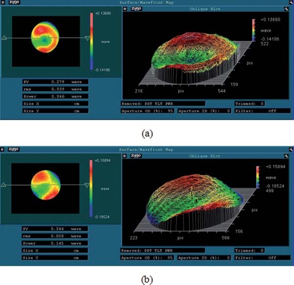
Figure 5 shows the measurement photograph of the bi- sieves,” Nature (London) 414, 184–188 (2001).
nary photon sieve on our zygo interferometer. Figures 6(a) 2. R. Menon, D. Gil, G. Barbastathis, and H. I. Smith;, “Photon-sieve
and 6(b) show the transmission wavefront of the amplitude lithography,” J. Opt. Soc. Am. 22(2), 342–345 (2005).
3. D. Gil, R. Menon, and H. I. Smith, “The case for diffractive optics
photon sieve and the binary photon sieve tested by the zygo in maskless lithography,” J. Vac. Sci. Technol. B 21(6), 2810–2814,
interferometer. The tested PV and rms values of the ampli- (2003).
4. G. Andersen, “Large optical photon sieve,” Opt. Lett. 30(22),
tude photon sieve are 0.279 and 0.039 λ and the tested PV 2976–2978 (2005).
and rms values of the binary photon sieve are 0.344 and 5. G. Andersen, “Photon sieve null corrector,” Proc. SPIE 6273, 62730K1
0.058 λ. (2006).
6. G. Andersen and D. Tullson, “Photon sieve telescope,” Proc. SPIE 6265,
Figures 7(a) and 7(b) show the focal spot of the amplitude 626523 (2006).
and binary photon sieves. The model of the CMOS camera 7. F. Giménez, J. A. Monsoriu, W. D. Furlan, and A. Pons, “Fractal photon
is MV-300UC with a pixel array of 2048×1536. The size sieve,” Opt. Express 14(25), 11958–11963 (2006).
8. F. Gimenez, W. D. Furlan, and J. A. Monsoriu, “Lacunar fractal photon
of each pixel is 3.2 × 3.2 μm. In the focal spot image of sieves,” Opt. Comm. 277, 1–4 (2007).
the amplitude photon sieve, the diameter of the focal spot is 9. Y. J. Liu, H. T. Dai, X. W. Sun, and T. J. Huang, “Electrically switchable
phase-type fractal zone plate and fractal photon sieves,” Opt. Express
5 pixels, and in the focal spot image of binary photon sieve, 17(15), 12418–12423 (2009).
the diameter of the focal spot is appreciably more than 10. Q. Cao and J. Jahns, “Focusing analysis of the pinhole photon sieve:
5 pixels. individual far-field model,” J. Opt. Soc. Am. A 19(20), 2387–2393,
(2002).
11. Q. Cao, “Diffractive nano-focusing and nano-imaging,” Proc. SPIE
4 Conclusion 6342, 634219 (2006).
In summary, we developed a new type of photon sieve which
can be regarded as a quasiphase-type photon sieve. The de-
Changlun Hou is a research member in
sign and fabrication process of the binary photon sieve was the Department of Optical Engineering and
introduced. A 70-mm diameter, f/10 binary photon sieve State Key Laboratory of Modern Optical In-
was fabricated. From the measured results of transmitted strumentation at Zhejiang University where
wavefront and focal spot of binary photon sieve and ampli- his work focused on optical measurement
tude photon sieve, we can conclude that the binary photon technology and micro-optics sensor. He re-
ceived a PhD degree in optical engineering
sieve has the same imaging and focus property with a am- from Zhejiang University in 2005 in China.
plitude photon sieve while the binary photon sieve demon-
strated a much higher diffractive efficiency (about 4 times)
than amplitude-type counterparts. They can be used in high
Optical Engineering 068001-4 June 2011/Vol. 50(6)
Downloaded From: https://www.spiedigitallibrary.org/journals/Optical-Engineering on 17 Nov 2021
Terms of Use: https://www.spiedigitallibrary.org/terms-of-useYou can also read


