NOC BASED DISTRIBUTED PARTITIONABLE MEMORY SYSTEM FOR A COARSE GRAIN RECONFIGURABLE ARCHITECTURE
←
→
Page content transcription
If your browser does not render page correctly, please read the page content below
2011 24th Annual Conference on VLSI Design

                 NoC Based Distributed Partitionable Memory
                  System for a Coarse Grain Reconfigurable
                                Architecture
                                 Muhammad Adeel Tajammul,                                               Sridharan Moorthi
                             Muhammad Ali Shami, Ahmed Hemani                                           NIT,Trichy,India
                                Royal Institute of Technology,Sweden                                Email: srimoorthi@nitt.edu
                                Email: tajammul,shami,hemani@kth.se

           Abstract—This paper presents a Network-on-Chip based dis-                    Streaming: Individual partitions composed of memory
        tributed partitionable memory system for a Dynamic Reconfig-                  banks (mBanks) should be able to act as a unit and stream
        urable Resource Array (DRRA). The main purpose of this design                data to the computational units. These streams have a generic
        is to extend the Register File (RFile) interface with additional
        data handling capability. The proposed interconnect which en-                timing model in the form of an initial delay, an intermittent
        ables the interaction between existing partition of computation              delay between successive read/writes and an end delay. These
        fabric and the distributed memory system is programmable and                 delay values can be adjusted according to intermediate results
        partitionable. The system can modify its memory to computation               to make the streams elastic.
        element ratio at runtime. The interconnect can provide multiple                 Performance and Energy: The memory architecture should
        interfaces that can support upto 8 GB/s per interface.
                                                                                     have extremely high bandwidth and very low latency. The
                                                                                     distributed nature of memory architecture and the concept
                                I. I NTRODUCTION
                                                                                     of private execution environments enable a short distance
           DRRA is a Coarse Grain Reconfigurable Architecture                         between storage and computation, which in turn contributes to
        (CGRA) capable of hosting multiple, complete Radio and                       low latency. The proposed design deploys wide interconnects
        Multimedia applications. It has resources for physical layer                 to achieve bandwidth upto 8 GB/sec per RFile to mBank
        (PHY layer), Protocol Processing layers (PP layer), application              interconnect. In addition, the distributed nature of DiMArch
        and system control and runtime management. The DRRA                          and PREX offers effective power management by allowing the
        fabric for the PHY layer has been implemented in [1] [2]                     unused mBanks to shutdown or put into low power mode.
        and is shown in Figure 1 along with the proposed memory                         Scalability: The DiMArch is scalable with the size of
        system. The DRRA PHY layer fabric will be briefly described                   memory partitions and clock frequency. The circuit-switched
        in section III as the DRRA architecture. A single DRRA                       segments of the data Network-on-Chip (dNoC) can be option-
        cell is composed of a morphable DataPath Units (mDPU), a                     ally pipelined.
        Register Files (RFile), a sequencer and an interconnect scheme                                   II. R ELATED W ORK
        gluing these elements together. At present, the storage of                      Reconfigurable architectures of the past decade are inves-
        DRRA fabric is restricted to RFiles which are 64 words of                    tigated for memory organization in [3]. Lambrechts et al.
        16 bits. This paper presents an on-chip distributed memory                   [4] investigates power and performance for multiple forms
        architecture for the PHY layer of DRRA with the following                    of interconnect. The design proposed in this paper is very
        salient features:                                                            similar to b-neg design in [4]. The programmable pipelined
           Distributed: DRRA being a fabric, the computation is                      and private partitioning differentiate the proposed design from
        distributed across the chip. Multiple threads, algorithms and                [4]. Further, the control traffic is routed over bus network as it
        applications are intended to run in parallel. To achieve true                has lower traffic. Data traffic is routed over the crossbar with
        parallelism it is essential to parallelize not only computation              programmable pipelined interconnects. Memory systems for
        but also the interconnect and access to memory. With dis-                    MP-SoCs can be either caches or scratch-pad based memory
        tributed memory, the proposed design enables multiple private                systems. Marescaux [5] provides a case where scratch-pad
        and parallel execution environments (PREX).                                  memory systems behave superior to cache based systems.
           Partitioning: The proposed Distributed Memory Architec-                      Morphosys [6] provides a set of frame buffers for parallel
        ture (DiMArch) is partitionable. Moreover, the architecture is               load/store of data between reconfigurable cells. As the size of
        designed to keep the cost of partitioning and re-partitioning                frame buffer is fixed, the memory element to computational
        low both in terms of cycles and energy. Partitioning is also a               element ratio remains fixed.
        distributed exercise and it happens in parallel which not only                  Imagine [7] provides a three stage memory architecture,
        speeds up partitioning but also enables runtime re-partitioning.             where the third stage is an off-chip memory. Beside a Local

       1063-9667/11 $26.00 © 2011 IEEE                                         232
       DOI 10.1109/VLSID.2011.45

Authorized licensed use limited to: NATIONAL INSTITUTE OF TECHNOLOGY SURATHKAL. Downloaded on March 26,2021 at 05:21:04 UTC from IEEE Xplore. Restrictions apply.
Register File (LRF), a scratch pad memory and a single Stream                has two comparators, one for each output and a counter.
        Register File (SRF) is connected as a second stage memory.                   The results of comparators, counter and overflow, underflow
        A single SRF is shared by multiple clusters but the ratio of                 are logged in a status word read by sequencer. mDPU can
        computational element to the storage resources remains fixed.                 do saturation, truncation/rounding, overflow, underflow check.
           SMART CELL [8] describes an innovative reconfigurable                      The end result bit-width can be configured to be anything from
        architecture with distributed data and instruction memory                    8 to 16 bits. RFile - the DRRA Register File is 64 word 16
        architecture. These memory units are directly connected to                   bit register file with dual read and write ports. RFile has a
        processing elements. Each mBank is 1K and works as a scratch                 DSP style AGU(Address Generation Unit) with vectorized,
        pad memory. Unlike SMARTCELL, the proposed architecture                      circular buffer and bit reverse addressing that is useful in
        can have array of memories assigned to a single mDPU                         implementing FFT. Each of these modes can be executed
        without any cost on performance of other mDPUs.                              once or in an endless loop. Each mode can have an arbitrary
           MONTIUM Tile processor [9] has a local memory for                         initial delay, a loop delay between each read/write and an
        each tile processor. Each tile processor is then connected to a              end delay before the loop iterates. These delays can be used
        Network-on-Chip (NoC) which can bring data from an on-chip                   for synchronization among DSP functions, I/O and DSP rate
        memory via AHB-bridge interface. The local memory per tile                   change functions. Moreover, these delays can be dynamically
        remains fixed in each MONTIUM implementations [9] [10].                       computed at runtime and is the basis for providing highly
           The proposed memory system can change its memory to                       sophisticated elastic streaming functionalities. Adjacent RFiles
        computational resource ratio by changing its partitioning, as                can be daisy chained to implement a shift register for a highly
        discussed in section V.This memory system is integrated with                 parallel FIR filter.
        DRRA Architecture [1] [2] which is discussed in section III.                    Sequencer is a micro-coded sequencing machine that con-
        Further-more, if the system is running with variable clock,                  trols a single mDPU and a RFile and the switchbox. Sequencer
        then it can alter its critical path accordingly as discussed in              can be daisy chained to allow a single Sequencer to control
        section VI.                                                                  adjoining Sequencers within the sliding-window reach. This
           This paper is organized as follows: Section I and II present              concept is used to implement a hierarchy of controllers,
        introduction and the related work on memory models of                        for instance to implement Rx/Tx FSMs of a MODEM or
        the current CGRAs. Section III presents the computational                    encode/decode FSMs of a CODEC. With elastic streaming
        fabric, the Dynamic Reconfigurable Resource Array (DRRA)                      capability of RFile together with the proposed memory ar-
        architecture. The proposed memory system is explained in                     chitecture(described in section IV) the sequencers provide the
        section IV. Section V deals with the private execution of                    capability to implement chained elastic streaming functionali-
        multiple processes. The programmable pipelining feature is                   ties that matches very well the nature of most PHY layers for
        briefly discussed in section VI. The costs and overheads                      radio and multi-media applications.
        of the different components of the system are formulated                        The seamless sliding-window circuit-switched interconnect
        in section VII. Section VIII presents few case studies on                    fabric connects the fabric of mDPUs, RFiles and sequencers
        the proposed system. Finally, section IX summarizes with                     organized in two rows as shown in Figure 1. In principle,
        concluding remarks.                                                          multiple such rows can be organized but the present ex-
                                                                                     periments are based on outputs of mDPUs and RFiles are
                          III. DRRA A RCHITECTURE
                                                                                     carried by horizontal buses, 3 columns on each side. A circuit-
           DRRA is a Coarse Grain Reconfigurable Architecture and                     switched interconnect, at the intersection of horizontal and ver-
        the proposed memory system is shown in Figure 1. The                         tical buses, controlled by sequencer, selects the programmed
        computational portion [1] [2] is briefly described in this                    outputs from the horizontal buses and loads them onto the
        section. DRRA PHY resources are:                                             vertical buses that feeds the inputs of mDPUs and RFiles as
        1. morphable Data Path Unit (mDPU)                                           shown in Figure 1. Each column can reach 3 columns to the
        2. Register File (RFile)                                                     right and 3 columns to the left. Thus including the middle
        3. Micro-coded hierarchical sequencing machine (Sequencer)                   column, 7 columns constitute the window that seamlessly
        4. A Seamless, sliding-window, circuit-switched interconnect                 slides across each such 7 column window. With this scheme,
        fabric.                                                                      each mDPU and RFile input can receive data from the output
        mDPUs are native 16-bit integer units with four 16-bit inputs                of 14 mDPUs and 14 RFiles, including itself. The fabric can
        corresponding to two complex numbers and two 16-bit output                   be as large as the die allows; several thousand DRRA cells can
        corresponding to one complex number. mDPU provides a)                        be accommodated in a 45 nm 300 mm2 die. Figure 1 shows
        MAC, with internal and external accumulation. This MAC                       only a fragment for clarity.
        has an adder in front to optionally implement the symmetric                         IV. D ISTRIBUTED M EMORY A RCHITECTURE
        FIR MAC, where the coefficients of symmetric samples are
        added before multiplication by the co-efficient, b) half of                      The proposed Distributed Memory Architecture (DiMArch)
        radix-2 butterfly for real or imaginary number c) add, subtract               for DRRA extends [12] which is composed of (a) a set of
        trees - 4 input adders/subtracters, two 2-input add/subtract                 distributed memory banks (mBanks), (b) a circuit-switched
        trees, sum-of-difference, difference-of-sum etc. mDPU also                   data Network-on-Chip (dNoC) (that transports data between

                                                                               233

Authorized licensed use limited to: NATIONAL INSTITUTE OF TECHNOLOGY SURATHKAL. Downloaded on March 26,2021 at 05:21:04 UTC from IEEE Xplore. Restrictions apply.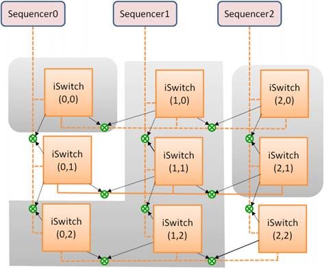
an end delay at the end of the loop before repeating the next
                                                                                     iterations. These delays are used to synchronize the memory
                                                                                     to register file streams with the computation. Individual delays
                                                                                     can be changed depending on the intermediate results of the
                                                                                     computation to make the streaming behavior elastic. mFSMs
                                                                                     are programmed via iNoC with special instructions.

                                                                                     B. Data Network-on-Chip (dNoC)
                                                                                        dNoC is a half-duplex circuit-switched mesh Network-
                                                                                     on-Chip. The streaming nature of applications, the inherent
                                                                                     QoS guarantees and improved latency compared to packet-
                                                                                     switched network were the motivations for using circuit-
                                                                                     switched network. A memory partition is defined as a set
                                                                                     of contiguous memory banks. A computation partition is
                                                                                     defined as a set of contiguous set of RFiles, mDPUs and
                                                                                     its associated sequencers and switchbox (see Figure 1). A
                                                                                     memory partition together with a computation partition is
                                                                                     called private execution environment (PREX). The interface
                                                                                     between memory and computational partition is as wide as the
                                                                                     number of RFiles involved; the width here implies the number
                                                                                     of dNoC connections, each dNoC being 256 bit wide, which
                                                                                     is a design time decision can be changed as it is a GENERIC
                                                                                     VHDL parameter in a template. Since the data traffic at each
                                                                                     RFile/dNoC (RFMI) interface can only be read or written, half-
                                                                                     duplex interconnects are proposed. dNoC is realized as a mesh
                                                                                     network of dSwitches. As shown in Figure 2, each dSwitch
                                                                                     is made up of five dSwitch cells (dCell) serving the N, E,
                                                                                     W, S and the mBank directions. Each dCell has four inputs
                                                                                     coming from the other four directions; one of these four inputs
                                                                                     is multiplexed out in the output mode; in the input mode,
                                                                                     data from the associated direction enters the dCell. The bi-
                              Fig. 1.   DRRA Architecture
                                                                                     directional I/O is optionally buffered to cope with long wires
                                                                                     and provide flexibility to implement the planned Dynamic
                                                                                     Voltage Frequency Scaling.
        mBanks and RFiles (DRRA Register Files)), (c) a packet-
        switched instruction Network-on-Chip (iNoC), a NoC and
        bus hybrid used to create partitions, program mBanks to
        stream data and transport instructions from sequencer to the
        instruction Switch (iSwitch).

        A. Memory Banks (mBank)
           As stated earlier, the DRRA memory architecture is realized
        as distributed memory banks that are SRAM macros, typically
        2 to 4 KB, a design time decision that is strongly influenced                                          Fig. 2.   dSwitch
        by the size of the DRRA cell (see Figure 1), as the goal                        cFSMs control the temporal behavior of dSwitch. They are
        is to align mBanks with the columns of the DRRA fabric.                      essential to make multiple mBanks behave as a contiguous
        mBanks are controlled by mFSMs - state machines that also                    memory. Figure 3 shows an example of a memory partition
        acts as interface between mBanks and the data Switches                       made up of three mBanks A, B and C that bring data to a single
        (dSwitch). mFSMs act as programmable address generation                      Register File (RFile) for processing and also take the data back
        unit with a general timing model. They implement single                      to the mBanks once processed. cFSMs associated with each
        read/write, vectorized read/writes with programmable address                 dSwitch are programmed to time multiplex the path to and
        offset, circular buffer and bit reversed addressing. Besides                 from register file in a co-ordinated way so that it appears as if
        the flexibility of typical DSP like address generation unit                   RFile is reading from/writing to one large contiguous memory.
        capability, mFSMs also provide a general purpose timing                      Compiler ensures that the computation is synchronized with
        model using three delays, an initial delay before a loop, an                 the behavior of cFSMs controlling the memory transactions.
        intermittent delay before every read or write within a loop and              This works fine for the targeted signal processing application

                                                                               234

Authorized licensed use limited to: NATIONAL INSTITUTE OF TECHNOLOGY SURATHKAL. Downloaded on March 26,2021 at 05:21:04 UTC from IEEE Xplore. Restrictions apply.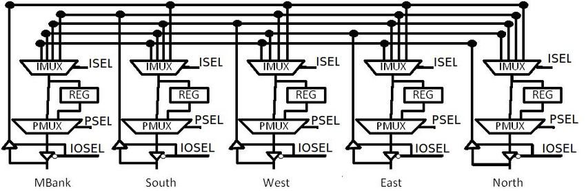
with deterministic cyclo-stationary behavior. The ability to                 targets hosting multiple applications(MODEMs and CODECs)
        partially reprogram these streams, allows these streams to be                simultaneously. So at first level, the iNoC split segments are
        elastic as well. The DRRA sequencers, the sequencers (see                    combined to enable each application to program in parallel
        Figure 1) have the hooks to chain these elastic streams but the              and allocate appropriate memory space. At second level, each
        present DiMArch does not support chained elastic streams.                    such application is very likely going to be implemented as
        The architecture can deal with the degenerate case of non-                   a pipelined datapath of functions like FFTs, FIRs, Viterbis
        deterministic random individual memory transactions as well                  etc. Each such function will have its own thread and set
        like a normal processor; this case will obviously not benefit                 of sequencers and they can program their memory partitions
        from the efficiency of autonomic (elastic) streaming capability               according to their need in parallel.
        of cFSMs in DiMArch. cFSMs are programmed by special
                                                                                        V. P RIVATE PARTITIONING OF MULTIPLE PROCESSES
        instructions via iNoC.
                                                                                        The concept of private partition is illustrated in Figure
                                                                                     4. Consider three Sequencers which need access to multiple
                                                                                     memory banks (mBanks). mBanks in the first row have
                                                                                     dedicated access from Sequencer in the same column. All
                                                                                     splitters are open at the start. Sequencers 1 and 2 issue an
                                                                                     instruction for respective instruction Switch (iSwitch) to close
                                                                                     vertical splitter for top-to-down access. Horizontal splitters
                                                                                     are set to remain open. Instruction Switch takes one cycle to
                                                                                     process this instruction. After a wait of one cycle, Sequencers
                                                                                     1 and 2 can now access iSwitches in second row (row 1). This
                            Fig. 3.   Single Memory Partition                        one cycle wait can be used to configure mFSM or cFSM for
        C. Instruction Network-on-Chip (iNoC)                                        required traffic patterns. Sequencer 1 issues another instruction
           iNoC is a packet-switched network used in DiMArch to                      for iSwitch (1, 1) to get access to iSwitch (1, 2). Sequencer 1
        program the cFSMs and mFSMs. The decision to use packet-                     issues instruction to close the vertical splitter top-down. Then
        switched network was taken because it is primarily used for                  Sequencer 1 instructs iSwitch (1,2) to close horizontal splitter
        short programming messages and life of a certain path is very                right-left between iSwitch (0,2) and iSwitch (1,2). At this point
        short. Additionally, the generality of packetized network to                 all sequencers have access to their desired private partitions.
        reach any node of the DiMArch from any sequencer. Even                          At run-time Sequencer 2 can gain access to iSwitch (2,2) to
        if iNoC is used to transport short programming messages,                     allocate more memory for additional memory requirements.
        agility of programming or reconfiguring DiMArchs partitions                   However, since the proposed architecture does not provide
        and behaviors is a key goal of the DRRA architecture to                      memory locks, all access conflicts are resolved at compile
        make it dynamically reconfigurable. To achieve this agility,                  time.
        while retaining the generality of packet-switched network, two                  When two PREX needs a shared memory space, then a
        architectural measures have been taken. The first is that the                 shared iSwitch is specified. e.g. Sequencer 0 and Sequencer
        horizontal and vertical segments of the iNoC are a hybrid                    1 can specify iSwitch (0,1) as a shared space. In that case,
        of bus and NoC behaviors. Any message asserted on an                         iSwitch(0,1) will receive instructions from both PREX. Fur-
        iSwitch is broadcast along its entire length of vertical segment,            thermore, the traffic for both cases should be deterministic and
        behaving like a bus as the broadcast happens in a single cycle.              conflicts are resolved at compile time.
        Every iSwitch on the vertical segment analyzes the message
        in parallel to check if the message address is on its associated
        horizontal segment and if it is, a second broadcast happens on
        the horizontal segment. Again, every iSwitch on the horizontal
        segment listens to the broadcast and analyzes if the message is
        addressed to it and if it is, it forwards it to zFSM that analyzes
        it and appropriately acts on it. By having a bus like behavior,
        the message is broadcast in a single cycle, i.e., each iSwitch
        can be reached in two cycles. The second measure to improve
        the agility of programming and re-programming is that these                                      Fig. 4.   Private Partitioning
        bus segments can be split to enable parallel programming of
        the split segments. Each horizontal and vertical segment can                              VI. P ROGRAMMABLE P IPELINING
        be potentially split with a simple message that toggles the split              Consider an example where three RFiles connected to nine
        status; initially all segments are split. So, the first action by the         MTiles in 3x3 configuration. For a single block transfer from
        sequencers is to combine the multiple segments horizontally                  mBank to RFile, mBank data is first sent to dSwitch. dSwitch
        or vertically by closing the splitters at appropriate places.                works either in pipelined or unpipelined mode. The pipelined
        This is explained with a simple example in section V. DRRA                   mode is used when PMUX is programmed to use the register

                                                                               235

Authorized licensed use limited to: NATIONAL INSTITUTE OF TECHNOLOGY SURATHKAL. Downloaded on March 26,2021 at 05:21:04 UTC from IEEE Xplore. Restrictions apply.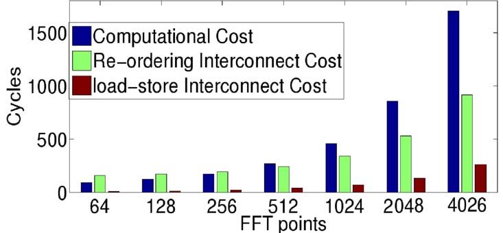
in its path (see Figure 2). The pipelined path is omitted                     reconfigured to change direction of instruction flow (or) 3.
        for Single Cycle Multi-Hop Transfer (SCMHT) mode. The                         computational fabric interconnects are reconfigured. The in-
        concerned dSwitch routes the data to neighboring dSwitch. At                  terconnect cost (CInterconnect ) depends on data transfers and
        destination, data is directly loaded into RFile from neighboring              is represented as:
        dSwitch. The number of cycles of each transfer is not always
                                                                                             CInterconnect = NT ransf ers ∗ CN um.of hops   (5)
        equal to the number of hops. The cycles may be reduced if
        any dSwitch is in SCMHT mode.                                                         NT ransf ers = N umber of T ransf ers
           The critical path for single cycle transfer for any given                  where
                                                                                              CN um.of hops = Cost in cycles/data transf er
        wireload model is variable; increase in number of hops will
        increase the critical path exponentially. So, increasing the                                             VIII. C ASE S TUDIES
        maximum number of hops in SCMHT mode will reduce the                          A. Mapping one dimensional point FFT
        clock speed of the system by the same rate. Hence, the number                    An implementation of radix-2 FFT butterfly was carried out
        of hops should only be increased for such cases when the gain                 in mDPU [1]. Four mDPUs are used to perform two butterfly
        of SCMHT mode is more than degradation due to lower clock                     operations (one real and one imaginary). The operations are
        frequency.                                                                    pipelined and are performed in six cycles. Depending on data
                   VII. S YSTEM C OSTS AND OVERHEADS                                  access patterns, the butterfly can be reused to implement vari-
           The system has three types of costs and overheads in-                      ous stages of FFT. Hence, an algorithm can be defined for FFT
        terms of cycles: 1. Computational Cost (CComputation ), the                   mapping by defining the traffic pattern between RFile, mBank
        time spent (cycles) in processing data by the DPU. 2. Re-                     and mDPU. In this case, FFT traffics are manually mapped. A
        configuration Overhead, the time which is required to re-                      maximum of sixteen butterflies are used in parallel. A single
        configure the interconnect partitioning. This time is directly                 butterfly is fed with data samples and twiddle factors from
        proportional to the number of splitters to be programmed.                     RFiles that can perform 32 operations in 40 pipelined cycles.
        Programming a single splitter takes three cycles (Instruction                 Between each FFT stage, reordering and reconfiguration is
        identification, Decoding and Partition set/reset). 3. Intercon-                performed. Reordering using the data Network is performed
        nect Overhead, deals with the amount of time (cycles) it takes                by common three stage data transfer. If the number of butterfly
        for the data to move between mBank and RFile.                                 operations per stage are more than the number of available
           All the costs and overheads are dependent on the method of                 butterflies, then additional butterflies are processed serially.
        its use. The computational cost is dependent on the mode of                   If re-ordering is required between neighbouring RFiles, then
        mDPU and data sample width since the mDPU is pipelined.                       interconnect reconfiguration is performed instead [2].During
        For example, cost of computation of an FFT butterfly using                     reordering the mBank truly behaves as a scratch-pad memory,
        two mDPUs is given by equation (1).                                           where intermediate data is stored.
                                                                                                     8000
                                                                                                            SmartCELL
              CComputation = (N.Sample /2) + OComputation          (1)                                      Morphosys
                                                                                                    6000   NoC
                NSample = N umber of Samples                                                                FPGA
        where                                                                                               DRRA
                                                                                            Cycles

                OComputation = Overhead of Computation                                               4000

        Overhead of computation is directly dependent on the mode
                                                                                                     2000
        of mDPU. The cost of pipeline (CP ipeline ) changes with each
        mDPU mode as number of stages of pipeline change.                                              0
                                                                                                            64   128    256     512 1024 2048 4096
                                                                                                                              FFT Point
                   OComputation = CP ipeline + CLoad         Store        (2)                                    Fig. 5.      FFT throughput
        where CLoad Store = RF ile load store Cost Computation
        Interconnect Reconfiguration cost (C.CIR ) is the cost of
        reconfiguration for the computational fabric which directly
        depend on the number of interconnects to reconfigure and the
        cost of reconfiguration. This cost can have the maximum value
        of six cycles.
                    CCIR = NInterconnect ∗ CComp.         Reconf          (3)
                                                                                                                  Fig. 6.     FFT Overhead
        mBank Interconnect Reconfiguration cost (CM IR ) directly                         First step in this mapping is loading the correct data in
        proportional to the number of instructions used to reconfigure                 the correct RFile. Data is loaded from the memory to all the
        the memory partitions (CP R ).                                                RFiles. By keeping a correct order at instruction level, data
                                                                                      is picked up by the correct RFile. Twiddle factors are also
                          CM IR = NInstruction ∗ CP R                     (4)         loaded to RFile which act as a Look Up Table (LUT). Figure
        Reconfiguration is performed when 1. new mBank is to                           5 extends the results of [11] for DRRA architecture. To keep
        be allocated, 2. the instruction partitioning interconnects are               the comparison fair, equal number of computational elements

                                                                                236

Authorized licensed use limited to: NATIONAL INSTITUTE OF TECHNOLOGY SURATHKAL. Downloaded on March 26,2021 at 05:21:04 UTC from IEEE Xplore. Restrictions apply.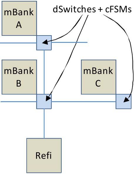
are used. The last two results for SMARTCell and FPGA are private partitioning capability where multiple sequencers can
interpolated based on [11]. The proposed system outperforms communicate with different mBanks using different segments
others by an order of magnitude more than the expected error of the network. The controllers within the system help in
in interpolation. For FFT larger than 512, the SmartCell is providing patterns of data which can be routed based on the
1.24 to 1.36 times slower than DRRA. instructions. The FFT and 2D experiments show the overhead
The implementations of FFT smaller than 512 on such of the interconnect, compared to the computational cost. The
parallel system do not exploit locality. Figure 6 illustrates that results show that for the given programmable interconnect the
the data for small-sized FFTs (less than 512) spends more best throughput is obtained when reasonable computational
time in motion rather than in computation. The memory-data resources are utilized with good locality to the data. Moreover,
interconnects overhead takes more or comparable times than gate-level synthesis results show that the system can run up-to
the time spent in computation. This can be further elaborated 400 MHz on 90nm technology.
by the fact that it takes marginally less cycles to compute the As a part of future work, another sequencer will be added
64 point FFT using a single butterfly (real and imaginary) set. which will act as a dedicated main controller for memory.
Such case uses 16 times less resources compared to the case The instruction memory topology will be investigated for Von
presented (16 butterflies). Neumann or Harvard architecture. More elaborate memory
mapping for video application can be explored. A compiler to
B. 2D Mapping vs McNoC [13]
automate the process of mapping is also under development.
The two dimensional FFT is performed in two steps.
First, row-wise FFTs are calculated. This step is followed by ACKNOWLEDGMENT
column-wise FFT calculation. Hence two dimensional FFTs The authors would like to thank the Higher Education
are broken down into multiple one-dimensional FFTs. It is Commission of Pakistan for funding this research.
mapped using the same principles as in section VIII-A. In
R EFERENCES
this experiment, the size of FFT remains constant and number
of resources are increased. Further more, an extra step is [1] M. A. Shami and A. Hemani, “Morphable dpu: Smart and efficient data
path for signal processing applications,” vol. SiPS, 2009, pp. 167–172.
added where horizontal to vertical translation is performed. [2] ——, “Partially reconfigurable interconnection network for dynamically
The results for such mapping are given in Figure 7. reprogrammable resource array,” in IEEE 8th International Conference
5
x 10
MCNoC/100
on ASIC (ASICON’09), 2009, pp. 122–125.
4
DRRA [3] M. Herz, R. Hartenstein, M. Miranda, and E. Brockmeyer, “Memory
3
addressing organization for streaming-based reconfigurable comput-
Cycles
2
ing,”Conference on Electronics Circuits and Systems, vol. 2, 2002,pp.
1
813–817.
0
4 8 16
Cells
32 64 [4] A. Lambrechts, P. Raghavan, M. Jayapala, B. Mei, F. Catthoor, and
Fig. 7. Cycle count for 2D-FFT D. Verkest, “Interconnect exploration for energy versus performance
tradeoffs for coarse grained reconfigurable architectures,”IEEE TRAN.
C. Mapping Matrix Multiplication VLSI Systems, vol. 17, no. 1, JANUARY 2009, pp. 151–155.
[5] T. Marescaus, E. Brockmeyer, and H. Corporaal, “The impact of higher
Consider a matrix multiplication of two matrix [64, 1]with communication layers on noc supported mp-socs,” in Proceeding of the
[1, 64] which results in [64, 64] matrix. Only such compu- First International Symposium on Network-on-Chip (NOCS’07), 2007,
tation require initial load and final store operations. All the pp. 107–116.
[6] H. Singh, L. Ming-Hau, L. Guangming, F. Kurdahi, N. Bagherzadeh,
multiplications are unique and can be performed completely and E. C. Filho, “Morphosys: an integrated reconfigurable system
parallel. The performance comparison between mapping on for data-parallel and computation-intensive applications,”IEEE TRAN.
proposed design and McNoC [13] is shown in Figure 8. The Computers, vol. 49, 2000, pp. 465–481.
[7] S. Rixner, W. J. Dally, B. Khailany, P. Mattson, U. J. Kapasi, and
variation in cost can be better understood by looking at the J. D. Owens, “Register organization for media processing,” in Sixth
overhead breakdown of such mapping given in Figure 9. When International Symposium on High-Performance Computer Architecture,
the decrease in computation cost is less than the increase in Jan. 2000, pp. 375–386.
[8] C. Liang and X. Huang, “Smartcell: A power efficient reconfigurable
interconnect cost, then it is feasible to parallelize such system. architecture for data streaming application,” in IEEE Workshop on Signal
Processing Systems (SiPS’08), 2008, pp. 257–262.
4000
MCNoC/100 2000 Computation Cost [9] G. Rauwerda, P. Heysters, and G. Smit, “Towards software defined
DRRA Interconnect Cost radios using coarse-grained reconfigurable hardware,”,IEEE TRAN. on
1500
Cycles
Cycles
2000 1000
VLSI, vol. 16, no. 1, 2008, pp. 3–13.
[10] L. Smit, A. Molclerink, P. Wolkotte, and G. Smit, “Implementation of 2-
500
d 8x8 idct on reconfigurable montium core,” in International Conference
0 0
1 2 4 8 16 on Field Programmable Logic and Applications, 2007, pp. 562–566.
1 2 4 8 16 Cells
Cells [11] C. Liang and X. Huang, “Mapping parallel fft algorithm onto smart-
Fig. 9. MM Overhead cell coarse-grained reconfigurable architecture,” in Proc. IEEE Design
Fig. 8. MM Cycles Automation Conference, 2001 , 2001, pp. 231–234.
[12] M.A. Tajammul, el. Al. “ A NoC Based Distributed Memory Archi-
IX. C ONCLUSION tecture with programmable and partitionable Capabilities,”NORCHIP
This paper proposes a programmable interconnect inter- 2010,Tampere Finland.
[13] X. Chen, Z. Lu, A. Jantsch, and S. Chen, “Supporting distributed
face as a method of communication between mBanks and shared memory on multi-core network-on-chip using a dual microcoded
RFiles. The programmable interconnect supports pipelined controller,”DATE 2010, pp. 39–44.
or bufferless modes. The instruction interconnect also has
237
Authorized licensed use limited to: NATIONAL INSTITUTE OF TECHNOLOGY SURATHKAL. Downloaded on March 26,2021 at 05:21:04 UTC from IEEE Xplore. Restrictions apply.You can also read