Negative index metamaterial at ultraviolet range for subwavelength photolithography
←
→
Page content transcription
If your browser does not render page correctly, please read the page content below
Nanophotonics 2022; 11(8): 1643–1651

Research Article

Qijian Jin, Gaofeng Liang*, Weijie Kong, Ling Liu, Zhongquan Wen, Yi Zhou, Changtao Wang,
Gang Chen and Xiangang Luo*

Negative index metamaterial at ultraviolet range
for subwavelength photolithography
https://doi.org/10.1515/nanoph-2022-0013                                     new insights into the manipulation of light. The improved
Received January 11, 2022; accepted February 27, 2022;                       working distance, well-shaped patterns over large area
published online March 15, 2022
                                                                             present an innovative method for improving subwavelength
                                                                             photolithography.
Abstract: A negative index metamaterial (NIM) at ultravi-
olet range is constructed with stacked plasmonic wave-                       Keywords: negative index metamaterial; plasmonic
guides. Based on the waveguides performing antisymmetric                     waveguide; subwavelength photolithography.
modes, the negative refractions of both wavevector and
energy flow are realized when a TM-polarized light with a
wavelength of 365 nm incidents on the plane of the layers.                   1 Introduction
It is proved that the NIM could be introduced into
subwavelength photolithography for extending working                         Nowadays, photolithography is one of the most important
distance. Both theoretical and experimental results indicate                 ways in fabricating integrated circuit and nano devices
that the patterns with a feature size of 160 nm can be                       [1, 2]. In particular, projection photolithography method
reproduced in photoresist with a 100 nm-thick air working                    can produce arbitrary patterns over large area with a single
distance. Moreover, arbitrary two-dimensional patterns with                  exposure process [3]. However, the resolution of traditional
a depth reach 160 nm can be obtained without diffraction                     photolithography is always blocked by the so-called
fringe by employing a nonpolarized light. This design gives                  diffraction limit due to the wave nature of light [4]. Even
                                                                             though the resolution can be improved remarkably by
                                                                             decreasing the working wavelength, using immersion
                                                                             lithography, or multipatterning process, these technolo-
*Corresponding authors: Gaofeng Liang, Key Laboratory of
                                                                             gies would involve much more complexity and cost. Hence,
Optoelectronic Technology & Systems (Chongqing University),
Ministry of Education, and College of Optoelectronic Engineering,            new cost-effective methods are needed to take the tech-
Chongqing University, Chongqing 400044, China,                               nique past the diffraction limit without huge expense.
E-mail: lgf@cqu.edu.cn. https://orcid.org/0000-0003-0817-7444;               Recently, various techniques have been developed for
and Xiangang Luo, State Key Lab of Optical Technologies on Nano-             pushing photolithography to higher resolution perfor-
fabrication and Micro-engineering, Institute of Optics and Electronics,
                                                                             mance, such as stimulated emission depletion lithography,
Chinese Academy of Sciences, Chengdu 610209, China,
E-mail: lxg@ioe.ac.cn. https://orcid.org/0000-0002-1401-1670
                                                                             absorbance-modulation optical lithography, photothermal
Qijian Jin, Key Laboratory of Optoelectronic Technology & Systems            lithography [5–7]. By contrast, near-field photolithography
(Chongqing University), Ministry of Education, and College of                is a straightforward way to produce subdiffraction limited
Optoelectronic Engineering, Chongqing University, Chongqing                  patterns by collecting the evanescent waves before they
400044, China; and State Key Lab of Optical Technologies on Nano-            decay [8]. In this instance, plasmonic lithography has been
fabrication and Micro-engineering, Institute of Optics and Electronics,
                                                                             developed attractively [9, 10]. This method would enhance
Chinese Academy of Sciences, Chengdu 610209, China
Weijie Kong, Ling Liu and Changtao Wang, State Key Lab of Optical            evanescent waves by exciting surface plasmons to
Technologies on Nano-fabrication and Micro-engineering, Institute of         compensate the decay and then lead to a super-resolution
Optics and Electronics, Chinese Academy of Sciences, Chengdu                 pattern. However, the photoresist (PR) has to be close
610209, China                                                                contacted to the plasmonic devices, while, direct-write
Zhongquan Wen, Yi Zhou and Gang Chen, Key Laboratory of
                                                                             lithography systems [11–13] do not meet the requirement of
Optoelectronic Technology & Systems (Chongqing University),
Ministry of Education, and College of Optoelectronic Engineering,
                                                                             obtaining arbitrary patterns with a single exposure.
Chongqing University, Chongqing 400044, China. https://orcid.org/            Although some special approaches, such as hyperbolic
0000-0002-8857-7087 (Z. Wen)                                                 metamaterials and waveguide cavities are investigated to
  Open Access. © 2022 Qijian Jin et al., published by De Gruyter.         This work is licensed under the Creative Commons Attribution 4.0 International
License.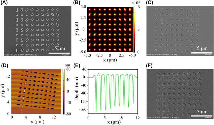
1644         Q. Jin et al.: Negative index metamaterial for photolithography

adjust the evanescent waves in more degrees of freedom                μ < 0, which then leads to a negative refractive index, n < 0.
[14–18], the overly short working distance (WD) and quite             The characteristics of plane waves in this medium can be
shallow pattern depth still obstruct the practical applica-           described by the wavevector k and the time average Poynting
tion of this exciting lithography scheme.                             vector S, which, respectively, give the directions of phase
     Interestingly, the negative index metamaterials (NIMs)           velocity Vp and energy flow, while, the direction of S could be
has been studied many years due to its inherent perfect               further represented by the direction of group velocity Vg in the
lens properties [19]. The light obeys Snell’s laws of refrac-         absence of loss. In this case, the medium, originally named
tion at the surface as light inside the NIMs, and forms a             ‘left-handed’ material, supports propagating solutions whose
negative angle with the surface normal. Then an image of              Vp and Vg are antiparallel. It means the signs of k and S are
light source would be shaped by refocusing light on the               opposite (k • S < 0) [28]. Unlike traditional materials, the NIMs
other side of the NIMs, which is predicted to obtain sub-             are often composited of noble metals (M) and dielectrics
wavelength focusing with resolution well below the                    (D) planar films in the visible and ultraviolet ranges [29–31].
diffraction limit. More importantly, the WD could be                  As shown in Figure 1A, the NIM structure is a stacked multi-
extended theoretically by increasing the thickness of the             layer, and each unit cell has an MD layer sequence. The ar-
NIM [20]. Although there is no material with both negative            rows depict the directions of k and S, performing negative
permittivity and permeability in nature, the negative                 refraction and backwards phase propagation. However, such
refractive index could be realized in microwave or even               NIM is generally regarded as a purely two-dimensional
infrared regions by constructing artificial metamaterials              isotropic, in other words, the negative refractive only could be
[20, 21]. However, it is difficult to achieve an acceptable            observed in-plane [24–27].
negative refractive index at ultraviolet frequency because                  To be used in photolithography, the negative refrac-
of substantial resonance losses and fabrication difficulties           tion need be extended to another dimension normal to the
[22, 23]. Interestingly, plasmonic waveguide-based meta-              plane of the NIM multilayers. Here, the proposed NIM
materials can achieve a negative refractive index at high             structure is consist of alternating Ag and TiO2 layers, which
frequencies [24, 25]. It is reported that the negative refrac-        are employed to form plasmonic waveguides stacked in the
tion at the dimension of perpendicular to the plane of the            z direction, and each unit cell has an MDMD layer sequence
layers could be achieved by employing strongly coupled                (40, 19, 45, and 19 nm, respectively). The individual film
plasmonic waveguides with symmetric modes [26, 27].                   thicknesses are optimized to achieve left-handed response
However, the excessive loss from the thick metal makes it             and admissible transmittance in the ultraviolet band
not suitable for subwavelength photolithography.                      (Supplementary Materials S1). It is worth noting that the
     Herein, we propose a subwavelength photolithog-                  transmittance could be enhanced by employing a material
raphy design by introducing a special NIM, which is con-              with low absorbtion, e.g. HfO2 (n ≈ 2.2) [32]. However, the
structed with stacked plasmonic waveguides but perform                NIM multilayer should be designed comprehensively. A
antisymmetric modes. Besides being achieved in-plane,                 dielectric with high refractive index and a metal with low
the negative refraction of both wavevector and energy flow            loss would present an NIM with attractive performance.
would be also achieved when an ultraviolet transverse                 Figure 1B gives the dispersion curves of the propagating
magnetic (TM)-polarized light incidents on the plane of the           modes in the designed plasmonic waveguides, which is
layers. The experimental results, along with numerical
                                                                      computed with transfer matrix method by using ϵm = 1 −
calculations, show that the air WD could be greatly
                                                                      ω2p /ω2 and εd = 8.52. The left-handed response acquires
improved in the exposure process, and the subwavelength
patterns could be produced in PR with well-shaped                     a negative Vg (i.e., dω/dk < 0), which is accomplished by
morphologies. Furthermore, arbitrary two-dimensional                  the plasmonic waveguide in a frequency range between
patterns over large area could be obtained by a single                the volume plasma frequency of the metal ωp and the sur-
exposure with a nonpolarized light. This NIM-based design             face plasmon frequency of the metal-dielectric inter-
presents a more practical method for improving sub-                   face (i.e., ωsp < ω < ωp). Hence, the k and S are
wavelength photolithography.                                          counterpropagating without considering the absorption,
                                                                      meaning the NIM can perform negative refraction in-plane. In
                                                                      addition, the waveguide supports antisymmetric mode
                                                                                                                        √̅̅̅̅̅̅̅̅̅̅
2 Principle and design                                                because of the dielectric thickness hd < ( πc/ωp ) (1 + ϵd )/ϵd
                                                                      [24], which is present by the magnetic field Hy in the inset.
Generally, NIMs are a kind of medium possess simultaneously           More importantly, this NIM also exhibit negative refraction
negative permittivity, ε < 0, and negative permeability,              when a TM-polarized light illuminates on the plane of the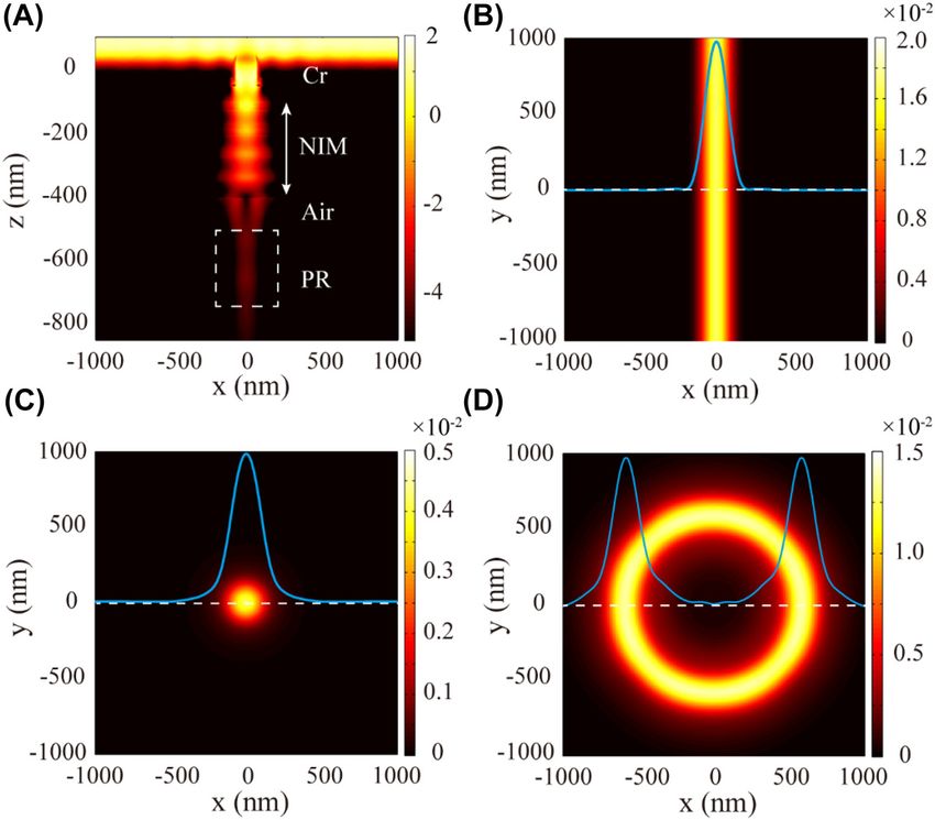
Q. Jin et al.: Negative index metamaterial for photolithography         1645

                                                                                        Figure 1: Design of a NIM for photolithography.
                                                                                        (A) Schematic of plasmonic waveguide-
                                                                                        based NIM multilayer. The dashed lines
                                                                                        indicate the incident plane of a TM-polarized
                                                                                        light parallels to the layers. Red and green–
                                                                                        blue arrows depict the directions of S and k,
                                                                                        respectively. (B) Dispersion relations for
                                                                                        modes in an MDM waveguide with hd = 19 nm
                                                                                        and εd = 8.52, where kp = ωp/c. The corre-
                                                                                        sponding structure and magnetic field dis-
                                                                                        tribution Hy along the z axis are shown in the
                                                                                        inset. (C) Schematic of the NIM-based
                                                                                        lithography design. (D) Three-dimensional
                                                                                        plots of EFCs for the plane wave with a
                                                                                        wavelength of 365 nm in NIM slab and in free
                                                                                        space. Si and St show the incident and
                                                                                        transmitted time-averaged Poynting vectors,
                                                                                        respectively; ki and kt give the incident and
                                                                                        transmitted wavevectors, respectively.

multilayers. It could be observed that the phase front in TM     would have a kt (pointing towards the interface) and a St
condition is refracted in a negative angle and propagated with   (pointing away from the interface) on the same side of the
a backward direction (Supplementary movies 1 and 2).             normal as the incident light, which is inferred from
Meanwhile, the direction of S inside the multilayer is anti-     the continuity of phase and conservation of energy [27].
parallel to the Vp, which is a signature of NIM. These fresh     The vivid description of phase fronts in this lithography
evidences state clearly that the proposed NIM with antisym-      system (normal incidence case) can be seen in Supple-
metric mode in waveguides could be used in subwavelength         mentary movie 3. It should be noted that kt and St are not
lithography.                                                     exactly collinear, which is mainly because the EFCs of the
     The diagram of the designed photolithography system         NIM is not a perfect sphere.
is shown in Figure 1C. A plane wave radiated from a mer-              Basically, the NIM multilayer could be considered as
cury lamp (i-line) normally incidents on the Cr mask from        an equivalent negative refractive slab. To give a visualized
the top side. The slots of the mask are flatted by coating        parametric analysis and confirm the validity of negative
poly(methyl methacrylate) (PMMA), which also works as            index for the proposed NIM, we perform a parameter
an index-matching layer [10, 15, 33]. The NIM multilayer         retrieval procedure using the commercial software FDTD
includes two MDMD layered unit cells and an additional Ag        solutions 2019. The NIM multilayer in air environment is
coupling layer. The waves transmitted through the multi-         normally illuminated by a broadband plane wave source
layer and 100 nm-thick air WD are regathered into the PR,        with the wavelength ranging from 300 nm to 400 nm. After
which is supported by another substrate.                         the steady state field distributions is obtained, the complex
     To illustrate the features of the NIM more clearly, the     reflection r and transmission t coefficients are calculated by
three-dimensional equi-frequency contours (EFCs) are             taking the ratios r = Er/E0 and t = Et/E0, where E0 is the
calculated by using εm = −2.26 + 0.46i and εd = 8.52 + 0.31i     complex electric field amplitude of the incident light, Er
(Figure 1D). The EFCs map the angular dependence of the          and Et are the reflected and transmitted complex electric
wavevector in the NIM and indicate the direction of the S        field amplitudes, respectively. Then, r and t could be
(which is normal to the EFCs and points in the direction of      related to the effective relative impedance Zeff and index
its displacement as a function of frequency). It can be seen     neff by using standard inverted reflection and transmission
that the EFCs of the NIM resemble a sphere with a radius of      parameter equations [34]. The effective relative permittivity
approximately k0. The wavevector magnitude decreases for         εeff and permeability μeff are calculated through the re-
increasing frequency, indicating that the Vg is oriented         lations ε = n/Z and μ = nZ. Figure 2 shows the resulting
inwards. The red arrow confirms that the S is directed in-        curves corresponding to the effective relative Zeff, neff, εeff,
wards (i.e., k • S < 0). For a plane wave incident from mask     and μeff of the NIM multilayer. It can be seen that the real
onto the surface of NIM, the transmitted backwards wave          part of the extracted neff is negative over the entire spectral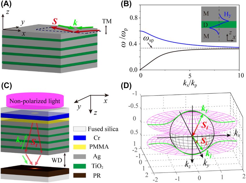
1646          Q. Jin et al.: Negative index metamaterial for photolithography

region. Specially, the real part of the neff is about −1.35 at         through the air WD. Because the realistic dispersion, loss
the wavelength of 365 nm. Meanwhile, it shows a double-                would result in the NIM never meet the idealized conditions
negative index composed of simultaneously negative real                [39], the diffracted waves are refocused at different posi-
parts of the permittivity and permeability. Therefore, the             tions. Finally, a pattern is formed in the following PR layer
proposed NIM not only performs negative refraction                     (εPR = 2.59) [33] with a depth over 200 nm. The cross section
[35, 36], but also exhibits a true negative refractive index           taken from the middle position of PR layer shows the full
characterized by negative refraction and backwards phase               width at half maximum (FWHM) of the straight line is
propagation. These parameters are extremely consistent                 ∼170 nm (Figure 3B).
with the definition of NIM [37]. If the NIM multilayer is                    Then, the masks changed into an isolated aperture
consider as an isotropic medium with neff = −1.35, the                 with a diameter of 180 nm. Notably, to obtain standard
direction of light could be observed intuitively with ray-             two-dimensional patterns and imitate a nonpolarized
tracing method (Supplementary material S2). On the other               light used in following experiments, the mask is illumi-
hand, when a plane wave in free space with an incident                 nated by superposing two incoherent linearly polarized
angle θi passing through the boundary between air and                  lights with vertical polarization. The normalized intensity
NIM, the neff also could be estimated qualitatively by using           distribution in PR shows a round dot with an FWHM of
Snell’s law, i.e., neff = sinθi/sinθr, where θr is the refraction      ∼220 nm (Figure 3C). The size expansion is mainly due to
angle of S inside the NIM. In our case, the calculated neff of         the adverse effect of TE-polarized components in hybrid
the NIM is about −1.31 (Supplementary material S3), in                 lighting (Supplementary materials S4), which also can be
agreement with the value derived from the parameter                    seen in the annular slit mask case shown in Figure 3D. It
retrieval procedure.                                                   presents that the annular slit with an outer diameter of
     To verify the foregoing analysis, several typical mask            700 nm and an inner diameter of 500 nm is regularly
patterns are employed to demonstrate the capability of the             imaged into the PR with an FWHM of ∼220 nm. Remark-
proposed photolithography system. Firstly, a straight slit             ably, the optical fields in PR have no any sidelobe or
with a width of 160 nm is prepared on the mask layer                   diffraction fringe, meaning the patterns could be pro-
(εCr = −8.62 + 9.23i) [38]. The normalized intensity distri-           duced with high fidelity, which is highly desirable in
bution in x–z plane is given in Figure 3A. Obviously, when             lithography. Admittedly, two-dimensional patterns also
the mask is irradiated by a TM-polarized light with a                  could be generated by illuminating with circularly
wavelength of 365 nm, the diffraction waves could be                   polarized light [14, 40]. However, the nonpolarized lights
excited and propagated efficiently in the NIM with negative             radiated from a mercury lamp has apparent advantages in
refraction angles, which then are refocused after passing              respect to convenience and robustness.

                                                                                            Figure 2: Effective parameters for the
                                                                                            designed NIM in the wavelength range of
                                                                                            300–400 nm.
                                                                                            (A–D) Corresponding real (′) and imaginary
                                                                                            (″) parts of the retrieved effective relative
                                                                                            impedance Zeff, index neff, permittivity εeff,
                                                                                            and permeability μeff.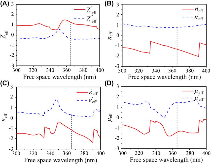
Q. Jin et al.: Negative index metamaterial for photolithography         1647

                                                                                            Figure 3: Simulated results of the NIM-based
                                                                                            lithography.
                                                                                            (A) Cross section of normalized intensity
                                                                                            distribution in logarithm scale inside the
                                                                                            NIM-based lithography design. (B–D)
                                                                                            Normalized intensity distributions in x–y
                                                                                            plane extracted from the middle position of
                                                                                            PR. The corresponding mask patterns are
                                                                                            straight slit, isolated aperture, and annular
                                                                                            slit, respectively. The insets show the related
                                                                                            intensity distributions along the dashed
                                                                                            lines.

3 Fabrication and lithography                                         column are related to the straight slit condition. Figure 5A
                                                                      is a scanning electron microscopy (SEM) image of the
  results                                                             mask. As expected, after transmitted through the NIM
                                                                      multilayer and air WD, the waves generate an identical
The key fabrication and exposure processes of the                     pattern in PR but the width is ∼180 nm (Figure 5D), which
NIM-based lithography is shown in Figure 4. Crucially, the            is close to the simulated result in Figure 3A. The difference
mask is flatted by the PMMA, which give a planar surface               could be ascribed to the broadband emission from
for depositing the NIM multilayers. The 100 nm-thick air              the mercury lamp (Supplementary Materials S5). The
WD is realized by fabricating a sunken step on the PR                 morphology of the pattern is measured by atomic force
substrate around the patterning areas. More importantly,              microscopy (AFM) and shown in Figure 5G. Clearly, the
the nonpolarized light radiated from a high pressure mer-             depth of the pattern exceeds 120 nm, which surpasses
cury lamp is used directly for exposure. All the patterns are         almost all reported results based on plasmonic lithography
produced with a single exposure process. The relevant                 [14, 40, 41]. More importantly, the neat patterning area
details are described in the Experimental Section.                    shows no diffraction fringe around the slit. Same perfor-
    Figure 5 shows the experimental results of the afore-             mances can also be seen in another two mask cases (cor-
mentioned three different masks. The pictures in left                 responding pictures in Figure 5B, E, H and Figure 5C, F, I),

Figure 4: Schematic diagrams for the processes of sample fabrication and lithography.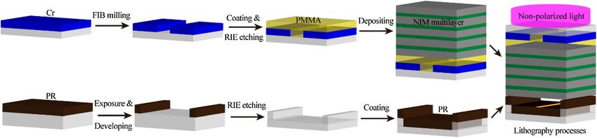
1648           Q. Jin et al.: Negative index metamaterial for photolithography

Figure 5: Experimental results of typical mask patterns in lithography with/without NIM multilayer.
(A–C) SEM images of the masks with a straight slit, isolated aperture, and annular slit, respectively. (D–F) Corresponding SEM images of the
patterns formed in PR. (G–I) Corresponding AFM images of the PR patterns. The insets present the depth profiles along the dashed lines. (J–L)
Corresponding SEM images of the PR patterns in control experiments.

where both the isolated aperture and annular slit are suc-               enhanced significantly, resulting in less exposure time.
cessfully imaged into PR with well-shaped morphologies.                  However, the light beams would diverge greatly as the
The widths of the two patterns in PR are ∼230 nm, and the                propagating distance increases. The patterns in PR are
depths reach 160 nm. Actually, if the adverse effect of                  expanded accordingly (Supplementary Materials S6). As
TE-polarized components is eliminated by illuminating                    observed in Figure 5J–L, the widths of the straight slit,
with a radially polarized beam, and using a light source                 isolated aperture, and annular slit are 345, 308, and
with narrow wavelength band, the FWHM of a circular or                   267 nm, respectively, which are much larger than the
annular pattern could be dramatically shrunk [42].                       NIM-based results. The rough edges and tiny ring in the
    The control experiments are also carried out. Without                central of the annular slit proves that unwanted in-
the NIM multilayer, the light intensity in PR could be                   terferences are happened during the imaging process.
Q. Jin et al.: Negative index metamaterial for photolithography 1649
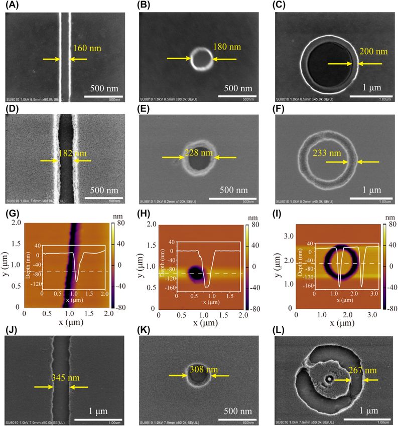
Figure 6: Experimental results of a mask with patterns over large area.
(A) SEM image of a mask constructed with aperiodic rectangles. (B) Normalized intensity distributions extracted from the position of 100 nm-
depth PR. (C, D) SEM and AFM images of the pattern formed in PR. (E) Corresponding depth profile along the dashed line in (D). (F) SEM images
of the PR patterns in control experiment.
The proposed subwavelength lithography system can 4 Conclusions
also fabricate arbitrary patterns over large area with a
single exposure process. As illustrative examples, typical In conclusion, an NIM is designed based on alternating
optical metasurface structures [43–45] are used to Ag/TiO2 multilayer with antisymmetric waveguide mode. It
demonstrate an economical and effective method in is proved that the negative refraction of both wavevector
fabrication. Figure 6A shows an SEM image of rectangles and energy flow can be realized when a TM-polarized light
array mask. The widths of all rectangles are 400 nm, while incident on the plane of the layers. Furthermore, the NIM
the lengths vary from 400 nm to 800 nm. Benefited from could be introduced into subwavelength photolithography
negative refraction of the NIM, the waves diffracted from to extend the WD and produce well-shaped arbitrary pat-
the mask could be regathered and produce well-shaped terns over large area. In the case of 100 nm-thick air WD,
patterns in PR (Figure 6B–E). The patterns with neat mor- subwavelength patterns with a depth reach 160 nm could
phologies indicates the disordered diffraction and intersect be obtained by illuminating with a mercury lamp. This
interference maybe not happened or affect the imaging strategy gives new insights into nanofabrication. The
process (more results in subwavelength sizes can be seen principle is also meaningful for studying optical imaging,
in Supplementary materials S7). Whereas the morphol- reversed Doppler effect, compact on-chip devices, etc.
ogies of the patterns in the control experiments present
obvious distortions (Figure 6F). Same performances can be
seen in the conditions of annular slits arrays and V-shaped
antennas (Supplementary material S8 and S9). Regret- 5 Experimental section
tably, the phenomena of corner rounding can be seen in the
First of all, a fused silica substrate is boiled in H2SO4:H2O2 (3:1) solu-
results of NIM-based lithography, which reveals it still
tion and ultrasonic cleaned in acetone and deionized water succes-
suffers from the optical proximity effect. However, this sively. The Cr film with a thickness of 60 nm is deposited on the
problem could be resolved distinctly by combining the substrate by Magnetron Sputtering (DE500, TE technology) with a
technology of optical proximity correct [46]. power of 400 W in radio frequency mode. The deposition rate is1650 Q. Jin et al.: Negative index metamaterial for photolithography
0.5 nm/s at a base pressure of 6.0 × 10⁻⁵ Pa. The mask patterns used in [2] L. Suslik, D. Pudis, J. Skriniarova, I. Martincek, I. Kubicova, and
this work are milled on the Cr film by Focused Ion Beam (Helios J. Kovac, “2D photonic structures for optoelectronic devices
Nanolab 650, FEI Company, @30 kV accelerating voltage). A PMMA prepared by interference lithography,” Phys. Procedia, vol. 32,
layer with a thickness of 80 nm is spin-coated on top of Cr mask and pp. 807–813, 2012.
baked for two and a half hours at 120 °C. Then, the PMMA layer is [3] M. H. Wu, C. Park, and G. M. Whitesides, “Fabrication of arrays of
etched by reactive ion etching with O2 to get a planar surface, and the microlenses with controlled profiles using gray-scale microlens
remained thickness is about 28 nm. The 9 layers of Ag/TiO2 multilayer projection photolithography,” Langmuir, vol. 18, pp. 9312–9318,
are alternatively deposited on the PMMA surface by magnetron sput- 2009.
tering without breaking vacuum. The optimized sputtering conditions [4] T. Ito and S. Okazaki, “Pushing the limits of lithography,” Nature,
include an Ar gas flow rate of 8 sccm, a base pressure of 5.0 × 10⁻⁵ Pa, vol. 406, pp. 1027–1031, 2000.
a power of 200 W in radio frequency mode for TiO2 and 100 W in [5] B. Buchegger, J. Kreutzer, B. Plochberger, et al., “Stimulated
direct current mode for Ag. The deposition rates for Ag and TiO2 emission depletion lithography with mercapto-functional
are 0.56 nm/s and 0.042 nm/s, respectively. The permittivities of Ag polymers,” ACS Nano, vol. 10, pp. 1954–1959, 2016.
and TiO2 used in main text are measured by Ellipsometer (SE 850, [6] R. Menon and H. I. Smith, “Absorbance-modulation optical
SENTECH). lithography,” J. Opt. Soc. Am. A, vol. 23, pp. 2290–2294, 2006.
In addition, the air WD is realized by fabricating a sunken step on [7] L. Qin, Y. Huang, F. Xia, et al., “5 nm nanogap electrodes and
the PR substrate around the patterning area. Firstly, the AR-3100 arrays by super-resolution laser lithography,” Nano Lett., vol. 20,
positive PR (ALLRESIST GmbH, Strausberg) with a thickness of pp. 4916–4923, 2020.
∼1000 nm is spin-coated onto a substrate and baked for 5 min at [8] M. M. Alkaisi, R. J. Blaikie, S. J. McNab, R. Cheung, and
100 °C. A sunken step with a diameter over 10 mm is fabricated by D. R. S. Cumming, “Sub-diffraction-limited patterning using
traditional photolithography. Then the step is transferred to the sub- evanescent near-field optical lithography,” Appl. Phys. Lett.,
strate by reactive ion etching with CH3F3. And the etching depth is vol. 75, pp. 3560–3562, 1999.
∼100 nm. The acetone is used to remove the residual PR. At last, The [9] F. Hong and R. Blaikie, “Plasmonic lithography: recent
AR-P 3170 positive PR is spin-coated onto the substrate and baked for progress,” Adv. Opt. Mater., vol. 3, p. 1801653, 2019.
5 min at 100 °C. The PR thickness at the sunken step area is ∼160 nm [10] N. Fang, H. Lee, S. Cheng, and X. Zhang, “Sub-diffraction-limited
measured by a surface profiler. optical imaging with a silver superlens,” Science, vol. 308,
In the exposure process, the PR/substrate is in conformal contact pp. 534–537, 2005.
with NIM/mask/substrate with the aid of air pressure (∼0.8 MPa). All [11] W. Srituravanich, L. Pan, Y. Wang, et al., “Flying plasmonic lens
the masks are normally illuminated by a nonpolarized light with a in the near field for high-speed nanolithography,” Nat.
central wavelength of 365 nm (i-line) radiated from a mercury lamp. Nanotechnol., vol. 3, pp. 733–737, 2008.
The exposure intensity and time are set to be 0.22 mW/cm2 and 300– [12] J. Ji, Y. Meng, Y. Hu, et al., “High-speed near-field
400 s, respectively. Then, the PR layer is developed for 20 s in a mixed photolithography at 16.85 nm linewidth with linearly polarized
solution of AR 300–35 and deionized water with a volume ratio of 1:1, illumination,” Opt. Express, vol. 25, pp. 17571–17580, 2017.
rinsed with deionized water and dried by N2 gas in order. [13] Y. Hu, L. Li, R. Wang, et al., “High-speed parallel plasmonic
direct-writing nanolithography using metasurface-based
Acknowledgments: The authors thank Kaipeng Liu, plasmonic lens,” Engineering, vol. 7, pp. 1623–1630, 2021.
[14] G. Liang, C. Wang, Z. Zhao, et al., “Squeezing bulk plasmon
Guoping Liu for the helpful advises in experiment, and
polaritons through hyperbolic metamaterials for large area deep
thank Yunfei Luo, Ping Gao, Zubo Cai for the technical subwavelength interference lithography,” Adv. Opt. Mater.,
supports in FIB lithography and SEM detection. vol. 3, pp. 1248–1256, 2015.
Author contribution: All the authors have accepted [15] X. Chen, F. Yang, C. Zhang, J. Zhou, and L. J. Guo, “Large-area
responsibility for the entire content of this submitted high aspect ratio plasmonic interference lithography utilizing a
single high-k mode,” ACS Nano, vol. 10, pp. 4039–4045, 2016.
manuscript and approved submission.
[16] M. Lee, E. Lee, S. So, et al., “Bulk metamaterials exhibiting
Research funding: This work was supported by National chemically tunable hyperbolic responses,” J. Am. Chem. Soc.,
Natural Science Foundation of China (61905032, 61927818, vol. 143, pp. 20725–20734, 2021.
62005288), Natural Science Foundation of Chongqing [17] D. Lee, S. So, G. Hu, et al., “Hyperbolic metamaterials: fusing
(cstc2020jcyj-msxmX0428), and Fundamental Research artificial structures to natural 2D materials,” eLight, vol. 2,
Funds for the Central Universities (2020CDJQY-A029, pp. 1–23, 2022.
[18] G. Liang, X. Chen, Q. Zhao, et al., “Achieving pattern uniformity in
2020CDJLHZZ-072).
plasmonic lithography by spatial frequency selection,”
Conflict of interest statement: The authors declare no Nanophotonics, vol. 7, pp. 277–286, 2018.
conflicts of interest regarding this article. [19] J. B. Pendry, “Negative refraction makes a perfect lens,” Phys.
Rev. Lett., vol. 85, pp. 3966–3969, 2000.
[20] D. R. Smith, J. B. Pendry, and M. C. K. Wiltshire, “Metamaterials
and negative refractive index,” Science, vol. 305, pp. 788–792,
References 2004.
[21] C. M. Soukoulis, S. Linden, and M. Wegener, “Negative refractive
[1] J. H. Bruning, “Optical lithography: 40 years and holding,” Proc. index at optical wavelengths,” Science, vol. 315, pp. 47–49,
SPIE-Opt., vol. 6520, p. 652004, 2007. 2007.Q. Jin et al.: Negative index metamaterial for photolithography 1651
[22] G. Doling, M. Wegener, C. M. Soukoulis, and S. Linden, visible frequencies,” Nat. Mater., vol. 9, pp. 407–412,
“Negative-index metamaterial at 780 nm wavelength,” Opt. Lett., 2010.
vol. 32, pp. 53–55, 2007. [35] A. J. Hoffman, L. Alekseyev, S. S. Howard, et al., “Negative
[23] V. G. Veselago and E. E. Narimanov, “The left hand of brightness: refraction in semiconductor metamaterials,” Nat. Mater., vol. 6,
past, present and future of negative index materials,” Nat. pp. 946–950, 2007.
Mater., vol. 5, pp. 759–762, 2006. [36] Y. Liu, G. Bartal, and X. Zhang, “All-angle negative refraction and
[24] X. Fan, G. P. Wang, J. C. Lee, and C. T. Chan, “All-angle broadband imaging in a bulk medium made of metallic nanowires in the
negative refraction of metal waveguide arrays in the visible visible region,” Opt. Express, vol. 16, pp. 15439–15448, 2008.
range: theoretical analysis and numerical demonstration,” Phys. [37] V. G. Veselago, “The electrodynamics of substances with
Rev. Lett., vol. 97, p. 073901, 2006. simultaneously negative values of ε and μ,” Phys. Usp., vol. 10,
[25] J. A. Dionne, E. Verhagen, A. Polman, and H. A. Atwater, “Are pp. 509–514, 1968.
negative index materials achievable with surface plasmon [38] E. D. Palik, Handbook of Optical Constants of Solids, San Diego,
waveguides? A case study of three plasmonic geometries,” Opt. CA, Academic Press, 1985, pp. 374–385.
Express, vol. 16, pp. 19001–19017, 2008. [39] R. W. Ziolkowski and E. Heyman, “Wave propagation in media
[26] E. Verhagen, R. de Waele, L. Kuipers, and A. Polman, “Three- having negative permittivity and permeability,” Phys. Rev. E,
dimensional negative index of refraction at optical frequencies vol. 64, p. 056625, 2001.
by coupling plasmonic waveguides,” Phys. Rev. Lett., vol. 105, [40] L. Liu, P. Gao, K. Liu, et al., “Nanofocusing of circularly polarized
p. 223901, 2010. Bessel-type plasmon polaritons with hyperbolic
[27] T. Xu, A. Agrawal, M. Abashin, K. J. Chau, and H. J. Lezec, metamaterials,” Mater. Horiz., vol. 4, pp. 290–296, 2017.
“All-angle negative refraction and active flat lensing of [41] X. Luo and T. Ishihara, “Surface plasmon resonant interference
ultraviolet light,” Nature, vol. 497, pp. 470–474, 2013. nanolithography technique,” Appl. Phys. Lett., vol. 84,
[28] C. M. Soukoulis and M. Wegener, “Past achievements and future pp. 4780–4782, 2004.
challenges in the development of three-dimensional photonic [42] Q. Jin, G. Liang, G. Chen, et al., “Enlarging focal depth using
metamaterials,” Nat. Photonics, vol. 5, pp. 523–530, 2011. epsilon-near-zero metamaterial for plasmonic lithography,” Opt.
[29] H. Cho, Y. Yang, D. Lee, et al., “Experimental demonstration of Lett., vol. 45, pp. 3159–3162, 2020.
broadband negative refraction at visible frequencies by critical [43] J. Gao, S. Yan, Y. Zhou, et al., “Polarization-conversion
layer thickness analysis in a vertical hyperbolic metamaterial,” microscopy for imaging the vectorial polarization distribution in
Nanophotonics, vol. 10, pp. 3871–3877, 2021. focused light,” Optica, vol. 8, pp. 984–994, 2021.
[30] H. Cho, S. So, T. Badloe, et al., “Critical layer thickness analysis [44] Y. Wang, Q. Fan, and T. Xu, “Design of high efficiency achromatic
of vertically stacked hyperbolic metamaterials for effective metalens with large operation bandwidth using bilayer
negative refraction generation,” Adv. Theor. Simul., vol. 3, architecture,” Opto-Electron. Adv., vol. 4,
p. 2000138, 2020. pp. 20000801–20000815, 2021.
[31] S. Bang, S. So, and J. Rho, “Realization of broadband negative [45] N. Yu, P. Genevet, M. A. Kats, et al., “Light propagation with
refraction in visible range using vertically stacked hyperbolic phase discontinuities: generalized laws of reflection and
metamaterials,” Sci. Rep., vol. 9, pp. 1–7, 2019. refraction,” Science, vol. 334, pp. 333–337, 2011.
[32] C. Zhang, S. Divitt, Q. Fan, et al., “Low-loss metasurface optics [46] G. Chen, S. Li, and X. Wang, “Efficient optical proximity
down to the deep ultraviolet region,” Light Sci. Appl., vol. 9, correction based on virtual edge and mask pixelation with
pp. 1–10, 2020. two-phase sampling,” Opt. Express, vol. 29, pp. 17440–17463,
[33] X. Chen, C. Zhang, F. Yang, et al., “Plasmonic lithography 2021.
utilizing epsilon near zero hyperbolic metamaterial,” ACS Nano,
vol. 11, pp. 9863–9868, 2017.
[34] S. P. Burgos, R. de Waele, A. Polman, and H. A. Atwater, Supplementary Material: The online version of this article offers sup-
“A single-layer wide-angle negative-index metamaterial at plementary material (https://doi.org/10.1515/nanoph-2022-0013).You can also read