Metal halide perovskite light emitters - PNAS
←
→
Page content transcription
If your browser does not render page correctly, please read the page content below
S P E C I A L F E A T U R E:

                                                                               SPECIAL FEATURE: PERSPECTIVE
        PERSPECTIVE

                                                                          Metal halide perovskite light emitters
                                                                           Young-Hoon Kima,b,1, Himchan Choa,b,1, and Tae-Woo Leea,b,2

                                                                           Edited by John A. Rogers, University of Illinois, Urbana, IL, and approved August 16, 2016 (received for review May 10, 2016)

                                                                           Twenty years after layer-type metal halide perovskites were successfully developed, 3D metal halide
                                                                           perovskites (shortly, perovskites) were recently rediscovered and are attracting multidisciplinary interest
                                                                           from physicists, chemists, and material engineers. Perovskites have a crystal structure composed of five
                                                                           atoms per unit cell (ABX3) with cation A positioned at a corner, metal cation B at the center, and halide
                                                                           anion X at the center of six planes and unique optoelectronic properties determined by the crystal
                                                                           structure. Because of very narrow spectra (full width at half-maximum ≤20 nm), which are insensitive to
                                                                           the crystallite/grain/particle dimension and wide wavelength range (400 nm ≤ λ ≤ 780 nm), perovskites are
                                                                           expected to be promising high-color purity light emitters that overcome inherent problems of conventional
                                                                           organic and inorganic quantum dot emitters. Within the last 2 y, perovskites have already demonstrated
                                                                           their great potential in light-emitting diodes by showing high electroluminescence efficiency comparable to
                                                                           those of organic and quantum dot light-emitting diodes. This article reviews the progress of perovskite
                                                                           emitters in two directions of bulk perovskite polycrystalline films and perovskite nanoparticles, describes
                                                                           current challenges, and suggests future research directions for researchers to encourage them to collabo-
                                                                           rate and to make a synergetic effect in this rapidly emerging multidisciplinary field.
                                                                                                                   |                        |                     |               |
                                                                           organic–inorganic hybrid perovskite light-emitting diodes polycrystalline film nanoparticle vivid display

                                                                           As human civilization went through the information                     They were expected to be novel hybrid materials that
                                                                           revolution, display technology has been designated as a                had both advantages of organic materials (e.g., solu-
                                                                           core technology to increase convenience in daily human                 tion processability and low material costs) and inor-
                                                                           life. In an information society, the desire of humans to see           ganic materials (e.g., high charge carrier mobility) (7).
                                                                           the materials more vividly in displays has significantly               Especially, perovskites with high color purity, easy
                                                                           increased. In this aspect, major trend of the display                  wavelength tuning, and efficient charge injection/
                                                                           technology is changing from high resolution and high                   transport property have been intensively studied as
                                                                           efficiency to high color purity for realizing vivid natural            promising candidates for future light emitters (8–10).
                                                                           colors (Fig. 1). Therefore, research on new emitting mate-             Furthermore, stable and environmentally benign perov-
                                                                           rials that can emit light with narrow full width at half-              skites, which were recently reported, further raise the
                                                                           maximum (FWHM) have been attempted. Inorganic                          possibility of perovskites as future emitters in display
                                                                           quantum dot (QD) emitters with narrow spectra (FWHM                    technology (11–19).
                                                                           ∼30 nm) have been significantly studied following organic                  However, early works on layer-type (i.e., 2D) perovskite
                                                                           emitters (FWHM >40 nm); however, size-sensitive color                  emitters, in the 1990s, did not gain much attention (1–5).
                                                                           purity, difficult size uniformity control, and expensive ma-           The layer-type perovskite emitters incorporating long-
                                                                           terial costs of inorganic QD emitters retard the progress              chain organic ammoniums can generate stable excitons
                                                                           for wide use in industry. Therefore, new emitters with                 at low temperature, but the photoluminescence (PL) in-
                                                                           size-insensitively high color purity (FWHM
Fig. 1. Major trend of display technology. Data are taken from references as follows: OLEDs, refs. 30–41; QD LEDs, refs. 20–29; and PeLEDs, refs. 8–10.

                                          external quantum efficiency (EQEmax) of 0.11% (7). However, this emis-        relatively narrow (FWHM ∼30 nm) but size-sensitive spectra in lim-
                                          sion originated not from the inorganic frameworks but from the or-            ited dimension (≤10 nm) (Fig. 2C).
                                          ganic dye ligands; thus, PeLEDs showed very low color purity                      The polar lead–halide bonds in perovskite crystal induce the
                                          (FWHM ≥ 100 nm) compared with inorganic QD LEDs (20–29),                      Fröhlich interaction between charge carriers and longitudinal
                                          and inferior EL efficiency compared with organic LEDs (OLEDs)                 optical (LO) phonons, which results in LO phonon scattering and
                                          (30–41). As a result, the development of these perovskite emitters has        electron–phonon coupling; these predominantly determine the
                                          been retarded, whereas organic emitters and inorganic QD emitters             linewidth of emission spectrum (FWHM ∼20 nm) (44). Further-
                                          have been intensively studied for 27 y and 22 y, respectively (20–41).        more, the traps and impurities in perovskites, which can arise from
                                              In 2012, the first 3D perovskite emitters, CH3NH3PbBr3 nano-              the low crystallinity, do not make a significant effect on the FWHM
                                          particles (NPs) in porous alumina (42), were reported, and the pos-           because trap-assisted recombination is mostly nonradiative decay
                                          sibility of perovskites as emitters was rediscovered. As a result, since      and impurity-contributed linewidth broadening is negligible, re-
                                          2014, the research on 3D perovskite emitters has intensively grown            spectively (44, 45). Thus, perovskites showed the size-insensitive
                                          and focused on achieving high efficiency in PL and EL. Within the             FWHM, which is only affected by the crystal structure rather than
                                          last 2 y, more than 72 papers on perovskite emitters were published,          quality and dimension of perovskite crystal.
                                          and EQEmax of 8.53% and photoluminescence quantum efficiency                      In general, photoexcitation or charge carrier injection by external
                                          (PLQE) of more than 90% were reported (10, 43).                               field forms geminate electron–hole pairs, which can (i) be dissoci-
                                              In this Perspective, we highlight the potential of perovskites as         ated into free charge carriers or (ii) form excitons (46, 47). The Eb
                                          promising emitters that can be mainstream in the research field of            reflecting the strength with which geminate electron–hole pairs are
                                          displays and solid-state lightings. In addition, we present our               bound and the excitation density affecting the frequency with which
                                          perspectives on the progress of perovskite emitters in two direc-
                                          tions: bulk perovskite polycrystalline films (PePCs) and perovskite
                                          nanoparticles (PeNPs). Finally, we suggest future research directions
                                          of perovskite emitters that may engage a researcher’s attention in
                                          this research field.

                                          Fundamental Properties of Perovskite Emitters
                                          Three-dimensional perovskites have an ABX3 crystal structure com-
                                          posed of five atoms per unit cell, with cation A positioned at a
                                          corner, metal cation B at the center, and six nearest-neighbor anions
                                          X with octahedral corner sharing at the center of six planes (Fig. 2A).
                                          Generally, perovskites consist of organic ammonium (CnH2n+1NH3+)
                                          or organic amidinium [e.g., CH(NH2)+] or alkali metals such as Cs at
                                          the A site, divalent transition metals (e.g., Pb2+, Eu2+, Sn2+, Cu2+) at
                                          the B site, and halide anions (I−, Br−, Cl−) at the X site.
                                              Perovskite emitters show size-insensitively very narrow spectra
                                          (FWHM ∼20 nm) in wide wavelength range (400 nm ≤ λ ≤ 780 nm)
                                          according to their inherent crystal structure (Fig. 2B). Therefore,
                                          they can have a very wide color gamut in Commission Inter-
                                          nationale de l’Éclairage diagram. This highlights that perovskites
                                          can be promising emitters especially in display fields. On the other
                                                                                                                        Fig. 2. (A) Schematic of crystal structure, (B) schematic of emission
Downloaded by guest on October 14, 2021

                                          hand, organic emitters showed broad spectra (FWHM ≥40 nm)                     of metal halide perovskites, and (C) FWHM and dimension of
                                          in large dimension (≥10 nm) and inorganic QD emitters showed                  perovskite, inorganic QD, and organic emitters.

                                          Kim et al.                                                                                          PNAS | October 18, 2016 | vol. 113 | no. 42 | 11695
electrons and holes meet together determine the ratio of free car-         (EQEmax = 0.125% and Lmax = 417 cd·m−2) by using modified
                                          riers and excitons (nfc/ne-h, where nfc is the number of free carriers     interlayers (9). These works demonstrated that pure perovskites
                                          and ne-h is the number of geminate electron–hole pairs) (46). Many         can emit bright EL with very high color purity at RT. Many
                                          researchers have claimed that perovskites have Wannier-type exci-          subsequent studies used a variety of experimental approaches
                                          tons with low Eb (e.g., 76 or 150 meV for CH3NH3PbBr3) and high            to improve the luminescence efficiencies of PeLEDs (8–10,
                                          dielectric constant (46–48). Thus, at RT, most of Wannier excitons         49–66).
                                          dissociate into free carriers (nfc/ne-h ∼ 1) because there is almost no        In 2015, Lee and coworkers first showed the possibility of high-
                                          electron–hole wavefunction overlap and exciton–exciton interaction         efficiency PeLEDs (EQEmax = 8.53%) comparable to those of OLEDs
                                          (46). Charge trapping by trap states also induces the dissociation of      (10) (Fig. 3A and Table 1). These increases in EQE of PeLEDs re-
                                          excitons into free carriers and the nonradiative recombination             semble the dramatic increase in power conversion efficiency of pe-
                                          pathways of free carriers and excitons, and thereby limits the             rovskite solar cells and demonstrate the great potential of perovskite
                                          luminescence efficiency at low fluences (47).                              emitters. To increase the efficiency of PeLEDs, the origins of low
                                                However, high excitation density of >1020 cm−3 increases the         device efficiency were identified and many solutions were developed
                                          number of charge carriers and wavefunction overlap of them in              or suggested (8–10, 49–66). We categorize these approaches into (i)
                                          perovskites, fills the trap states, and thus leads to favorable exciton    use of interlayers and (ii) modification of perovskite layers.
                                          formation over dissociation into free carriers (nfc/ne-h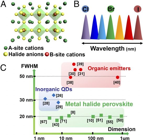
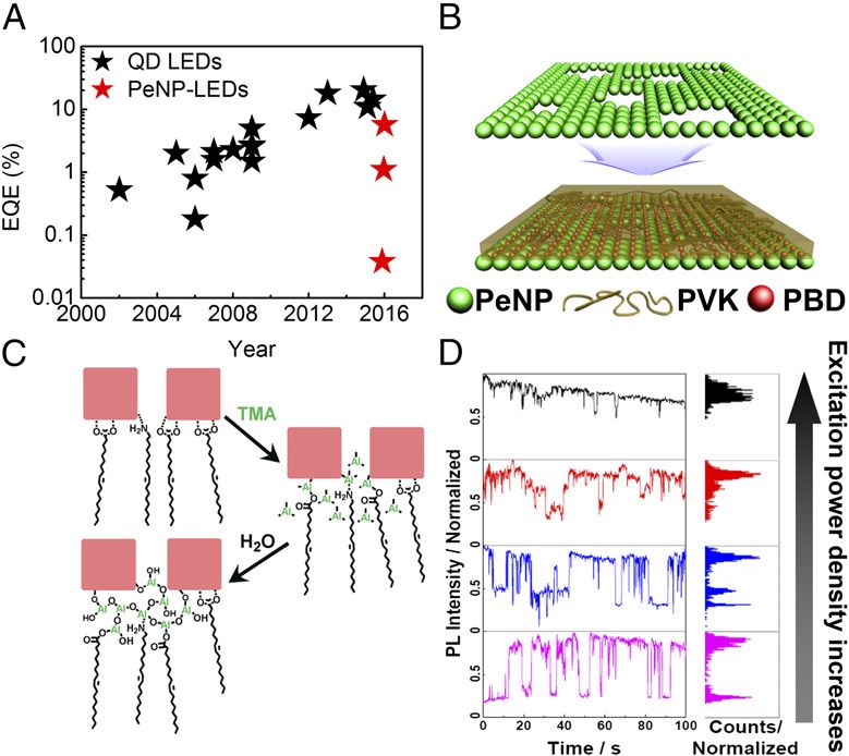
Table 1. Overview of reported results from PePC-based LEDs
Previous Publication Rmax,
reports (ref.) year/month Emission layer FWHM, nm CEmax, cd·A−1 W·sr−1·m−2 EQEmax, % Lmax, cd·m−2
Tan et al. (8) 2014/08 MAPbBr3 20 (green) 0.3 13.2 0.1 (green) 0.76 (IR) 364
MAPbI3 35 (IR)
Kim et al. (9) 2014/11 MAPbBr3 ∼20 0.577 n.r. 0.125 417
Hoye et al. (49) 2015/01 MAPbBr3 25 ∼0.27 n.r. n.r. 550
Kumawat et al. (50) 2015/01 MAPbBr3 (green) 30.9 (green) ∼1.8 × 10⁻² (green) 5 × 10⁻³ ∼6.5 × 10⁻³ (green) 20 (green)
MAPbI1.19Br1.37Cl0.44 (red) 40.6 (red) ∼2.8 × 10⁻⁴ (red) 0.28 (red) 0.26 (red)
MAPbI3-xCl3 (IR) 32.7 (IR) 0.18 (IR)
Li et al. (51) 2015/02 MAPbBr3 19 n.r. n.r. 1.2 ∼2,500
Wang et al. (52) 2015/02 MAPbBr3 22 (green) n.r. 28 ∼0.8 (green) ∼20,000
MAPbI3-xClx 37 (IR) 3.5 (IR)
Sadhanala et al. (53) 2015/02 MAPbI3-xClx ∼41 n.r. n.r. 0.024 —
Qin et al. (54) 2015/03 MAPbBr3 20 n.r. n.r. ∼0.1 ∼1,500
Yu et al. (55) 2015/05 MAPbBr3 41 0.22 n.r. 0.051 ∼545
Kumawat et al. (56) 2015/06 MAPbBr1.86Cl1.14 (green) ∼40 (green) ∼9 × 10⁻³ (green) n.r. ∼3 × 10⁻⁴ (blue) ∼1.2 (green)
MAPbBr1.08Cl1.92 (blue) ∼20 (blue) ∼3.5 × 10⁻⁴ (blue)
Yantara et al. (57) 2015/10 CsPbBr3 18 0.035 n.r. 0.008 407
Yu et al. (58) 2015/11 MAPbBr3 ∼20 0.43 n.r. 0.1 3,490
Cho et al. (10) 2015/12 MAPbBr3 ∼20 42.9 n.r. 8.53 16,936
Bade et al. (59) 2015/12 MAPbBr3 ∼20 4.91 n.r. 1.1 21,014
Bi et al. (63) 2016/01 FAPbI3 n.r. n.r. n.r. ∼0.5 n.r.
Shi et al. (60) 2016/03 MAPbBr3 30 0.12 n.r. 0.0645 196
Wang et al. (61) 2016/04 MAPbBr3 ∼25 n.r. n.r. 0.43 4,890
Byun et al. (65) 2016/06 (C6H5C2H4NH3)2MAm−1PbmBr3m+1 ∼20 4.9 n.r. n.r. 2935
Yuan et al. (66) 2016/06 (C6H5C2H4NH3)2MAn−1PbnBr3n+1 ∼50 n.r. 80 8.8 n.r.
m, 1–4, integer; n, integer; n.r., not reported.
to 5.95 eV (surface) (9). The rich PFI on the surface effectively film (10). In perovskite solar cells, the solvent dripping was designed
blocked exciton quenching at the interface between PEDOT:PSS: not for rapid pinning of crystal growth to achieve small grains but for
PFI and MAPbBr3 (9). With these strategies, the current efficiency making uniform PePCs with large grain size to facilitate the diffusion
CE of PeLEDs increased from 1.65 × 10⁻³ to 0.577 cd·A−1, and the and dissociation of excitons; however, the process cannot be ap-
luminance improved from 1.38 to 417 cd·m−2 (9). plied to PeLEDs because the grain size should be decreased to in-
Also, electron injection barriers from cathodes to perovskite layers crease the luminescence efficiencies of PePCs (10). Decreased grain
must be overcome in inverted structure PeLEDs. Hoye et al. (49) used size and increased area of grain boundary can spatially confine
spatial atmospheric atomic layer-deposited (SAALD) ZnO layers as excitons or charge carriers and block their diffusion, and, as a con-
electron transport layers instead of previously reported polyfluorene sequence, increase the radiative recombination. Therefore, it is
(8). The PeLEDs based on SAALD ZnO exhibited a very low turn-on necessary to develop an optimal solvent-dripping process that can
voltage Vturn-on = 2 V, and Lmax = 550 cd·m−2. Polyethyleneimine (PEI) fabricate PePCs with minimal grain size. Use of DMSO (which has a
interlayers decreased the electron affinity of ZnO layers from 3.7 to higher boiling point of 189 °C than DMF, which has boiling point of
3.2 eV, and thereby made ohmic electron injection into perovskite 153 °C) as a solvent can delay spontaneous crystallization of pe-
layers possible (52). Furthermore, the hydrophilic surface of PEI-treated rovskites and thereby facilitate the optimization of solvent-dripping
process (10). Also, the perovskite’s crystallization behavior and the
ZnO layers improved the uniformity of perovskite layers. With these
final film morphology depend on the physical properties of dripping
modifications, MAPbBr3 PeLEDs exhibited very high Lmax of ∼20,000
solvents (68). Therefore, the choice of dripping solvents to fabricate
cd·m−2 and EQEmax of 0.8%, and MAPbI3-xClx infrared PeLEDs
perovskite films most suitable for PeLEDs is an important task.
exhibited Rmax of ∼28 W sr−1·m−2 and EQEmax of 3.5%, respectively
Dripping of chloroform, a highly volatile solvent (boiling point, 61.2 °C),
(52). These dramatically increased EQEmax compared with previous
on the growing quasifilm during spin-coating of MAPbBr3/DMSO
works (8, 9, 49, 50) are possibly due to the well-optimized film mor-
with the optimized dripping conditions resulted in small MAPbBr3
phology of perovskite layers and reduced charge injection barriers.
grains (100–250 nm) possibly because of minimized crystal growth
time after supersaturation (10). This process was called as “nano-
Modification of Perovskite Layers. Uniform morphology of pe- crystal pinning” (NCP).
rovskite layers can also be achieved by modifying the process by The NCP by a volatile polar solvent (S-NCP) was modified to
which perovskite layers are formed. Spontaneous crystallization of further decrease the grain size. Additive-based NCP (A-NCP), in
perovskites by spin-coating often causes nonuniform and discon- which organic small molecules 2,2′,2″-(1,3,5-benzinetriyl)-tris(1-
tinuous film with scattered perovskite crystals (10). An effective phenyl-1-H-benzimidazole) (TPBI) were included in the dripping
method to overcome this nonuniformity is to use nonpolar solvent solvent (chloroform), effectively inhibited growth of MAPbBr3 crys-
dripping (10, 67). By dripping nonpolar solvents (e.g., chloroform, tals and substantially reduced MAPbBr3 average grain size to
chlorobenzene, toluene) that do not dissolve perovskite precursors 99.7 nm. PeLEDs based on A-NCP exhibited significantly high EQEmax
onto the wet perovskite films during spin-coating, aprotic polar of 8.53% and maximum CE of 42.9 cd·A−1 (10).
solvents [e.g., dimethylformamide (DMF), dimethyl sulfoxide Another method to create uniform film morphology is to
Downloaded by guest on October 14, 2021
(DMSO), and γ-butyrolactone] can be washed away and immediate control the solubility of perovskite precursors and crystallization
crystallization of perovskites occurs; the result is a uniform and dense rate of perovskites (58). HBr incorporation into MAPbBr3/DMF
Kim et al. PNAS | October 18, 2016 | vol. 113 | no. 42 | 11697solutions increased the solubility of MAPbBr3 and decreased the be used in LEDs because they need a nanoporous hard template
crystallization rate; the HBr concomitantly increased supersatura- such as Al2O3 or TiO2 (42, 75). For application to LEDs and other
tion concentration and reduced the final film thickness; uniform optoelectronics, colloidal NPs synthesized by solution reaction
and continuous MAPbBr3 films resulted (58). Using this approach were demonstrated. The first colloidal PeNPs were synthesized
with optimized HBr concentration (6 vol%), bright PeLEDs with by “nontemplate” (NT) methods, which can synthesize mono-
EQEmax of 0.1% and Lmax of 3,490 cd·m−2 were achieved (58). dispersed PeNPs in solution (69). The authors formed colloidal
To fill the voids in perovskite crystals, an insulating polymer, PeNPs by adding MA bromide (MABr) and PbBr2 into a mixture of
polyimide precursor (PIP), was mixed in perovskite solutions (51). oleic acid, octadecene, and long-chain alkyl ammonium bromide
The presence of PIP between the scattered MAPbBr3 crystals as a ligand, at 80 °C. The first PeNPs synthesized by NT methods
blocked the flow of leakage current, which caused significant re- showed PLQE of 20% and good dispersability in various protic
duction in EL efficiency. The composite film was optimized at solvents (69). PLQE was increased to 83% by finely tuning the
the ratio of MAPbBr3:PIP = 1:1 (wt/wt), and the corresponding molar ratio of MABr, PbBr2, and ligands (70).
PeLEDs showed EQEmax of 1.2% (51). Recently, Kovalenko and coworkers (43) reported all-inorganic
Although a uniform morphology can be achieved by using metal halide PeNPs, CsPbX3 (X = Cl, Br, I) that showed PLQE of
various strategies described above, the luminescent property of >90%, high color purity (12 ≤ FWHM ≤ 42 nm), wide color tunability
perovskite films can be further improved by controlling the pre- of 410–700 nm, and wide color gamut of 140% of the National
cursor ratio (10, 57). The use of MABr-rich MAPbBr3 solutions Television System Committee color standard. The PeNPs were
resulted in significantly enhanced EQE and luminance, because synthesized using the “hot-injection” (HI) method, in which the
slightly excess MABr made well-matching stoichiometry and pre- Cs-oleate is injected into a mixture of oleic acid, oleylamine, and
vented the formation of metallic Pb atoms that strongly quench PbX2 in octadecene solution at a temperature of >140 °C. The
luminescence (10). The precursor ratio, MABr:PbBr2, was optimized emission color and size can be controlled by adjusting reaction time
at 1.05:1 (mol:mol) because the insulating nature of more excess and temperature (43, 76, 77). This method imitates the synthesis
MABr can block efficient charge transport. Using the optimized route of colloidal chalcogenide QDs such as CdSe QDs, but is much
precursor ratio of MABr:PbBr2 of 1.05:1, >100 times higher CE (21.4 simpler than those of colloidal inorganic QDs because PeNPs do not
cd·A−1) was obtained than that of the device with equimolar pre- need complex surface passivation process (20–29). However, HI
cursor ratio (0.183 cd·A−1) (10). The control of precursor ratio is also methods still use toxic and unstable organic solvents, and must be
useful in the all-inorganic perovskite CsPbBr3 (57). conducted in a nitrogen environment at high temperature (>140 °C),
The use of quasi-2D perovskite structures can also be a useful so the prospects of commercialization may be limited (43, 76–78).
strategy to increase the efficiency of PeLEDs (65, 66). Very recently, Recently, Zhang et al. (71) reported MAPbBr3-based PeNPs
high-efficiency quasi-2D PeLEDs based on MA-phenylethyl am- synthesized at RT, which had PLQE of >70%, good color purity, and
monium (PEA) mixed cations were reported (65, 66). The optimized color tunability. All-inorganic PeNPs (CsPbX3) can also be synthe-
MA:PEA ratio led to the improved uniformity of perovskite film, strong sized by the same process with MAPbBr3 PeNPs synthesized at RT
exciton confinement, and the decrease in trap density, resulting in (78). The authors synthesized colloidal NPs by dropping a perovskite
high-efficiency green PeLEDs (CEmax = 4.90 cd·A−1) (65). The highly precursor solution in a good solvent (e.g., DMF) to a bad solvent
efficient infrared PeLEDs (EQEmax = 8.8%) based on the quasi-2D (e.g., toluene) under vigorous stirring. Due to poor solubility of pe-
perovskite structure (PEA2(MA)n−1PbnI3n+1) were shown with the sys- rovskites in a bad solvent, they recrystallized when they met the
tematic investigation on the charge carrier funneling (66). supersaturated state; they were stabilized using two different ligands
(e.g., oleic acid and oleylamine) (71, 78). These PeNPs synthesized at
Next-Generation Emitters: Perovskite Nanoparticle RT showed similar high PLQE, color purity, and stability with those
Technology synthesized by HI methods, but did not require inert environmental
Although luminescence efficiencies of PeLED based on PePCs have and hot temperature, and thus are compatible with industrial mass
increased, their large size grains (≥100 nm) still provide the dissoci- production due to high yield at low cost (71, 78).
ation of excitons into free carriers and nonradiative recombination. The first ELs from PeNPs were reported by Pérez-Prieto and
PePC films and PePC–PeLEDs also showed low PL and EL efficiencies coworkers (69) in 2014. In April 2015, Costa and coworkers (79) in-
at low excitation density (Table 2. Summary of published results from PeNP-based LEDs and inorganic QD-based LEDs
Previous reports (ref.) Publication year/month Emission layer FWHM, nm CEmax, cd·A−1 PEmax, lm·W−1 EQEmax, % Lmax, cd·m−2
Schmidt et al. (69) 2014/01 MAPbBr3 22 n.r. n.r. n.r. ∼0.5
Aygüler et al. (79) 2015/04 MAPbBr3 ∼200 (MAPbBr3) 0.013 (MAPbBr3) n.r. n.r. 1.8 (MAPbBr3)
FAPbBr3 ∼200 (FAPbBr3) 0.005 (FAPbBr3) 0.8 (FAPbBr3)
Song et al. (77) 2015/10 CsPbCl3-xBrx 1 >2 >7,000
Cho et al. (25) 2009/05 CdSe/CdS/ZnS 35 2.53 2.41 n.r. 12,380
Kwak et al. (26) 2012/04 Cd1−xZnxS@ZnS ∼20 0.4 (blue) n.r. 1.7 (red) 2,250 (blue)
CdSe@ZnS ∼30 19.2 (green) 5.8 (green) 218,800 (green)
CdSe/CdS/ZnS ∼30 5.7 (red) 7.3 (red) 23,040 (red)
Qian et al. (27) 2011/08 CdSe/ZnS 28 0.32 (blue) 0.17 (blue) 0.22 (blue) 4,200 (blue)
38 7.5 (green) 8.2 (green) 1.8 (green) 68,000 (green)
39 3.9 (red) 3.8 (red) 1.7 (red) 31,000 (red)
Mashford et al. (28) 2013/04 CdSe/CdS ∼25 19 25 18 >50,000
Dai et al. (29) 2014/12 CdSe/CdS 28 n.r. n.r. 20.5 42,000
n.r., not reported.
quenching, PeNP-LEDs showed the improved CE from 0.08 to 0.19 cohost layer improved the charge balance in devices and reduced
cd·A−1 and EQEmax from 0.026% to 0.06%, respectively (80). the film roughness by covering voids and holes in PeNP films (Fig.
Gao and coworkers (81) improved the luminescence efficiencies 4B). PeNP-LEDs with PVK:PBD layers exhibited much improved
of PeNP-LEDs by coating poly(9-vinylcarbazole):2-(4-biphenylyl)-5- Lmax of 10,590 cd·m−2 and EQEmax of 0.48% compared with those
phenyl-1,3,4-oxadiazole (PVK:PBD) layers on PeNP layers. PVK:PBD without PVK:PBD layers (Lmax of 1,113 cd·m−2 and EQEmax of
Fig. 4. (A) External quantum efficiency characteristics of QD LEDs and PeNP-LEDs. Data are taken from references as follows: QD LEDs, refs.
20–29; PeNP-LEDs, refs. 79–82. (B) Schematic of MAPbBr 3 PeNP/PVK:PBD layer as reported in ref. 81 (inspired by a similar drawing in ref. 81).
Downloaded by guest on October 14, 2021
(C) Schematic of cross-linking process. Reproduced from ref. 82 with permission from Wiley-VCH. (D) PL transients measured at different
excitation power density. Reproduced from ref. 83 with permission from American Chemical Society.
Kim et al. PNAS | October 18, 2016 | vol. 113 | no. 42 | 116990.038%). Recently, Tan and coworkers (82) dramatically improved methods such as coevaporation of perovskite precursors and or-
the EQEmax of PeNP-LEDs by using vapor cross-linking methods. ganic semiconductors may offer a new possibility of efficient en-
They created a hydroxide-terminated aluminum oxide network ergy transfer system in host–guest (organic–perovskite) EML. The
between PeNPs by exposing them to trimethylaluminum (TMA) guest–host (QD–perovskite) system (90, 91) can also show the
vapor (Fig. 4C). This cross-linking method can increase the PL in- potential of perovskite in different applications.
tensity by increasing the crystal spacing and passivating the surface The relatively higher refractive index RI of perovskites (ηperov >
defects of NPs. With this cross-linking method, PeNP-LEDs 2.0) compared with those of organic films (ηorganic ∼ 1.7) and glass
achieved remarkably high EQEmax = 5.7%, which is 10 times higher substrate (ηglass ∼ 1.5) can induce the internal reflection at the ETL/
than that of non–cross-linked devices (82). Furthermore, this cross- perovskite or HTL/perovskite interfaces and severe light trapping
linking method can be applied to various RGB-emitting PeNP films (i.e., optical loss), and thus reduce the EL efficiency (87, 92, 93).
and demonstrate multicolor emitting PeNP-LEDs. Therefore, various light extraction techniques such as use of RI-
Although PeNPs showed excitonic behavior due to much im- matching substrate or additional layer, optimization of LED struc-
proved wavefunction overlap, high Eb, and high PLQE at RT and tures, light-extracting structures (e.g., microlens arrays, etching the
low excitation fluences, and PeNP-LEDs showed the dramatically in- glass substrate, nanostructures, photonic crystals), and surface
creasing luminescence efficiencies, large number of surface defects plasmons can further enhance the EL efficiencies of PeLEDs (87, 94).
arising from high surface-to-volume ratio (S/V) should be passivated To improve the stability of perovskite emitters, substituting Cs
for higher efficiency and stability. PeNPs have much more defects and cations or FA cations to MA cations can be effective (11, 12). FAPbBr3
trap density [(1.9–7.6) × 1018 cm−3 for 10-nm MAPbBr3 particles] than is a promising candidate for EML in green light-emitting PeLEDs with
do millimeter-sized MAPbBr3 large crystals (5.7 × 109 cm−3) or MAPbI3 high photo, moisture, and thermal stability. Although FA-based pe-
thin-film polycrystals (∼1016 cm−3) due to high S/V when their surface rovskites offer high stability, their charge carrier mobilities are much
defects are not chemically passivated (73, 83). These surface defects inferior to MA-based perovskites, which limits luminescence effi-
can induce nonradiative decay of excitons in grain boundaries and ciencies and brightness in PeLEDs; therefore, to complement the
consequently induce smaller PL intensity and high amplitude of PL inferior charge carrier mobilities, research on finding an optimal film
blinking (107 photons cd2·W−1·s−1) (73, 74, 83). These severe PL morphology and device structure is required. CsPbBr 3 showed
blinking and numerous surface defects in PeNPs can be prevented by much higher onset temperature of evaporation/deposition
irradiation with light, reaction with Lewis bases, and self-passivation of (∼580 °C) than did MAPbBr3 (∼220 °C) (12); thus, Cs-based
Pb–halogen composites (e.g., PbBrx) (73, 78, 83, 84). perovskites can be an important research topic for achieving
Considering the explosive improvement of EQEmax in PeNP- high stability in PeLEDs. Introduction of a quasi-2D perovskite
LEDs and various surface trap-passivating methods, we anticipate structure (13, 14) and a fluorinated ammonium cations (15),
that the luminescence efficiencies of PeNP-LEDs will catch up with cross-linking of perovskite crystals (16), and Lewis base treat-
those of inorganic QD LEDs or OLEDs in the near future. ment of perovskite layers (73) can be also effective ways to
improve device stability.
Future Directions Furthermore, a toxicity problem of perovskite due to center Pb
The huge impact of perovskite emitters is manifested by its explo- metal should be solved. Pb-free perovskite emitters were
sive increase in luminescence efficiencies and fundamental research reported; however, the PLQE was very low (1 Era M, Morimoto S, Tsutsui T, Saito S (1994) Organic‐inorganic heterostructure electroluminescent device using a layered perovskite semiconductor
(C6H5C2H4NH3)2PbI4. Appl Phys Lett 65(6):676–678.
2 Hong X, Ishihara T, Nurmikko AV (1992) Photoconductivity and electroluminescence in lead iodide based natural quantum well structures. Solid State Commun
84(6):657–661.
3 Hattori T, Taira T, Era M, Tsutsui T, Saito S (1996) Highly efficient electroluminescence from a heterostructure device combined with emissive layered-perovskite
and an electron-transporting organic compound. Chem Phys Lett 254(1-2):103–108.
4 Ishihara T, Hong X, Ding J, Nurmikko AV (1992) Dielectric confinement effect for exciton and biexciton states in Pbl4-based two-dimensional semiconductor
structures. Surf Sci 267(1-3):323–326.
5 Hong X, Ishihara T, Nurmikko AV (1992) Dielectric confinement effect on excitons in PbI4-based layered semiconductors. Phys Rev B 45(12):6961–6964.
6 Ishihara T, Takahashi J, Goto T (1989) Exciton state in two-dimensional perovskite semiconductor (C10H21NH3)2PbI4. Solid State Commun 69(9):933–936.
7 Chondroudis K, Mitzi DB (1999) Electroluminescence from an organic-inorganic perovskite incorporating a quaterthiophene dye within lead halide perovskite
layers. Chem Mater 11(11):3028–3030.
8 Tan Z-K, et al. (2014) Bright light-emitting diodes based on organometal halide perovskite. Nat Nanotechnol 9(9):687–692.
9 Kim Y-H, et al. (2015) Multicolored organic/inorganic hybrid perovskite light-emitting diodes. Adv Mater 27(7):1248–1254.
10 Cho H, et al. (2015) Overcoming the electroluminescence efficiency limitations of perovskite light-emitting diodes. Science 350(6265):1222–1225.
11 Lee J-W, et al. (2015) Formamidinium and cesium hybridization for photo- and moisture-stable perovskite solar cell. Adv Energy Mater 5(20):1501310.
12 Kulbak M, et al. (2016) Cesium enhances long-term stability of lead bromide perovskite-based solar cells. J Phys Chem Lett 7(1):167–172.
13 Smith IC, Hoke ET, Solis-Ibarra D, McGehee MD, Karunadasa HI (2014) A layered hybrid perovskite solar-cell absorber with enhanced moisture stability. Angew
Chem Int Ed Engl 53(42):11232–11235.
14 Cao DH, Stoumpos CC, Farha OK, Hupp JT, Kanatzidis MG (2015) 2D homologous perovskites as light-absorbing materials for solar cell applications. J Am Chem
Soc 137(24):7843–7850.
15 Bi D, et al. (2016) High-performance perovskite solar cells with enhanced environmental stability based on amphiphile-modified CH3NH3PbI3. Adv Mater 28(15):
2910–2915.
16 Li X, et al. (2015) Improved performance and stability of perovskite solar cells by crystal crosslinking with alkylphosphonic acid ω-ammonium chlorides. Nat Chem
7(9):703–711.
17 Jellicoe TC, et al. (2016) Synthesis and optical properties of lead-free cesium tin halide perovskite nanocrystals. J Am Chem Soc 138(9):2941–2944.
18 Noel NK, et al. (2014) Lead-free organic–inorganic tin halide perovskites for photovoltaic applications. Energy Environ Sci 7(9):3061–3068.
19 Lee SJ, et al. (2016) Fabrication of efficient formamidinium tin iodide perovskite solar cells through SnF2−pyrazine complex. J Am Chem Soc 138(12):3974–3977.
20 Colvin VL, Schlamp MC, Allvisatos AP (1994) Light-emitting diodes made from cadmium selenide nanocrystals and a semiconducting polymer. Nature 370(6488):
354–357.
21 Mattoussi H, et al. (1998) Electroluminescence from heterostructures of poly(phenylene vinylene) and inorganic CdSe nanocrystals. J Appl Phys 83(12):7965–7974.
22 Schlamp MC, Peng X, Alivisatos AP (1997) Improved efficiencies in light emitting diodes made with CdSe(CdS) core/shell type nanocrystals and a semiconducting
polymer. J Appl Phys 82(11):5837–5842.
23 Coe S, Woo W-K, Bawendi M, Bulović V (2002) Electroluminescence from single monolayers of nanocrystals in molecular organic devices. Nature 420(6917):
800–803.
24 Coe-Sullivan S, Steckel JS, Woo W-K, Bawendi MG, Bulovic_ V (2005) Large-area ordered quantum-dot monolayers via phase separation during spin-coating. Adv
Funct Mater 15(7):1117–1124.
25 Cho K-S, et al. (2009) High-performance crosslinked colloidal quantum-dot light-emitting diodes. Nat Photonics 3(6):341–345.
26 Kwak J, et al. (2012) Bright and efficient full-color colloidal quantum dot light-emitting diodes using an inverted device structure. Nano Lett 12(5):2362–2366.
27 Qian L, Zheng Y, Xue J, Holloway PH (2011) Stable and efficient quantum-dot light-emitting diodes based on solution-processed multilayer structures. Nat
Photonics 5(9):543–548.
28 Mashford BS, et al. (2013) High-efficiency quantum-dot light-emitting devices with enhanced charge injection. Nat Photonics 7(5):407–412.
29 Dai X, et al. (2014) Solution-processed, high-performance light-emitting diodes based on quantum dots. Nature 515(7525):96–99.
30 Tang CW, VanSlyke SA, Chen CH (1989) Electroluminescence of doped organic thin films. J Appl Phys 65(9):3610–3616.
31 Adachi C, Baldo MA, Thompson ME, Forrest SR (2001) Nearly 100% internal phosphorescence efficiency in an organic light-emitting device. J Appl Phys 90(10):
5048–5051.
32 Chang Y-L, et al. (2012) Enhancing the efficiency of simplified red phosphorescent organic light emitting diodes by exciton harvesting. Org Electron 13(5):
925–931.
33 Kim DH, et al. (2011) Highly efficient red phosphorescent dopants in organic light-emitting devices. Adv Mater 23(24):2721–2726.
34 Baldo MA, et al. (1998) Highly efficient phosphorescent emission from organic electroluminescent devices. Nature 395(6698):151–154.
35 O’Brien DF, Baldo MA, Thompson ME, Forrest SR (1999) Improved energy transfer in electrophosphorescent devices. Appl Phys Lett 74(3):442–444.
36 Meerheim R, et al. (2008) Influence of charge balance and exciton distribution on efficiency and lifetime of phosphorescent organic light-emitting devices. J Appl
Phys 104(1):014510.
37 Lee T-W, Chung Y, Kwon O, Park J-J (2007) Self-organized gradient hole injection to improve performance of polymer electroluminescent devices. Adv Funct
Mater 17(3):390–396.
38 Han T-H, et al. (2012) Molecularly controlled interfacial layer strategy toward highly efficient simple-structured organic light-emitting diodes. Adv Mater 24(11):
1487–1493.
39 Kim Y-H, Wolf C, Cho H, Jeong S-H, Lee T-W (2016) Highly efficient, simplified, solution-processed thermally activated delayed-fluorescence organic light-
emitting diodes. Adv Mater 28(4):734–741.
40 Kabra D, Lu LP, Song MH, Snaith HJ, Friend RH (2010) Efficient single-layer polymer light-emitting diodes. Adv Mater 22(29):3194–3198.
41 Uoyama H, Goushi K, Shizu K, Nomura H, Adachi C (2012) Highly efficient organic light-emitting diodes from delayed fluorescence. Nature 492(7428):
234–238.
42 Kojima A, Ikegami M, Teshima K, Miyasaka T (2012) Highly luminescent lead bromide perovskite nanoparticles synthesized with porous alumina media. Chem Lett
41(4):397–399.
43 Protesescu L, et al. (2015) Nanocrystals of cesium lead halide perovskites (CsPbX3, X = Cl, Br, and I): Novel optoelectronic materials showing bright emission with
wide color gamut. Nano Lett 15(6):3692–3696.
44 Wright AD, et al. (2016) Electron-phonon coupling in hybrid lead halide perovskites. Nat Commun 7(0):11755.
45 Wetzelaer G-JAH, et al. (2015) Trap-assisted non-radiative recombination in organic-inorganic perovskite solar cells. Adv Mater 27(11):1837–1841.
46 D’Innocenzo V, et al. (2014) Excitons versus free charges in organo-lead tri-halide perovskites. Nat Commun 5:3586.
47 Stranks SD, et al. (2014) Recombination kinetics in organic-inorganic perovskites: Excitons, free charge, and subgap states. Phys Rev Appl 2(3):034007.
48 Hu M, et al. (2015) Distinct exciton dissociation behavior of organolead trihalide perovskite and excitonic semiconductors studied in the same system. Small
Downloaded by guest on October 14, 2021
11(18):2164–2169.
Kim et al. PNAS | October 18, 2016 | vol. 113 | no. 42 | 1170149 Hoye RLZ, et al. (2015) Enhanced performance in fluorene-free organometal halide perovskite light-emitting diodes using tunable, low electron affinity oxide
electron injectors. Adv Mater 27(8):1414–1419.
50 Kumawat NK, Dey A, Narasimhan KL, Kabra D (2015) Near infrared to visible electroluminescent diodes based on organometallic halide perovskites: Structural
and optical investigation. ACS Photonics 2(3):349–354.
51 Li G, et al. (2015) Efficient light-emitting diodes based on nanocrystalline perovskite in a dielectric polymer matrix. Nano Lett 15(4):2640–2644.
52 Wang J, et al. (2015) Interfacial control toward efficient and low-voltage perovskite light-emitting diodes. Adv Mater 27(14):2311–2316.
53 Sadhanala A, et al. (2015) Electroluminescence from organometallic lead halide perovskite-conjugated polymer diodes. Adv Electron Mater 1(3):1500008.
54 Qin X, Dong H, Hu W (2015) Green light-emitting diode from bromine based organic-inorganic halide perovskite. Sci China Mater 58(3):186–191.
55 Yu JC, et al. (2015) High-performance planar perovskite optoelectronic devices: A morphological and interfacial control by polar solvent treatment. Adv Mater
27(23):3492–3500.
56 Kumawat NK, et al. (2015) Band gap tuning of CH3NH3Pb(Br1–xClx)3 hybrid perovskite for blue electroluminescence. ACS Appl Mater Interfaces 7(24):
13119–13124.
57 Yantara N, et al. (2015) Inorganic halide perovskites for efficient light-emitting diodes. J Phys Chem Lett 6(21):4360–4364.
58 Yu JC, Kim DB, Jung ED, Lee BR, Song MH (2016) High-performance perovskite light-emitting diodes via morphological control of perovskite films. Nanoscale
8(13):7036–7042.
59 Bade SGR, et al. (2016) Fully printed halide perovskite light-emitting diodes with silver nanowire electrodes. ACS Nano 10(2):1795–1801.
60 Shi Z-F, et al. (2016) High-performance planar green light-emitting diodes based on a PEDOT:PSS/CH3NH3PbBr3/ZnO sandwich structure. Nanoscale 8(19):
10035–10042.
61 Wang N, et al. (2016) Morphology control of perovskite light-emitting diodes by using amino acid self-assembled monolayers. Appl Phys Lett 108(14):141102.
62 Sanchez RS, et al. (2016) Tunable light emission by exciplex state formation between hybrid halide perovskite and core/shell quantum dots: Implications in
advanced LEDs and photovoltaics. Sci Adv 2(1):e1501104.
63 Bi D, et al. (2016) Efficient luminescent solar cells based on tailored mixed-cation perovskites. Sci Adv 2(1):e1501170.
64 Genco A, et al. (2016) Fully vapor-deposited heterostructured light-emitting diode based on organo-metal halide perovskite. Adv Electron Mater 2(3):1500325.
65 Byun J, et al. (2016) Efficient visible Quasi-2D perovskite light-emitting diodes. Adv Mater 28(34):7515–7520.
66 Yuan M, et al. (June 27, 2016) Perovskite energy funnels for efficient light-emitting diodes. Nat Nanotechnol, 10.1038/nnano.2016.110.
67 Jeon NJ, et al. (2014) Solvent engineering for high-performance inorganic-organic hybrid perovskite solar cells. Nat Mater 13(9):897–903.
68 Xiao M, et al. (2014) A fast deposition-crystallization procedure for highly efficient lead iodide perovskite thin-film solar cells. Angew Chem Int Ed 53(37):
9898–9903.
69 Schmidt LC, et al. (2014) Nontemplate synthesis of CH3NH3PbBr3 perovskite nanoparticles. J Am Chem Soc 136(3):850–853.
70 Gonzalez-Carrero S, Galian RE, Pérez-Prieto J (2015) Maximizing the emissive properties of CH3NH3PbBr3 perovskite nanoparticles. J Mater Chem A 3(17):
9187–9193.
71 Zhang F, et al. (2015) Brightly luminescent and color-tunable colloidal CH3NH3PbX3 (X = Br, I, Cl) quantum dots: Potential alternatives for display technology. ACS
Nano 9(4):4533–4542.
72 Huang H, Susha AS, Kershaw SV, Hung TF, Rogach AL (2015) Control of emission color of high quantum yield CH3NH3PbBr3 perovskite quantum dots by
precipitation temperature. Adv Sci 2(9):1500194.
73 Tachikawa T, Karimata I, Kobori Y (2015) Surface charge trapping in organolead halide perovskites explored by single-particle photoluminescence imaging. J Phys
Chem Lett 6(16):3195–3201.
74 Zheng K, et al. (2015) Exciton binding energy and the nature of emissive states in organometal halide perovskites. J Phys Chem Lett 6(15):2969–2975.
75 Kollek T, et al. (2015) Porous and shape-anisotropic single crystals of the semiconductor perovskite CH3NH3PbI3 from a single-source precursor. Angew Chem Int
Ed 54(4):1341–1346.
76 Koolyk M, Amgar D, Aharon S, Etgar L (2016) Kinetics of cesium lead halide perovskite nanoparticle growth; focusing and de-focusing of size distribution.
Nanoscale 8(12):6403–6409.
77 Song J, et al. (2015) Quantum dot light-emitting diodes based on inorganic perovskite cesium lead halides (CsPbX3). Adv Mater 27(44):7162–7167.
78 Li X, et al. (2016) CsPbX3 quantum dots for lighting and displays: Room-temperature synthesis, photoluminescence superiorities, underlying origins and white
light-emitting diodes. Adv Funct Mater 26(15):2435–2445.
79 Aygüler MF, et al. (2015) Light-emitting electrochemical cells based on hybrid lead halide perovskite nanoparticles. J Phys Chem C 119(21):12047–12054.
80 Zhang X, et al. (2016) Enhancing the brightness of cesium lead halide perovskite nanocrystal based green light-emitting devices through the interface engineering
with perfluorinated ionomer. Nano Lett 16(2):1415–1420.
81 Ling Y, et al. (2016) Bright light-emitting diodes based on organometal halide perovskite nanoplatelets. Adv Mater 28(2):305–311.
82 Li G, et al. (2016) Highly efficient perovskite nanocrystal light-emitting diodes enabled by a universal crosslinking method. Adv Mater 28(18):3528–3534.
83 Tian Y, et al. (2015) Giant photoluminescence blinking of perovskite nanocrystals reveals single-trap control of luminescence. Nano Lett 15(3):1603–1608.
84 Galisteo-López JF, Anaya M, Calvo ME, Mı́guez H (2015) Environmental effects on the photophysics of organic−inorganic halide perovskites. J Phys Chem Lett
6(12):2200–2205.
85 Makarov NS, et al. (2016) Spectral and dynamical properties of single excitons, biexcitons, and trions in cesium−lead-halide perovskite quantum dots. Nano Lett
16(4):2349–2362.
86 Sapori D, Kepenekian M, Pedesseau L, Katan C, Even J (2016) Quantum confinement and dielectric profiles of colloidal nanoplatelets of halide inorganic and
hybrid organic-inorganic perovskites. Nanoscale 8(12):6369–6378.
87 Saxena K, Jain VK, Mehta DS (2009) A review on the light extraction techniques in organic electroluminescent devices. Opt Mater 32(1):221–233.
88 Galkowski K, et al. (2016) Determination of the exciton binding energy and effective masses for methylammonium and formamidinium lead tri-halide perovskite
semiconductors. Energy Environ Sci 9(3):962–970.
89 Heo JH, Song DH, Im SH (2014) Planar CH3NH3PbBr3 hybrid solar cells with 10.4% power conversion efficiency, fabricated by controlled crystallization in the spin-
coating process. Adv Mater 26(48):8179–8183.
90 Gong X, et al. (2016) Highly efficient quantum dot near-infrared light-emitting diodes. Nat Photonics 10(4):253–257.
91 Ning Z, et al. (2015) Quantum-dot-in-perovskite solids. Nature 523(7560):324–328.
92 Anaya M, et al. (2016) Optical analysis of CH3NH3SnxPb1-xI3 absorbers: A roadmap for perovskite-on-perovskite tandem solar cells. J Mater Chem A 4(29):
11214–11221.
93 Saliba M, et al. (2016) Structured organic–inorganic perovskite toward a distributed feedback laser. Adv Mater 28(5):923–929.
94 Meerheim R, Furno M, Hofmann S, Lüssem B, Leo K (2010) Quantification of energy loss mechanisms in organic light-emitting diodes. Appl Phys Lett 97(25):
253305.
95 Liu J, et al. (2016) Two-dimensional CH3NH3PbI3 perovskite: Synthesis and optoelectronic application. ACS Nano 10(3):3536–3542.
96 Dou L, et al. (2015) Atomically thin two-dimensional organic-inorganic hybrid perovskites. Science 349(6255):1518–1521.
Downloaded by guest on October 14, 2021
11702 | www.pnas.org/cgi/doi/10.1073/pnas.1607471113 Kim et al.You can also read