IPSR-I 2020 overview An initiative of: Integrated Photonics Systems ...
←
→
Page content transcription
If your browser does not render page correctly, please read the page content below
IPSR-I 2020 overview An initiative of:


3

Table of content

Introduction                                    .  .  .  .  .  .  .  .  .  .  .  .  .  .  .  .  .  .  .  .  .  .  .  .  .  .  .  .  .  .  .  .  .  .  .  .  .  .  .  .  .  .  .  .  .  .  .  .  .  .  .  .  .  .  .  .  .  .  .  .  .  .  .  .  .  .  .  .  .  .  .  .  .  .  .  .  .  .  .  .  .  .  .  .  .  .  .  .  .  .  .  .  .  .  .  .  .  .  .  .  .  .  .  .  .  .  .  .  .  .   5

1.	 Applications  .  .  .  .  .  .  .  .  .  .  .  .  .  .  .  .  .  .  .  .  .  .  .  .  .  .  .  .  .  .  .  .  .  .  .  .  .  .  .  .  .  .  .  .  .  .  .  .  .  .  .  .  .  .  .  .  .  .  .  .  .  .  .  .  .  .  .  .  .  .  .  .  .  .  .  .  .  .  .  .  .  .  .  .  .  .  .  .  .  .  .  .  .  .  .  .  .  .  .  .  .  .  .  .  . 6

2.	 Front-end technology                                                                              .  .  .  .  .  .  .  .  .  .  .  .  .  .  .  .  .  .  .  .  .  .  .  .  .  .  .  .  .  .  .  .  .  .  .  .  .  .  .  .  .  .  .  .  .  .  .  .  .  .  .  .  .  .  .  .  .  .  .  .  .  .  .  .  .  .  .  .  .  .  .  .  .  .  .  .  .  .  .  .  .  .  .  .  .  .  .  .  .  .    16

3.	 Back-end technology  .  .  .  .  .  .  .  .  .  .  .  .  .  .  .  .  .  .  .  .  .  .  .  .  .  .  .  .  .  .  .  .  .  .  .  .  .  .  .  .  .  .  .  .  .  .  .  .  .  .  .  .  .  .  .  .  .  .  .  .  .  .  .  .  .  .  .  .  .  .  .  .  .  .  .  .  .  .  .  .  .  .  .  .  .  .  .  .  .  .  . 24

4.	 Product and design  .  .  .  .  .  .  .  .  .  .  .  .  .  .  .  .  .  .  .  .  .  .  .  .  .  .  .  .  .  .  .  .  .  .  .  .  .  .  .  .  .  .  .  .  .  .  .  .  .  .  .  .  .  .  .  .  .  .  .  .  .  .  .  .  .  .  .  .  .  .  .  .  .  .  .  .  .  .  .  .  .  .  .  .  .  .  .  .  .  .  .  .  . 36

4
IPSR-I 2020 overview                                                                                                                            5

Introduction
The objective of the IPSR-I is to establish and sustain a trust         used. Above all it describes the trends, expectations and needs for
based global network of Industrial and R&D partners, who                technology and application development in the near (0-5 years),
are working together on defining and creating future Photonic           intermediate (5-10 years) and far (10-20 years) future.
Integrated Circuit (PIC) technology and systems requirements.
They jointly enable faster technology and application devel-                       CONTINENT                      PARTICIPANTS PER
                                                                                 OF PARTICIPANTS                 ORGANIZATION TYPE
opments in this emerging business, guided by an up-to-date
technology and application roadmap for future developments.                                                                      Universities
                                                                                                 North
                                                                                                 America                         Institutes
                                                                                                 Europe
This executive summary provides an overview of the most                                                                          Large
                                                                                                 Asia &                          company
important developments as described in the full roadmap.                                         Oceania
                                                                                                                                 SME
The roadmap shows the functional performance requirements
of the applications (shown below in blue) and the technologies
with which these can be created (orange). The modules and               The roadmap document is a merger between previously sepa-
systems are the interface between the application manufac-              rately produced roadmaps: the IPSR by AIM Photonics from the
turers and Integrated Circuit industry; it at this interface the        USA and the WTMF by Photon Delta from Europe. Apart from
functional performance parameters are converted to compo-               joining both roadmaps, it has obtained a thorough update based
nent requirements and vice versa.                                       on 32 workshops and countless online working group meetings.
                                                                        However, the IPSR-I is a living document that is continuously
The IPSR-I displays the consensus of more than 250 experts from         updated. The chapters need enrichment with technological and
all over the world, representing an equal mix of large multina-         application developments in their respective fields. A continuous
tionals, small & medium enterprises, institutes and universities.       call is open for contributions by experts in the various techno-
It gives an overview of the current status of technologies and          logical and applicational fields to update the IPSR-I. The feed-
of applications in which integrated photonic components are             back form for submissions can be found in the Appendix.

                                                                                                  Standard BBB’s

                       Applications                    PI Systems                   PI Modules                     PI Circuits

                                                                                     Sensors

              FUNCTIONAL INTEGRATION                         MODULE INTEGRATION                            WAFERSCALE INTEGRATION

                  Market Applications                            Back-end Processing                         Front-end Processing

                      Tele/Datacom                                  Interconnects                                    EPDA
                        Aerospace                                    Assembly                                      Platforms:
                       Automotive                                    Packaging                                       SiPh
                 Biosensors & medical                                  Testing                                        SiN
                     (Industrial)IoT                                                                                  InP
                                                                                                                   Polymers

Figure 1   Overview of roadmap structure
6

    Applications

       Hoofdstuk
        Chapter 11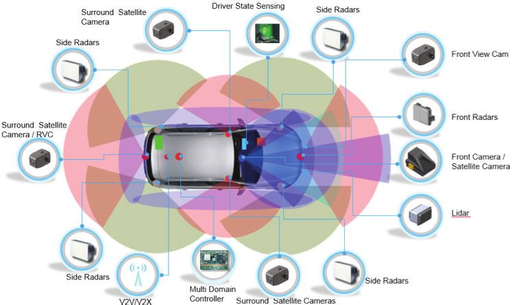
IPSR-I 2020 overview                                                                                                                                                       7

The functional performance requirements of the PIC-users are                                                              MIX
                                                                                                                    (number of designs)
important factors in determining the roadmap for future devel-
opment of PIC-technology. The IPSR-I 2019 describes the main                                                                 High

functional performance requirements of the various applica-                                           Biosensing

tions and translates these into the technological needs and
challenges to satisfy these requirements. The IPSR-I describes                                               Satcom
                                                                                                                                                         VOLUME
applications that will drive the development of PIC technology.                                                                                          PER DESIGN
                                                                                                                  Mechanical
They can be divided into high and low mix applications. Both of                               Low
                                                                                                                  Sensing
                                                                                                                                                         High
these types of driver applications can result in high production
                                                                                                                                    Lidar
volumes ; high-mix applications are typically made in many
small batches of many different products while the low-mix
                                                                                                                                              5G
applications are generated in large volumes of the same design.
                                                                                                                                            Datacom
The low-mix applications (datacenters, 5G and LiDAR) typically
have clear industrial roadmaps which are laid out by large                                                                   Low

companies. Currently, the main driver for integrated photonic                           Figure 2    Schematic sketch of applications in the volume VS mix landscape
devices are the datacenter transceivers in which the improve-
ment of the performance (400 Gb/s in 2021, 1 Tb/s in 2025)                              defined. A market that is expected to be a next major driver
is critical to the users. The low mix applications comprise                             is the market of devices enabling the (Industrial) Internet of
satellite communication, (medical) biosensing and mechanical                            Things ((I)IoT) paradigm. The market of IoT devices will com-
sensing. The graph above gives a rough overview of applications                         prise a large variety of sensors integrated with low loss wireless
based on their expected mix and volume.                                                 connectivity solutions for operations without external power
                                                                                        supply. This market is typically characterized by low prices and
For as yet, there is no consensus amongst experts on which                              high volumes.
driver type of applications will be most dominant business
driver since the high mix – low volume applications typically                           One of the main characteristics explaining the large diversity of
generate a high added value while the low mix – high volume                             integrated photonic technologies is the wavelength of the light
applications typically generate large revenues. But currently                           at which applications operate best. Below you find an overview
datacom is the main driver for technological developments,                              of the applications and their wavelengths.
because the roadmap of the functional specs are clearest

                                                                                                            N-O   N-O

      Application         ISO 20437 definitions:                                                    O-H       O-H              Molecular finger prints
         area             UV: Ultra-Violet                    Water transparancy                      C-H          S=
                          VIS: Visible
                          NIR: Near Infrared                         BIO photonics
                          IR: Infrared                                               Tele/datacom

                                    0       λ[nm]        400                            714               3000                      50.000               200.000
     Wave length
                                              UV                         VIS                    NIR                     IR                     Far IR

Figure 3   Wavelength of operation for applications1)

1)   Partial information from: Munoz P. Photonic integration in the palm of your hand: Generic technology and multi-project wafers, technical roadblocks, challenges and
     evolution; Proceedings of the 2017 Optical Fiber Communications Conference and Exhibition (OFC); Los Angeles, CA, USA. 19–23 March 2017; pp. 1–3
8

Datacenters (driving application: transceivers)

Introduction: The explosion of data generated by the growth in                                                    expected to take a higher share of the market, because of the
social networks and digital entertainment, cloud-computing,                                                       drive towards smaller photonic component solutions, lower
and IoT are the root cause of the growth of data center capacity                                                  power consumption, higher data rates, and economics in terms
and the need for high bandwidth, low-latency, low power fiber                                                     of decreasing cost per Gbps.
optics based communications. This has changed the dynam-
ics of the market of communication equipment to the point                                                         The datacom industry today are gearing up for 400Gbps sys-
that telecommunication companies are no longer driving next                                                       tems using 30-40GHz photonic devices. Customers are expect-
generation technology platforms and metrics, but the datacom                                                      ing data rates to continue to move quickly beyond 400 Gbps,
market (the datacenter industry (Web 2.0), fired by social media                                                  800 Gbps and even 1600 Gbps. Some companies even mention
companies such as Google, Facebook, Microsoft, Amazon etc.).                                                      the need for 3200 Gbps today. The obvious yet most difficult
These forces are transforming the data center architectures                                                       next move is to revisit increasing the optoelectronic device
towards a higher level of integration of photonics components.                                                    speed, and those speeds in particular that are driven not from
                                                                                                                  30-40 GHz optical bandwidth, but 80-100+ GHz (typically 40
Current status: Today, fiber-optic networks are established by                                                    GHz corresponds to 50 Gbps NRZ and 80 GHz corresponds to
a combination of long, medium and short haul optical inter-                                                       100 Gbps NRZ). Today’s roadmaps are expressing the desire,
connects that range from 3 meters to over 1000 km. PICs are                                                       but at the same time doubts about getting beyond 50 GHz.

                                             2019                          2020                             2022                                 2024                              2026                            2028

                                             400Gbps                                  800Gbps            Purple Brick Wall      1600Gbps                                                          3200Gbps
           Modules/TxRx
         Data rate density                   25 Tbps/1U                                              100Tbps/1U            Purple Brick Wall      400Tbps/1U                       1600Tbps/1U
               Form factor                  Q/OSFP                         OSFP/OBO/CP                  OBO/CP               Purple Brick Wall   Co-Pkg/CoB             Micro-Co-Pkg/CoB

                Typical link
IPSR-I 2020 overview                                                                                                           9

Main challenge: The data bandwidth demand is resulting in
                                                                   Needs < 5 years
systems with ever higher interconnect speeds, even as processor
                                                                   •   Device speed increased (bandwidths EO
speed is staying constant. Data centers need to reduce their
                                                                       S21 of 80GHz in PIC platform)
power consumption and resulting heat generation and opera-         •   Drive voltage at 1V so that drivers can be eliminated
tion costs while also managing the total cost of ownership of      •   Telcordia qualification for modulators
these systems while increasing reliability. Adding to this, data   •   Hybrid integration with InP lasers
centers have an increasing number of systems residing in an
environment of higher temperature and humidity which is also
                                                                   Needs 5-10 years
subject to corrosive elements. The resulting technological chal-   •   Device speed increased (bandwidths EO S21 to
lenge is that the technologies need to be able to support faster       120GHz+ in PIC platform (for 150Gbps NRZ data rate))
                                                                   •   Drive voltage less than 1V so that drivers can be
photonic devices of 80GHz that can operate 100Gbps NRZ or
                                                                       eliminated (direct drive from CMOS ICs)
200Gbaud PAM-4.
                                                                   Needs > 10 years
Needs: Photonic packaging technology must improve substan-
                                                                   •   Device speed increased (bandwidths EO S21 to
tially to achieve the new performance requirements for exam-
                                                                       150GHz+ in PIC platform (for 180Gbps NRZ data rate)
ple by co-packaging and on-board optics. Data centers need         •   Drive voltage less than 1V so that drivers can be
faster optical devices (such as 80GHz components), higher              eliminated (direct drive from CMOS ICs)
integration levels, higher reliability, lower power consumption,   •   Telcordia qualification for polymer modulators

a higher degree of scalable economics that address $/Gbps
metrics, and smaller more miniaturized foot-print platforms.
This is enabled by a higher level of integration, e.g. by hybrid
integration of components made out of different technologies.
10
(Industrial) Internet of Things (Driving applications: (Bio)sensing & wireless communications)
Introduction: ‘IoT’ is a system consisting of a network of This revolution will lead to a paradigm shift in technology
sensors, actuators and ‘smart objects’ connecting “all” things, requirements, having many devices leads to larger amounts of
including every day and industrial objects in such a way as to decentralized data and improved quality of data security devices.
make them intelligent, programmable, and more capable of IoT products themselves will be developed from existing applica-
interacting with humans and each other. IoT devices are being tions in sensing and communication.
developed for the consumer market (wearables), transport
(autonomous vehicles, logistics, smart homes, buildings and Even though other technologies (wireless communication,
cities, (mobile) healthcare, and the manufacturing industry. MEMs and other sensor materials) are already part of the IoT
They will revolutionize how we use the internet and drive rapid landscape, photonic components and photonic integrated cir-
economic growth. Smart Sensors with on-board or remote cuits have a substantial role to play in expanding the required
signal processing combined with artificial intelligence (AI) to network capacity and in developing high-performance, minia-
trigger automated actions enable the next industrial revolution. turized, smart photonic sensors.
UPS, batteries, RFID and NFC HVAC, Security Pumps, valves, Servers and Resource Cars, Jeeps,
generators, fuel cells, supply chain fire and monitoring, pipelines motors, storage, allocation, threat ambulances, tanks,
ambient energy control, safety purchases, robotics, PCs and analysis, troop fighter jets, radios,
harvesting, telemetry, inventory security, production, fabrication, tablets, monitoring, tactical devices,
power stations, tracking acces transportation, assembly, smartphones, intrusion storages incompatibility
smart grid, storage, sales packaging, switches and detection detection
quality control and after-sales, vessels, tanks routers
climate control PBXs
Recource Homeland security,
Buildings Surveillance border security, fire-fighting,
automation
Supply and search and rescue, medical
Meters, drills demand crisis, disaster relief,
Logistics Processes Public Equipment
enterprise tracking battlefield communications,
Mining, oil mission critical voice,
Solar panels, turbines and gas energy harvesting
and windmills Emergency
services
Alternative Smart Smart Smart Defense
Digital camera’s, energy energy industry networks & public Public Environmental
TVs, MP3s, safety infrastructure monitoring, law enforcement
gaming consoles Entertainment and public protection
Power systems, Safety Smart The internet Smart POS terminals, cash
Stores
sockets, alarms living of things retail registers, tags, vending
Awareness machines, cameras, signs,
Thermostats, customer experience and
refrigerator, ovens, Efficiency focused market
Smart Smart Smart Smart Assisted driving
e-readers and health city farming transport
desktops, Care Robot taxi
washers/dryers, Mobile ticketing
lights
In vivo / home
research Leisure Traffic Agriculture Transport Item location, anti-theft,
Wearables, wellness control NFC payment
monitors, trackers systems
Connected City (non-vehicular
information Environment
community and vehicular)
model
MRIs, PDAs Vehicles, lights, ships,
telemedicine, planes, signage,
medical devices, Social Smart gyms, CCTV, ITS, Weather Soil analytics, tolls, condition based
implants, networking, socials sports, structural traffic flow, prediction, fleet, storage (water and maintenance,
surgical equipment, historical smart health, congestion species fuel tanks) and waste usage based design,
chronic diseases queries, museums, noise maps, avoidance, tracking management, livestock pre-sales analytics,
losses enhanced waste smart parking monitoring, fish farming, real-time routing and
and thefts game rooms management forestry tracking
Industries and sectors Application groups Devices
Figure 5 Proliferation of devices and applications in the Internet of Things (IoT)3)
3) Fraga-Lamas, Paula. (2017). Enabling Technologies and Cyber-Physical Systems
for Mission-Critical Scenarios. 10.13140/RG.2.2.22769.79202.IPSR-I 2020 overview 11
Current Status: The number of devices currently connected to (Data security)
the internet per person is 4~5. Rapid growth in the consumer Security of the data and network has been recognized as critical
market takes advantage of existing networks to connect weara- for successful adoption of this technology, for example where
ble devices (e.g. smart watches for health care monitoring) and critical infrastructure is controlled. Blockchain and soft-cryp-
home or office wireless networks for environmental monitoring tography will secure data for the time-being, with quantum
and control, and security and access monitoring. Internet photonics being a potential longer term solution.
Protocol version 6 (IPv6) together with 5G and narrower band
networks are being developed to deal with the anticipated Needs: If the amount of installed fiber will explode mainly to
growth in the number of addressable IoT devices and data traf- support shorter access links within cities, the required inte-
fic, and the required end-to-end quality of service (particularly grated photonic devices having a smaller size and lower cost will
for mission critical applications in health care, autonomous need to be developed. Sensors which are self-powered (energy
vehicles and security). harvesting) where appropriate will need to become cheaper,
faster and better performance to help drive demand. Sensing
Sensors are already in development or marketed for integration functions will also need to be integrated with wireless con-
in consumer goods (infotainment, wearables, food and water nectivity functionality and some level of signal processing so
quality), eHealth (blood, breath and other chem-bio sensor standardized information, not raw data, is transmitted through
analysis), energy and building automation, industrial (man- networks.
ufacturing) automation and structural monitoring, environ-
mental monitoring (oil and gas distribution, drugs, hazardous Sensors will need to become solid-state, miniaturized, and dras-
materials and climate change). In transportation, visible and IR tically lower cost for significant consumer market penetration
imagers for highway monitoring along with LIDAR and other and eventual full autonomy.
sensors are already being developed for autonomous vehicles.
< 5 year Needs
Main Challenges: (Network capacity and reliability) IoT is
• Secure data transmission protocols
anticipated to grow rapidly to the point where cities will have • Increased network capacity for IoT data
one smart “thing” per square meter. New wireless cellular net- • Higher wireless bandwidth, low latency
works will need to deal with this device density and volume of • Sensors with sufficient sensitivity, accuracy and specificity
data generated by it. End to End Quality of Service must address
5-10 year Needs
high reliability, low latency and a sufficiently high data rate to
securely handle bidirectional data for each application. Mission • Localised signal processing
• Low-C SWaP
critical applications require round trip data exchange of~ 1
• Miniaturized systems (packaging)
millisecond or less. Managing minimal service interruptions for • Portability, power autonomy for mobile applications
mobile users (e.g. in automobiles and trains) is an additional
networking requirement. Needs > 10 years
• Real-time data analysis and use of AI
(Low costs, size, Weight and Power Consumption) • Localised decision making
The actual IoT devices contain some kind of sensor and a (5G
wireless) datacom unit. The photonic components and PICs
required for these expanded 5G networks and IoT sensors will
need to take into account demands on Cost, Size, Weight and
Power consumption.12
Automotive (Driving applications: LiDAR & wireless communications)
The opportunities for Integrated photonic modules can be The harsh environment and the high temperature requirements
found in Advanced Driver Assistance Systems (ADAS) which force development improvements in components and materi-
helps the driver to safely navigate their journey. Eventually als. Components must operate at a high temperature without
these ADAS systems might not require a driver anymore, substantial de-rating or functional performance decrease, and
making the cars fully autonomous. The two main opportunities without additional cost. Materials such as laminates, solder
for PICs within the ADAS systems is improving the quality of masks, adhesives, under fills, coatings, and solder need to
LiDAR for an acceptable cost point, and fully integrate the car’s perform at high temperature extremes and environmental
systems in intra- and inter-car communication networks. There conditions (i.e., moisture and chemical exposure) without
are also opportunities for environmental sensors like air and degradation.
oil quality, but these will not be discussed in the automotive
chapter but in the sensing chapter. Most experts anticipate that Advanced Driver Assistance
Systems will require numerous sensors and low cost LiDAR
Increasing density is important for these applications because (Light Detection and Ranging). The cost target for LiDAR
of cost, size, and weight reductions. Because of the high reliabil- systems is expected to fall between $250.- and $500.- because
ity requirements it is important to have assembly and manufac- there are competitive sensors and proprietary algorithms to
turing equipment available with high requirements. Automotive integrate the visual, RF, and IR information which replace the
applications are extremely cost sensitive. The challenges for need for LiDAR.
the use of PICs in the automotive industry is to adapt to other
markets’ technologies to meet the high temperature, environ-
mental, and reliability requirements cost effectively.
Figure 6 Subset of sensors used for autonomous vehiclesIPSR-I 2020 overview 13
Aerospace (Driving applications: Wireless communications, Mechanical sensing, Biosensing, LiDAR)
Introduction: In the aerospace market it is increasingly rec- Needs: In the near term the aerospace market seeks improve-
ognized that PICs are an enabling technology giving improved ments in the core technology readiness level of existing PIC
performance over existing electronic and photonics solutions capabilities, focusing on improving the reliability to deliver
as well as enabling new market applications such as embed- predictable photonics performance throughout the supply chain
ded structural health monitoring. Aerospace applications are and the lifetime of the product. Longer term developments are
continually seeking stringent improvements in size, weight, and typically looking for more efficient power usage, which may be
power along with improved reliability. Unlike other markets attained by either better hybrid combinations of PIC plat-
such as data-centers and automotive, aerospace applications forms or increased monolithic integration of electronics and
are capable of paying a premium to attain these improvements, photonics.
making the aerospace market an ideal market for early adoption
of PIC-based appliances. Aerospace covers a broad spectrum of Needs < 5 years
photonics applications but in particular Datacom and Sensing
• Reduced Foundry process variance
applications, • Qualified packaging for harsh environemnts
• Qualified PIC electronics, e.g. drivers and TIAs
Current status: PICs are being actively adopted for numerous
aeronautics and space Sensing and Wireless communication
applications. There is also increasing industrial aerospace
research and development as demonstrated by the growth in
the number of aerospace PIC patent applications.
Both ESA and NASA continue to be actively investing in the
developments of core PIC technology development with numer-
ous programs. ESA’s photonics roadmap outlines its expectation
for the main satellite primes (Airbus, OHB, Thales Alenia
Space) to be offering satellite operators PIC based photonics
solutions by 2020 and that PICs will be the adopted “standard”
over the decade 2020-2030.
Main challenge: For increased growth in the adoption of PICs
in Aerospace the main challenges are typically related to the
high reliability qualification standards. Aerospace product
performance metrics typically have stringent tolerances in
which mature supply chains without large variation in expected
performance or process capability are indispensable for the
product development cycle and adoption of PICs. These issues
are valid for both foundry process capability and the quality of
packaging and assembly.14
Biosensors & medical (Driving applications: Biosensing)
Introduction: The IPSR-I Biophotonics Product Emulator Challenges: The main challenge for these applications is getting
addresses integrated electronic-photonic technology applica- the cost per chip down, which can be mainly achieved by
tions for sensors and other products needed by the healthcare rapid and easy prototyping since volumes per chip design are
industry for health diagnostics and monitoring, as well as relatively small. It should be noted that there is a tipping point
control of air, water and food safety and quality. Together these in cost target where volumes can get very high for disposable
applications often are addressed as Biophotonics. applications. Another challenge is the interfacing (coupling of
the light) of the object to be measured with the PIC.
Current status: There are a number of sensor applications that
could be met with integrated photonic technology, but there are
also competing technologies, such as MEMs, that could meet
some current application needs. This chapter addresses biopho-
tonic’s needs and identify markets that might be early adopters
of integrated photonic systems technology; the sensors chapter
discusses the technological needs.
Life Science & Health
In-Vivo In-Vitro
Life science labs Biomedical analysis
Hospitals and clinics laboratories
Veterinaries Life science labs
Physicians Hospitals and clinics
Specialists Quality auditor
Patients Patients
Veterinaries
Imaging Diagnostic and Microscopy
analysis imaging Optical microscopy
systems
Surface imaging,
inside imaging,
see-through imaging
Analytics, Sensing Diagnostic sensing Analytical systems
systems Sequencing,
Oximetry cytometry,
measurement spectometry,
biosensors
Processing, Curing Laser processing & curing
Proces treatment, laser surgery
Figure 7 Biophotonics market segmentation in Life Science and Healthcare4)
The early opportunities for PICs that have been identified are
tissue imaging (specifically Optical Coherence Tomography
(OCT)), (trace) gas- and liquid sensing, wearable sensing
(including spectrometry) and point of care diagnostics
(including disposables).
4) Courtesey of TematysIPSR-I 2020 overview 15
16

     Front-end
     technology

        Chapter 2
IPSR-I 2020 overview 17
Introduction: Unlike electronic integration where silicon is
the dominant material, PIC-technology uses a large variety
of material platforms, including electro-optic crystals such as
Silicon, Silicon Nitride, Indium Phosphide, Gallium Arsenide
and polymers. The different material platforms are used because
they each provide different advantages and limitations depend-
ing on the function to be realized. The limitations of optical
properties of the various platforms can be gradual in the sense
of differences in price/performance ratios between the tech-
nologies, but also quite discrete, e.g. able to generate light or
not. This necessitates a careful consideration of the technology
platform or platforms to be used, depending on the specific
application in mind.
Platforms InP SiN SiPh GaAs Polymers
Operating optical window (nm) 1300 - 2000 400 - 2350 1300 - 2000 700 - 1000 400 - 1000
Wafer size 3" - 4" - 5" - (6") 4" - 6" - (8") 4" - 6" - 8" - (12") 3" - 4" - (6") Spinning on any
substrate
Index & (contrast %) 3,4 (10%) 1,8 (25%) 2,5 (>100%) 3,2 (10%) 1,8 ( 50 μm > 10 μm 100 μm > 500 μm
Attenuation (dB/cm) 2,5 < 0,1 3-4 5 < 0,1
Birefringence < 1 x 10 4
< 1 x 10 4
< 1 x 10 3
< 1 x 10 4
n.a.
Footprint (typical PIC size 200 x 300 μm 2.000 x 4.000 μm 200 x 300 μm – 3.000 x 4.000 μm
CMOS compatibility No Yes Yes No Yes
Fiber chip coupling accurate Very good edge accurate – Easy
alignment via coupling alignment via
edge coupling grating coupling
PIC cost Moderate Good Moderate – Low
Packaging cost Challenge Good Challenge Low
Applications Datacom, Datacom, Datacom, Datacom, Optical
interconnects, interconnects, interconnects, interconnects, interconnects
tunable lasers, visible light sensors, high power lasers
optical switches, sensors, receivers,
transceivers, antenna's, OCT, WDM devices
optical amplifiers, lab-on-chip, hybrid
WDM devices, lasers with InP,
receivers 5G, RF analogue
links
Figure 8 Overview of the properties of PIC platforms
Another important consideration to use a material platform
is the potential co-integration with other technologies like
micro-fluidics or micro-electronics and the availability of
(mass) manufacturing capability. E.g. the Silicon Photonics
(SiPh) platform is strongly promoted due to its monolithic
integration capability with CMOS-electronics and the wide
availability of silicon processing capabilities, opposed to the fact
that the application of SiPh might be less advantageous from a
basic technological point of view, in particular since it has no
intrinsic light generating capabilities and can handle a limited
wavelength range.18
0 λ[nm] 400 714 3000 50.000 200.000
Wave length
UV VIS NIR IR Far IR
III-V semiconductors ISO 20437 definitions:
SINx/SIO2 UV: Ultra-Violet
VIS: Visible
Substrate SI/SIO2 (SOI) NIR: Near Infrared
material Ge/SI IR: Infrared
Silic
Silicon
Germanium
Heavy-metal oxides
Chalcogenides
Figure 9 Wavelength of operation of PIC platforms and materials5)
One of the main challenges that is addressed in almost all
application areas is the critical cost point per chip. For the Cost Breakeven point
high-mix – low volume applications the main cost driver is the per
chip
cost for prototyping and development, for the low-mix – high
volume applications the production cost leaves a large footprint
on the cost. To reduce costs, larger volumes are needed which
Market volume
will allow development of fully automated processes resulting versus cost/chip
in an adequate economy of scale. As described in the appli-
cations section, datacom will be one of the first applications
Cost/chip versus
driving down the cost per chip. It is expected that more applica- production volume
tions are needed to drive the cost down further.
In the IPSR-I, the four main PIC material platforms are dis- Range of profitability Production volume
Market volume
cussed: Silicon Photonics, dielectric materials (such as Silicon
Nitride), InP as the main representative of III-V semiconduc- Transition
barrier
tors, and Polymers.
Figure 10 . a) A standardized technology requires substantial production volume for
reaching a maturity and a strong market volume to become profitable6)
Cost
per
chip
Cost per chip ~ 1/volume
Growing sets
of markets
Market volume
versus cost/chip
Production volume
5) Partially inspired by: Munoz P. Photonic integration in the palm of your hand: Market volume
Generic technology and multi-project wafers, technical roadblocks, challenges
and evolution; Proceedings of the 2017 Optical Fiber Communications
Conference and Exhibition (OFC); Los Angeles, CA, USA. 19–23 March 2017;
Figure 10 b) Growing set of markets ramp up the production volumes
pp. 1–3
to provide low cost6)
6) Courtesey of Roel Baets, IMECIPSR-I 2020 overview 19
Silicon photonics
Introduction: The semiconductor material silicon is transpar- Integrated photonics technology has entered into the healthcare
ent to infrared light of wavelengths above about 1.1 microm- space with medical devices and diagnostic sensors. It may pro-
eters. For this type of light, silicon has a very high refractive vide solutions for various health diagnostics: spectrometers for
index, of about 3.5. The tight optical confinement provided diagnostics by measuring specific substances in tissue, skin or a
by this high index allows for microscopic optical waveguides, blood or urine sample, biomedical imaging for cancer research
which may have cross-sectional dimensions of only a few using photoacoustic sensors, optical coherence tomography,
hundred nanometers. Single mode propagation can be achieved, cytometry and detectors for cardio vascular disease detection.
thus (like a single-mode optical fiber) eliminating the problem
of modal dispersion. Monolithically integrated advanced active The ability to provide large-scale integration of photonic func-
optical functions of modulation and detection of optical signal tions on chip by silicon photonics opens up the opportunity
at very high speed, integration with electronics, and reliable to use this technology in other sectors such as building and
topologies for integrating laser devices with silicon PICs at construction sector, energy sector and manufacturing sector
wafer scale have consolidated the field of silicon photonics. where silicon photonics sensors can be used for structural
health monitoring, bearing condition monitoring and turbine
The technology platform is highly enabled by low-cost mass efficiency. In the automotive and transportation sector silicon
manufacturing of silicon PICs using the widely enabled CMOS photonics can provide LiDAR solutions and beamformers with
processes and toolsets. Its products are hitting a diverse set of wide steering angles.
market sectors such as optical communication, Lidar, sensing
and medical. Needs:
The next years are bound to see further strengthening of silicon < 5 year Needs
photonics technology by improved performance of passive
• Optical power supply solution
building blocks, active building blocks and gain blocks with • High radix matrix switch solution: >64 x 64
enhanced reliability and robustness. The Process Design Kits are • Distributed gain block solution
already on their way to be more complete by the inclusion of • I/O and power distribution for 2.5D photronics
• SM-everywhere compatibility
compact models enabling the creation of very large scale silicon
• Athermalization and/or scalable tuning:
PICs. Furthermore, unified approaches to integrate photonic filters modulators, lasers
processes into electronic processes without compromising the • Wafer level inspection (High throughput
process stability are likely to consolidate. photonic test, known good die, CAPEX)
5-10 year Needs
Current situation: Currently the biggest driver for silicon
photonics technology is high-speed optical communication • Pervasive gain blocks with standard devices
• I/O and power distribution for 3D photronics
in the complete range from very short range (on-board or
• Wafer level inspection (functional test & Build In Self test)
even on-chip) to medium (metro-networks, intra-datacenter
communication) and long haul telecom and datacom. Photonic
interconnection is currently being accomplished with a range
of (hybrid) multichip solutions, including SiPh, GaAs and
InP devices in various transceiver modules and active cable
assemblies.
Universal industry goals are i) to achieve acceptably low power
budgets; ii) to provide photonic signaling in the Tb/s range, and
iii) to use lower cost Si/CMOS production capabilities, where
possible including existing processes, to reduce the cost of
photonic systems.20
Silicon Nitride
Introduction: Silicon Nitride waveguides have a number of With regards to switching and modulation, very reliable but
advantages over alternative technologies. Low propagation loss, rather slow modulation are available with-known thermal
wide range of transparency, low cost, good reliability for high phase modulation in case of SiN (limited to 1 kHz). Faster
power and industrial operating conditions, as well as good modulation up to the MHz and the GHz regimes are available
coupling to single mode standard fiber. The propagation loss using PZT material [2]. In case of (quasi-) DC operation, these
of 0.5dB/m allows to achieve filters with high finesse which modulators furthermore reduce the required switching power to
are required in for example narrow line width external cavity a few microWatts only.
laser but also for example to improve sensitivity of resonant
micro optic gyroscopes. In sensor applications Nitride has Multi Project Wafer (MPW) runs operating @1550 nm and VIS
benefits in low loss over a wide range of wavelength from visible are available since 2011. In these MPW services, fundamental
to the mid-infrared. For high speed datacentre transceivers building blocks are available, including the optical waveguide,
of 400Gb/s and beyond, loss has become even more critical thermo-optic phase tuning elements, Y-branches, MRR’s, direc-
as multi-bit amplitude modulation reduces the power level tional- and Multi-Mode Interference couplers.
between the bits. So, in order to achieve the same signal to
noise ratio, the power levels in the fiber and from the chip need Needs:
to increase proportionally. Currently, the hypercloud data-
centers experience a massive delay in the delivery of 400Gb/s < 5 year Needs
transceivers due to the additional power requirements which
• Extension of the guiding range from 0.4-5 µm
existing suppliers cannot meet reliably. Low loss Nitride tech- • Increase level of integration of light sources, modulators
nology meets the conflicting demands on small footprint and and detectors need to be heterogeneously and
low loss that currently can’t be solved by other platforms. monolithically integrated onto the SiN platform.
• Development of transfer printing processes for the
hybrid integration of sources and detectors, at the
SiN can meet the requirements for some applications where different wavelength ranges in 0.4-5 µm [20]
it is also important to handle high power densities. This is for • Investigation of maximum optical power that
example the case in future 5G networks where optical mux and can be handled by SiN waveguides.
• Smart integration of SiN platforms with
demux devices will be installed to connect antennas to the base
microfluidics for life science applications
station. For these applications the antennas may be at a short
distance from the base station resulting in multiplexed powers
of the order of Watts. Optical chips in 5G antenna’s should
7) Blumenthal, D.J., Heideman, R., Geuzebroek,D., Leinse, R., and Roeloffzen,
have coupling efficiency to standard single mode fiber which C., Silicon Nitride in Silicon Photonic. Proceedings of the IEEE, Vol. 106, No.
12, December 2018.
are better than 90%. SiN can achieve 99% coupling efficiency, 8) Briefing on PZT based stress optical tuning on TriPleX platform.
also for heterogeneous and hybrid integrated solutions. A recent
comprehensive review of the latest progress on SiN technology
platform and integration with active components can be found
in reference [1].
Current status: Silicon Nitride fabrication processes are
already mature. SiN layers with uniform thicknesses and repro-
ducible refractive indices are deposited using both LPCVD and
PECVD. For Silicon nitride waveguides both stepper lithography
as well as contact lithography can be used, considering the
relatively low effective index compared to Si, allowing relatively
large waveguide widths while maintaining single mode charac-
teristics. Using typical commercially available stepper lithogra-
phy tools, lines/spaces of 250 nm can be fabricated.IPSR-I 2020 overview 21
III-V semiconductors, in particular InP
Introduction: A key feature of III-V compounds is that they Needs:
exhibit a direct bandgap enabling efficient generation and
amplification of light, as opposed to indirect bandgap semi- Needs < 5 years
conductors like silicon and germanium. This has resulted in
• Fully automated process equipment (epitaxy/
the development of a wide range of semiconductor laser types deposition, etching) with cassette loading
(CW, tunable, multi-wavelength, pulse, frequency-comb, single • Improved reproducibility of epitaxy/
photon) for use as transmitters. Materials based on GaAs (gen- deposition and etching ( 10 years
Challenges: The main challenge for InP is the lack of a large-
• Move to InP processing on silicon substrates (8” and larger)
scale manufacturing infrastructure. Although the existing
infrastructure is adequate for today’s market, the expected
increase in growth will require major investments in scaling the
infrastructure for manufacturing and testing to align with the
expected market size. As highest technical priority we see adapt-
ing of today’s manufacturing equipment to fully automated
operation, since most of them are still operated manually.. For
increased operational efficiency and performance it is impor-
tant to move to larger wafer sizes. In the longer term to adopt
to 200 mm wafers, the transfer from InP-substrates to silicon
carrier substrates is envisaged, while keeping the photonic layer
in InP and its compounds.
The future needs with respect to the basic technology to allow
for improved performance highly depends on the photonic
building block under consideration. Also the improved man-
ufacturing capability in terms of precision and resolution
will ultimately enlarge the component design space and
advance building block performance. Another priority is in
PDK-development and automated testing. PDK development
and automated testing for InP has a large synergy with silicon
photonics.22
Polymers
Introduction: Polymer (organic) compounds based technol- Needs:
ogies for photonic applications have been developed by both
academia and industry over the past 40+ years. Both active and Needs < 5 years
passive polymers have been researched, optimized, developed
• Device speed increased (bandwidths EO S21 of
and made into products. 80GHz (polymer modulator) in PIC platform
• Drive voltage at 1V (polymer modulator)
Current situation: Unlike conventional modulator materials so that drivers can be eliminated
• Telcordia qualification for polymer modulators
such as InP, Lithium Niobate, silicon photonics and GaAs, the
• Hybrid integration with InP lasers
polymer material system is naturally fast. The polymers provide
low loss and further good optical quality to enable fast optical Needs 5-10 years
signaling on-board and board-board via optical backplanes.
• Device speed increased (bandwidths EO
Currently, commercial high speed optical modulators are made S21 to 120GHz+ (polymer modulator) in PIC
of electro-optic polymers that will be capable of 100 Gbaud platform (for 150Gbps NRZ data rate)
or 100 Gbps and beyond. Technical data showing 130 GHz • Drive voltage less than 1V (polymer modulator) so that
drivers can be eliminated (direct drive from CMOS ICs)
corresponding to 150 Gbaud) indicates that even higher speeds
• Telcordia qualification for polymer modulators
should be possible in the future. Polymers are perfectly suited
for adiabatic coupling which is the main enabler for silicon Needs > 10 years
photonics – WDM systems.
• Device speed increased (bandwidths EO
S21 to 150GHz+ (polymer modulator) in PIC
Challenges: The key application for photonic based polymers platform (for 180Gbps NRZ data rate)
has been fiber optic communications in which technology ena- • Drive voltage less than 1V (polymer modulator) so that
bling increasing data rates is under severe scrutiny. The obvious drivers can be eliminated (direct drive from CMOS ICs)
• Telcordia qualification for polymer modulators
yet most difficult next move is increase the optoelectronic
device speed, and those speeds in particular that are driven not
from 30-40 GHz optical bandwidth, but 80-100+ GHz (typi-
cally 40 GHz corresponds to 50 Gbps and 80 GHz corresponds
to 100 Gbps). At the same time, these new optoelectronic
devices must be very small, and operate with very low voltage to
keep power consumption low.IPSR-I 2020 overview 23
24

      Back-end
     technology

        Chapter 3
IPSR-I 2020 overview 25
Packaging
Introduction: Packaging of integrated photonic devices presents Packaging can be seen as the assembly of photonic and elec-
numerous technological, manufacturing and cost challenges. tronic devices from chip to board, encompassing optical fibers,
Historically, packaging has been accepted to be a high-cost micro optics and electronic IC packaging using wirebonding
step in the overall manufacturing process, often consuming and flipchip assembly. Additionally, it comprises thermal
over 80% of the total manufacturing cost. However, as poten- management and mechanical housings including hermetic
tial mass markets for integrated photonics open up and unit and non-hermetic packages. The figure below provides a broad
demand steadily increases, a clear roadmap for more cost-ef- overview of the key packaging technologies used to produce
fective and volume scalable packaging processes of integrated integrated photonic modules.
photonic devices becomes more critical..
PHOTONIC DEVICE
Optical Integration Electrical Thermal Mechanical
Interposer Free space Optical fiber Hybrid Interposer
integration Active Hermetic
cooling
Micro Passive Non-hermetic
optics Grating PCB Micro-interposer cooling
coupler Micro End
Edge optical facet
coupler
Wirebonding Wirebonding
Lensed Flipchip Flipchip
fiber
Fiber
array
2.5D 3D 2.5D 3D
Figure 11 Organization chart providing a breakdown of the key packaging technologies, including; optical, electrical, thermal and mechanical aspects.9)
Current status: Current photonic packaging processes typically A major development in future packaging will be the transi-
rely on serial or device-level packaging of individual modules. tion from device-level to wafer-level packaging. Increased use
Such processes have been in use for many years but are only will be made of new substrates and interposers to co-package
viable for high-cost and low-volume applications such as photonic and electronic devices in more compact sub-systems.
advanced fiber optic telecommunication. However, with the Wafer-level packaging provides a route to improved scaling of
rapid growth in applications such as datacenters and sensors the manufacturing process, ensuring packaging is economically
for the Internet of Things, current packaging processes are inca- viable, especially for mass market applications. As integrated
pable of meeting emerging market demands and this present a photonics become a more widely used technology platform,
critical manufacturing and cost bottleneck. the high-volume assembly and packaging processes used in
electronics manufacturing will become more common-place for
Challenges: The main challenge to be addressed at present is photonic manufacturing. Such wafer-level packaging processes
the ability to package photonic devices in large volumes and at will start to be adopted during the next 5 years, becoming more
costs that meet market demands. standardized in 5-10 years.
9) Courtesey of Peter O’Brien, Tyndall National Institute26 New precision packaging equipment and tools will be required to implement these advanced manufacturing processes. There will be a greater use of automated and passive optical align- ment processes using advanced machine vision and robotic systems, moving away from existing operator assembly pro- cesses. Operator driven assembly is not only unsuitable for very high-volume manufacturing but is also unsuited to delivering the sub-micron alignment tolerances required for complex multi-channel integrated photonic devices. Developments in this area will also benefit from advances made in packaging equipment used for advanced electronics assembly. New materials will also be required to facilitate increasing demands for improved optical, electrical and thermal perfor- mance. For example, as photonic modules become more com- pact, there will be an increased demand to effectively manage heat dissipation though passive (non-thermoelectric) solutions. This will require new materials with improved thermal conduc- tivities and which exhibit the extended lifetimes required for robust photonic modules. New materials will also be required to facilitate low-cost non-hermetic packaging of photonic devices. Although non-hermetic, these encapsulation materials must act as a barrier to moisture ingression, have excellent thermal conductivities to dissipate heat from the package and impart minimum stress, ensuing long lifetimes in harsh operating environments. There will be a growing demand to develop co-packaging designs, incorporating photonics with electronics, MEMs and microfluidics. For example, point-of-care (PoC) diagnostics will require a photonic sensing platform to be co-packaged with microfluidics for sample delivery and electronics for in-situ sig- nal analysis. PoC diagnostic devices have the potential to open mass consumer-driven markets, so wafer-level packaging will be essential to enable cost-effective devices. Finally, all of the above developments will need to align more closely with design rules and standards. A coherent set of packaging design rules and standards facilitates developments and use of new processes, materials and equipment supporting future supply chains, from design and foundry, through to packaging and test.
IPSR-I 2020 overview                                                                                                                                     27

Interconnects

Introduction: The chapter on interconnects focusses on the tech-                      edges of the signal processing boards. As the data rates at the
nologies that are used for realizing optical connections between                      data center will continue to increase, also the broadband board
integrated photonic components. In this, two main domains can                         level and intra-rack copper based interconnects will be replaced
be distinguished: the first concerns the optical communication                        by optical communication links.
at substrate level, connecting electronic/photonic components
such as electronic and photonic ICs that are combined in a                            Further expansion of the interconnect technology domain
single package or bare electronic and photonic IC’s mounted on                        results from the needs of novel applications in markets like the
a substrate and communicating across or to/from the substrate.                        sensor, medical and 5G markets, which have started to apply
The second domain is related to optical connectors that are used                      integrated photonic technologies recently.
for realizing an optical connection between e.g. two optical fibers.
                                                                                      Main Challenges: To cope with the further increasing on-board
Current status: The current optical (data) paths to/from a                            data rates and the optical interconnection needs of future
board make use of arrays of optical fibers which are connected                        photonics applications, optical (embedded) interconnections
to photonic transceiver components at the edges of the board.                         needs to be introduced at board level. These interconnections
The intra board communication and the backplane commu-                                will replace (1) discrete optical fiber based connections between
nication is being handled by electrical connections that are                          optical components on a single substrate and (2) copper inter-
embedded in the boards and via backplane connectors.                                  connects over relatively short distances. The driving forces for
                                                                                      pursuing these goals are to realize: higher bandwidth*distance
Fiber optic connector technology is well advanced, having a                           product, reduced power dissipation, reduced noise and cross-
30-plus year history of development and manufacturing for a                           talk, improved signal data rate density (Gb/sec/cm2 of board
wide range of applications and densities. The current generation                      edge area) and reduced interconnect form factor.
of connectors are relatively costly and sensitive to interruption
of signals by dust and other contaminations. A special type of                        There are five application areas classified by the length of the
fiber-optic connector is the expanded beam connector which                            optical link for which a technology approach for the next
is used to avoid the interruption of signals by dust or other con-                    generation has been defined:
taminants and reduce mating damage by eliminating glass fiber                         1. rack-to-world connections;
to fiber contact.                                                                     2. rack-to-rack connections;
                                                                                      3. inter-blade connections between blades in a single
In present day data centers most of the copper based rack-to-                                rack (potentially through an optical backplane);
rack datacom links have been replaced by broadband optical                            4. intra-blade connections between modules on a single blade;
communication links, using pluggable optical modules at the                           5. intra-module connections within a module.

  (A)   Pluggable midboard SM/MM modules, to reduce copper trace length and related impairments
  (B)   Expanded beam SM/MM connectors to reduce precision requirements and contamination sensitivity
  (C)   Low-mating-force, dust resistant, high density front panel

               (B) & (C)              FO cable (SM/MM)                        (B)                (A)

                                                                                         Midboard optic                    FPGA/ASIC

                                                                                                                                                PCB

                                                                                                            Copper trace

Figure 12 Technology approach for next generation systems in Application Areas 1 and 2.10)

10) Courtesey of Terry Smith (3M, retired) and Peter Maat (Astron)
28
(A) Pluggable midboard mount transceivers with fly-over fiber-based media
(B) Optical embedded waveguides including optical interfacing to optical front panel / backplane
(C) Optical backplanes simplifying PCB to PCB optical routing
(D) Expanded beam front panel, backplane, and midplane optical connectors
(B) (D) (A)
Midboard optic FPGA/ASIC
PCB
(C) Copper trace
(D) FO cable (SM/MM) (A)
Midboard optic FPGA/ASIC
PCB
Copper trace
Figure 13 Technology approach for next generation systems
in Application Area 3.11)
(A) Reflowable electronic/photonic integrated modules to eliminate manual placement of modules
in copper sockets (but still requiring manual coupling of optical conectors)
(B) Interposer on PCB to provide electrical and optical traces connecting separate modules
on the same interposer, to isolate modules from PCB reflow process
(C) Optical embedded waveguides incluiding optical interfacing to optical front panel/backplane
Copper trace
(C) (A)
EOIC EOIC
OEIC
(B)
Optical waveguide
Figure 14 Technology approach for next generation systems
in Application Area 4.12)
11) Courtesey of Terry Smith (3M, retired) and Peter Maat (Astron)
12) Courtesey of Terry Smith (3M, retired) and Peter Maat (Astron)IPSR-I 2020 overview 29
Additional interconnect advancements in the development
Needs < 5 years
of improved expanded-beam SM connectors are needed to
facilitate high volume deployment of optical interconnects by • > 16 fiber SM expanded beam connectors, for cables
and modules with manual termination
overcoming dust contamination, damaged fiber interfaces and
• SM expanded beam connectors, for optical backplane
reducing thus preventing costly cable cleaning and inspection connectors, frontplane, and midplane applications.
procedures in the field. • 24 port module optical interface using pigtail,
1D waveguide array pitch converter
• Module-board attachment via socket
To enable wide-scale deployment of substrate-level optical inter-
connects, the following technology gaps and related infrastruc- Needs 5-10 years
ture gaps must be addressed:
• > 32 fiber SM expanded beam connectors, for cables
and modules with semi-robotic termination
•• low-mating-force environmentally-robust, contamination- • Low loss optical waveguides for
resistant low-optical-loss connectors for SM systems, e.g. integration in PCBs ( 64 fiber SM expanded beam connectors,
•• solder reflow compatible packages and connectors for
for cables and modules with robotic termination
integrated optics modules, • >128 port module optical interface using multicore
fiber, 2D waveguide/microlens array, interposer
•• optical coupling component “tool kit” or process design kit
providing low-loss coupling components suited to a wide
variety of PIC designs and foundries, for chip edge, surface
grating and adiabatic evanescent coupling to PICs,
•• Low loss substrate-embedded SM waveguides, compatible
with solder reflow, that can eliminate the need to manually
installed fly-over fiber optic cables on board-mount modules30
Assembly
Introduction: Assembly is the process of bringing together Main Challenge: The main challenge in assembly of optical
components, aligning them accurately with respect to one devices is cost reduction to make them economically viable
another and then joining them permanently utilizing a variety in more applications. An important issue in reducing cost is
of processes. As compared to typical microelectronic com- the relatively small volume (tens of thousands) of photonic
ponents, photonic devices have additional, unique assembly devices that are build, as compared to millions of electronic
requirements such as fiber attachments, sub-micron alignment devices. This makes the development of new assembly processes
accuracy, Z axis assembly, particle elimination, etc.. unattractive since the potential revenue from the sale of these
processes is often not large enough to recover their develop-
Since packaging and assembly is a large fraction of the cost of ment costs.
current devices, the focus of this chapter is on reducing these
costs. A current important challenge is reducing the cost of sub-
micron fiber and fiber array alignment. Another challenge is
Current Status: Many applications require single mode optical developing methods to eliminate optical fiber pigtails. Their
interconnects where alignment, especially of fiber attachments, inclusion makes manufacturing difficult and expensive.
are subject to submicron tolerances and stability over the Alternatives such as waveguides built into substrates and circuit
lifetime of the product.. Generally, rigid materials with high boards are emerging as an alternative solution. This will require
modulus of elasticity and low thermal coefficient of expan- new assembly processes between components and waveguides
sion are best and are used extensively in optical assemblies. on substrates and in boards.
Unfortunately, these materials tend to be expensive, therefore,
much research effort is spent on switching to lower cost materi- Developing a robust supply chain for parts with needed charac-
als and lower cost processes to apply these materials. teristics such as fiducials, tight tolerances, smooth, straight flat
edges, good plainarity, consistent lot to lot properties, etc. for
Another obvious way to avoid assembly cost is to minimize optical products is a challenge.
the number of components to be assembled. That is being
addressed by integration at the platform level in the front-end. Increasing volumes of the high mix nature of photonic manu-
Unfortunately, not all of the functions needed in optical appli- facturing calls for a new generation of assembly processes that
cations can be integrated monolithically, so separate compo- is enabled by new equipment which is tooled and programmed
nents made with different platform technologies are combined with high flexibility and with high (submicron) precision for a
by what is now called heterogeneous or hybrid integration. new product and easy to reset for repeated jobs..
Assembly needs are dictated by the trend to make optical Another need is for the detailed mechanical and optical prop-
devices smaller. As mentioned, the inclusion of single mode erties of the materials used in optical products that are often
components requires sub-micron bond line thickness control not available. Standardizing on those materials and making the
in joints and location tolerances. In addition, sensors not properties available will enable designers to model optical prod-
only comprise PICs but also other specialized components ucts better and minimize the need to build and test hardware.
that impose constraints on the assembly process, restricting
assembly options. Many optical devices incorporate compo- Finally standards are needed to minimize development efforts
nents which are sensitive to environmental conditions, e.g. InP, and enable solutions, once developed, to be used in many
SiN, GaAs and GaN substrates, polymer based devices. Finally, devices. As with other industries, standards will emerge as vol-
optical devices are often 3 dimensional rather than planar. The ume grows, new devices are introduced and incorporate parts
net result of these unique more demanding requirements is and processes that are available.
that new joining methods utilizing new materials and process
equipment are needed.You can also read