GALLIUM NITRIDE (GAN) ENABLES NEXT-GENERATION HIGH-FREQUENCY CIRCUITS
←
→
Page content transcription
If your browser does not render page correctly, please read the page content below
Gallium Nitride (GaN) Enables Next-Generation
                         High-Frequency Circuits
                     By Tom Ribarich, Sr. Director Strategic Marketing at Navitas Semiconductor

           The key to improved power density is increased switching frequency to minimize passive
           components such as transformers, EMI filters, bulk and output capacitors, while simultaneously
           maintaining or improving efficiency. Over the years, high-speed topologies such as the active-
           clamp flyback (ACF) have been proposed by academics since 1996i but were frustrated by silicon’s
           poor switching (QGD, Trr, COSS) performanceii plus complexity and system cost.

           Gallium nitride (GaN)iii is a ‘wide band-gap’ material because it offers an electron band-gap that is
           3x larger than silicon, which means GaN can handle 10x stronger electric fields and deliver high
           power with dramatically smaller chips. With much smaller transistors and shorter current paths,
           ultra-low resistance (RDS(ON)) & capacitance (QGD, COSS, zero Trr) are achieved, enabling up to 100x
           faster switching speeds. To deliver actual performance to match GaN’s promise, GaN power ICsiv
           monolithically-integrate GaN power (FET) and drive, plus control and protection to control and
           protect the GaN power switch at high speeds.

           Three new topologies are presented: 50W pulsed-ACF, 300W CrCM totem-pole PFC, and 1kW half-
           bridge LLC.

           Pulsed-ACF: electrolytic bulk-capacitor elimination
           Bulk capacitor reduction - or complete removal - has been an elusive topology for many years,
           with little to no success. Bulk capacitor rating (uF) is determined by the required output power, AC
           line voltage and AC line frequency. The rating is a balancing act between charging the capacitor
           each AC line cycle and discharging it to provide the necessary output power, all while maintaining
           a minimum DC hold-up voltage level (~400V) necessary for providing a constant DC output voltage.
           Increasing the switching frequency of the power conversion stage itself has no effect on the size of
           the bulk capacitor, so it does not benefit from the same frequency-to-size reduction that we get
           with magnetics. Even if the switching frequency is increased high enough such that the magnetics
           shrink down to PCB-based ‘air cores’, the bulk capacitor voltage must still be replenished by the AC
           line voltage at the ultra-low AC line frequency (50/60Hz) so the rating – and physical size -
           remains unchanged.

           However, if we change the output requirements of the converter from, say, a tightly regulated DC
           voltage to a rectified AC voltage, then we can change the rules of the game. With a pulsed output,
           we can have a rectified AC bulk capacitor voltage which allows for the bulk capacitor capacitance
           value to be greatly reduced and the DC bus voltage can follow the rectified AC line voltage
           directly. For smartphone fast chargers, a pulsed current is acceptable, especially if the phone’s
           battery charging algorithms are slightly modified to accept the pulsed voltage waveform.

           To achieve the new pulsed output voltage requirement, the active clamp flyback (ACF) topology
           can efficiently convert the rectified AC bus voltage into a pulsed DC output voltage. Traditional QR
           flyback is simple and low cost but ‘hard-switches’ during high line conditions. Resonant LLC
           topologies deliver ZVS operation over the entire load range but depend on a limited-range DC bus
           voltage.                                                                                                1.

This white paper was published in ASPENCORE's Power Electronics News,
July 2021.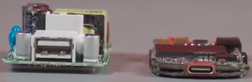
The ACF topology offers the best of both worlds by enabling ZVS operation over the entire line
           and wide load and voltage range. Compared to the traditional QR flyback, the ACF topology
           includes an additional high-side switch and capacitor to slew the switched-node voltage (VSW) to
           the opposite rail during the dead-time and achieve ZVS. MHz-ACF using GaN power ICs was
           demonstrated academically in 2016v and available for industry since the 2018 introduction of TI’s
           UCC2878x ACF PWM controller. GaN enables high frequency ACF operation and results in a
           dramatic size reduction of the transformer, for example from a 22mm-high RM10 bobbin-based
           transformer at 50kHz to an 8mm-thin EI25 planar transformer at 500kHz, as shown in figure 1.

           Fig. 1: How high frequency drives smaller passive components, 50W fast-charger example. On the left,
           ~100 kHz traditional bobbin (22 mm high), on the right, ~500 kHz planar transformer (8 mm).

           Size reduction by increased frequency and pulsed operation (bulk capacitor elimination) led to the
           introduction of OPPO’s ultra-thin 50W ‘Cookie’ GaN-power-IC-based fast charger in 2020. This was
           a perfect example of combining GaN with some novel system partitioning to reduce the converter
           size and profile and ultimately creating a new and unique out-of-the-box user experience.

           High-frequency PFC, without the bridge
           Conventional PFC topologies for mid-power (100-500W) applications include an input bridge
           rectifier followed by a traditional boost converter. As the boost switch is turned on and off at a
           given switching frequency, the switch on and off times are controlled such that the AC line input
           current follows the same shape and phase as the AC line voltage and the DC bus output voltage is
           maintained at a constant level. During 90VAC input and full-load conditions, this circuit can reach
           efficiencies of about 96%. The boost converter itself can be made very efficient but the AC input-
           bridge losses are very high, causing severe thermal extremes and poor overall efficiency.

           Enter the ‘bridgeless totem-pole’ PFC topology.

           In conventional PFC circuits with a standard AC rectifier, at any point in time, two diodes of the
           input bridge are always conducting and generate > 50% of the total PFC circuit losses. Many
           bridgeless PFC circuits have been investigated over the past few decades in attempts to eliminate
           the input bridge rectifier and boost system efficiency but few have made it out of the lab and into
           the mainstream market mainly due to higher complexity and cost. These topologies include classic
           bridgeless, semi-bridgeless, bi-directional bridgeless, and bridgeless totem-pole. Each of these
           topologies has their own set of pros and cons but none of them are the perfect solution.

                                                                                                                  2.

This white paper was published in ASPENCORE's Power Electronics News,
July 2021.
While microcontroller-based designs have been implemented for multi-kW datacenter SMPS,
standby losses have been too high to meet consumer market requirements like DoE Level IV
and Euro CoC Tier 2.
Figure 2: 300W CrCM totem-pole PFC schematic and efficiency data.
With the emergence of new controllers in 2021, the high-frequency CrCM bridgeless totem-pole is
emerging as a popular topology due to low EMI, plus simplified voltage and current sensing by the
controller. Switching speeds can be increased up to 10x, from fixed-frequency 50kHz CCM to
200-500kHz for CrCM totem-pole operation, and GaN’s low output capacitance (COSS) delivers a
cool, high-efficiency result.
High-frequency DC-DC: 6x the power with GaN
For fixed-output voltage converters in the 100W-3000W power range, the downstream DC-DC
converter choice is typically an LLC resonant stage with ~400VDC input. The 400V bus can come
from an upstream PFC stage within an encased AC-DC SMPS, or can be the main distribution rail in
a HVDC installation.
The LLC topology has several benefits that include ZVS operation, high efficiency and high power
density, and the ZVS operation makes this converter an ideal platform for increasing the switching
frequency and reducing the size of the magnetics using a high-speed powertrain.
In the industry-standard (DOSA) quarter-brick form-factor, best-in-class silicon-based designs reach
150W. By using GaN power ICs and increasing the DC-DC switching frequency 3x from 275kHz to
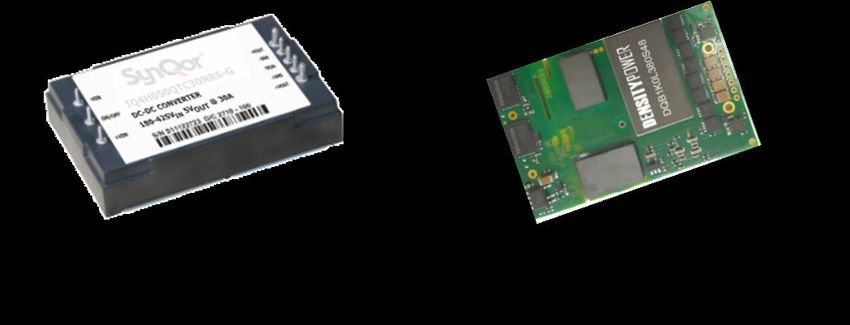
830kHz, the power rating can be increased up to 6x to 1kW.
Figure 3. 400V input DOSA quarter-brick DC-DC converters. On the left, best-in-class Si-based,
275kHz, 150W, and right GaN-based 830kHz reaching 1kW (Density Power).
3.
This white paper was published in ASPENCORE's Power Electronics News,
July 2021.
High-speed GaN enables high-frequency applications
           These are only a few of the vast opportunities in power electronics to be revolutionized by gallium
           nitride power ICs. As operating frequencies are increased and magnetic sizes decreased, the entire
           eco-system will continue to evolve, including upgraded magnetic materials, new planar
           transformer designs, smaller capacitor technologies, new circuit topologies, improved thermal
           materials. The results are higher efficiencies, improved robustness, new power adapter form-
           factors and ultimately, lower costs.

           For More Information:
           iR. Watson, F. C. Lee and G. C. Hua, "Utilization of an active-clamp circuit to achieve soft switching

           in flyback converters," in IEEE Transactions on Power Electronics, vol. 11, no. 1, pp. 162-169, Jan.
           1996, doi:10.1109/63.484429.
           ii D. Kinzer, Navitas “Welcome to the Post-Silicon World: Wide Bandgap Powers Ahead”,
           keynote PCIM 2016.
           iii Gallium nitride (GaN) overview at https://www.navitassemi.com/gallium-nitride-the-next-
           generation-of-power/
           iv D. Kinzer and S. Oliver, "Monolithic HV GaN Power ICs: Performance and application," in IEEE

           Power Electronics Magazine, vol. 3, no. 3, pp. 14-21, Sept. 2016, doi: 10.1109/
           MPEL.2016.2585474.
           v S. Oliver, T. Ribarich, “State-of-the-Art Mobile Charging: Topologies, Technologies and
           Performance”, APEC 2017 , Industrial Session IS05,
           https://www.navitassemi.com/download/state-of-the-art-mobile-charging%ef%bf%bdtopologies-
           technologies-and-performance/?wpdmdl=36540&ind=1561120266242

                                                                                                                    4.

This white paper was published in ASPENCORE's Power Electronics News,
July 2021.
You can also read


