ADVANCES IN ZNO: MANIPULATION OF DEFECTS FOR ENHANCING THEIR TECHNOLOGICAL POTENTIALS - DE GRUYTER
←
→
Page content transcription
If your browser does not render page correctly, please read the page content below

Nanotechnology Reviews 2022; 11: 575–619
Review Article
Irfan Ayoub, Vijay Kumar*, Reza Abolhassani, Rishabh Sehgal, Vishal Sharma,
Rakesh Sehgal, Hendrik C. Swart, and Yogendra Kumar Mishra*
Advances in ZnO: Manipulation of defects for
enhancing their technological potentials
https://doi.org/10.1515/ntrev-2022-0035 an essential part of any research area. The correlations of the
received October 17, 2021; accepted January 3, 2022 microstructural characteristics with electrical and optical
Abstract: This review attempts to compile the physics and properties of ZnO are then a natural step for further facili-
chemistry of defects in zinc oxide (ZnO), at both, the tating an efficient way toward advanced ZnO-based materials
fundamental and application levels. The defects, either and devices. The present review is an effort to shed light on
inherent ones or introduced externally, have broadened the the defects of ZnO, properties, theoretical aspects, and corre-
ZnO material field in various directions. The ZnO material sponding applications.
exhibits many defect-attributed properties leading to broad Keywords: zinc oxide nanomaterials, defects, techno-
technological applications: electronic and optoelectronic logical applications
devices, sensors, optical components, ceramic industry, bio-
medical, catalysis, lightening, etc. Considering the huge
defect-dependent technological scopes, the ZnO material is
constantly engineered for various defects, and corresponding 1 Introduction
functionalities are tailored with respect to particular applica-
tions. The functional properties of ZnO are strongly influ- The word “zinc” has been derived from the Persian word
enced by the defects, and as a result, the defect engineering “sing,” which means stone. Zinc ore has been initially
of the ZnO materials has remained an important motivation used for the fabrication of the copper–zinc alloy, brass,
in materials science and engineering in terms of localized and zinc salts for medicinal uses even before the dis-
defects, extended defects, impurities, and surface defects, covery of zinc as a metal. The materials of brass were
etc. A detailed characterization of these defects seems to be also being used in Babylonia and Assyria around 3000
BC, as well as in Palestine in between 1000 and 1400 BC
approximately. It took centuries for the recognition of
* Corresponding author: Vijay Kumar, Department of Physics, zinc as a metal, and finally, after the reemergence of
National Institute of Technology Srinagar, Srinagar, Jammu and zinc in the seventeenth century, the word “zinc” became
Kashmir – 190006, India; Department of Physics, University of the widely famous. Because zinc exists only in the compound
Free State, P.O. Box 339, Bloemfontein ZA9300, South Africa, form in nature, it has been first extracted from the carbon-
e-mail: vj.physics@gmail.com
ates of the zinc. At the early stage of the evolution of zinc,
* Corresponding author: Yogendra Kumar Mishra, Smart Materials,
NanoSYD, Mads Clausen Institute, University of Southern Denmark,
it was particularly well suited to alloys along with other
Alsion 2, Sønderborg, 6400, Denmark, e-mail: mishra@mci.sdu.dk metals. It was being used initially for the manufacturing
Irfan Ayoub: Department of Physics, National Institute of of coins. One of the primary challenges in extracting
Technology Srinagar, Srinagar, Jammu and Kashmir – 190006, India zinc at the early stages was regarding its propensity of
Reza Abolhassani: Smart Materials, NanoSYD, Mads Clausen vaporization before reaching the melting temperature of
Institute, University of Southern Denmark, Alsion 2, Sønderborg,
more than 1,000°C. For solving the issue, the researchers
6400, Denmark
Rishabh Sehgal: Department of Electrical and Computer condensed the vapors without any exposure to air during
Engineering, University of Texas at Austin, Austin, Texas 78751, USA the smelting process [1]. With the advancement of tech-
Vishal Sharma: Institute of Forensic Science & Criminology, Panjab nology, it has been found that zinc exists in nature
University, Chandigarh, 160014, India only in the compound form, mainly involving oxygen or
Rakesh Sehgal: Department of Mechanical Engineering,
sulfur. Among them, the compound “zinc oxide (ZnO)”
National Institute of Technology Srinagar, Srinagar,
Jammu and Kashmir – 190006, India
was being discovered to be one of the most functional
Hendrik C. Swart: Department of Physics, University of the Free materials with remarkable and unique physical and che-
State, P.O. Box 339, Bloemfontein ZA9300, South Africa mical properties such as strong chemical stability, high
Open Access. © 2022 Irfan Ayoub et al., published by De Gruyter. This work is licensed under the Creative Commons Attribution 4.0
International License.
576 Irfan Ayoub et al.
electrochemical coupling coefficients, a broad spectrum of of 3.37 eV, it possesses higher exciton binding energy than
radiation absorption, along with high photostability [2,3]. In that of GaN, that is, 60 meV at room temperature (RT)
materials science, the ZnO is categorized as a semicon- [6,8,9,11–15], because of which the excitonic emission pro-
ductor of group II–VI, with a covalence lying in-between cesses persist at or even above RT [16,17]. This exceptional
the ionic and covalent semiconductors [4]. characteristic feature makes it a remunerative material for
The thirst and need of the human civilization for RT ultraviolet (UV) lasing devices [5]. It acts as a potential
better living standards has remained the demand in every candidate for application in optoelectronic and spintronic
century. The fulfillment of the demands always relies on devices. The material properties of ZnO make it applicable
the shoulders of the researchers working in the different to a wide range of applications in UV light emitters, varis-
fields. Researchers design different ways to attain the required tors, ceramic positive temperature coefficient thermistors,
properties for any materials of need, such as doping, transparent high-power electronics, surface acoustic wave-
codoping, ion beam radiation, and creating defects. Among guides, piezoelectric transducers, chemical and gas sen-
the diversity of materials and needs, the ZnO, which belongs sing, solar cells, piezoelectric nanogenerators (PNGs), etc.
to the oxide semiconductors, is of great interest. The research [8–10,18–22]. Also, it possesses an important position in
interest in ZnO is exponentially growing as is observed from a solid-state lightning technology because of its high emis-
surge in the number of publications in these materials [5]. The sion efficiency [23]. It opens the opportunities toward the
graph presented in Figure 1(b) is taken from Scopus depicting formation of new optical and magnetic effective devices,
the number of publications per year for the ZnO, from which it such as spin-polarized solar cells [24], spin light-emitting
is clearly evident that after 2017, the number of publications diodes (LEDs) [25], and magneto-optical switches [26]. It
per year is more than 100,000. This surge is due to the non- has been modeled into several nanostructured polymorphic
toxic nature of ZnO and its cost-effective production on both shapes, such as nanorods (NRs), nanowires (NWs), nano-
small and large scales [6,7]. Among the cluster of available flowers, and nanoparticles (NPs) [27–30]. The above men-
semiconductors, ZnO has been readily used for the past tioned benefits of the ZnO make it favorable for the different
decade as an electronic material for numerous applications fields of science and technology. This diversity in applica-
[8,9]. The defect engineering of the ZnO has remained an tions of the ZnO in different fields is depicted in Figure 1(a)
important motivation in materials science research as the taken from the Scopus, representing the applicability of ZnO
fundamental physical and chemical properties of ZnO much in the various domains of science and technology. These
depend on their defect structures. It is because of the complex nanostructures prove to be important for optoelectronic
nature of the defects that ZnO is being discovered and re- devices owing to their large surface-to-volume ratio [31]. A
discovered repeatedly [10–12]. With a direct band-gap value wide range of methods have been used to synthesize ZnO,
Figure 1: (a) Applicability of the ZnO in the different fields of science and technology and (b) number of publications per year related to ZnO.
Advances in ZnO: Enhancing their technological potentials 577
that is, pulsed laser deposition (PLD), vapor–liquid–solid, 2 Different methods for synthesis
metal-organic chemical vapor deposition, molecular beam
epitaxy, hydrothermal aqueous chemical growth, micro-
of ZnO nanostructures
wave-assisted growth, etc. [32–36]. The density of defects
Due to the diverse nature of structures acquired by the
in ZnO directly depends on the growth methods. Sol–gel
ZnO, the interest in knowing the physics and chemistry of
strategies, including aqueous strategy, are effortless, modest,
these structures has increased drastically in recent years.
and easy to use techniques in business use. Although the
These various structures attained by the nanometric ZnO
other previously mentioned strategies yield nanostructures
make it a unique material with diverse set of character-
that are huge from size perspective, they require refined hard-
istics and prospective uses in a variety of nanotechnology
ware and include significant expenses and temperatures that
disciplines. ZnO occurs in one-dimensional (1-D), two-
limit the utilization of different substrates [13]. Modern crystal
dimensional (2-D), and three-dimensional (3-D) struc-
growth methods make it conceivable to develop huge size
tures [4]. 1-D group makes up the largest group, which
ZnO crystals and wafers, which led to the wide modern utili-
includes NRs [61–63], needles [64], helixes, springs and
zation of ZnO with exceptional results [37]. Yet, polycrystal-
rings [65], ribbons [66], tubes [67–69], belts [70], NWs
line, nanocrystalline, or a normal deficient ZnO material
[71–73], and combs [74]. The 2-D structures of ZnO include
shows interesting unique functionalities [23,38–44], which
nanoplate/nanosheet and nanopellets [75,76]. 3-D struc-
is significant from both theoretical and application view-
tures are mainly flowers, dandelion, snowflakes, coni-
points. Such alleged inferior quality (not regarding virtue)
ferous urchin-like, etc. [77–80]. Different techniques to
ZnO offers greater adaptability to be used in gadget applica-
produce various ZnO structures that differ in shape, size,
tions because of the presence of an enormous number of
and spatial arrangements are depicted in Figure 2. A
different imperfection species in such a framework [45].
detailed summary of ZnO obtained by different methods
They can be delivered at a lower cost and by generally simpler
is given below in the Table 1.
methods [46–51]. Along these lines, polycrystalline or nano-
crystalline ZnO has gotten considerably more attention. This
review article mainly focuses on the manipulation of defects
in ZnO for enhancing their technological applications. Because 2.1 Sol–gel method
of the presence of different types of imperfections, ZnO offers
ascend to generally new material attributes [52–54]. Theore- This technique has been prominently used for the fabri-
tical investigations, particularly first-principle computat- cation of the ZnO because of its numerous benefits, such
ions that relies on density functional theory (DFT), have
also made significant contributions for a better under-
standing of the role of local point imperfections and con-
taminations on the accidental n-type conductivity in ZnO
[55–60]. To date, large number of reviews related to ZnO
have been published, but all those are dedicated to some
particular characteristic and application. In this regard,
this is a unique review as it provides an insight into almost
every aspect of the ZnO. This review article consists of dif-
ferent sections, and each section is subsequently divided into
its respective subsections. After a brief introduction, the
second section provides the information on different ways
of synthesizing the ZnO, followed by the third section, which
provides the detailed information related to the structural
aspects of the ZnO. The fourth section deals with the different
properties possessed by ZnO, that is, optical, thermal,
mechanical, etc. In the fifth section, the defects present in
ZnO are presented, wherein the effect of all of the intrinsic
and the extrinsic defects are briefly explained. In the next
section, some general remarks about the defects have been
presented, and the last section deals with the applications of Figure 2: Different synthesis methods used for the development of
ZnO in a variety of scientific and technological domains. different ZnO structures.
Table 1: Summary of different techniques for the fabrication of ZnO
578
S. no. Technique/method Precursors Characteristics and applications Ref.
2
1 Precipitation process Zn(CH3COO)2 and KOH as a solution Particle diameter: 160–500 nm, BET: 4–16 m /g [81]
Zn(CH3COO)2 and (NH4)2CO3 Zincite structure: spherical particles with a diameter of ∼30 nm [82]
Application: used as a photocatalyst in photocatalytic degradation
Zn(NO3)2 Wurtzite structure with particle diameter ∼50 nm [83]
Irfan Ayoub et al.
Application: used in gas sensors
Zn(NO3)2 and NaOH Spherical size particles of around 40 nm [84]
ZnSO4, NH4HCO3, and ethanol Wurtzite structure with crystal size 9–20 nm and particle size [85]
diameter ∼12 nm
Zn(CH3COO)2 with NH3 as an aqueous solution Particles with length ∼150 nm and diameter ∼200 nm [86]
ZnSO4, NH4OH, and NH4HCO3 Particle diameter ∼0.1–1 μm and length ∼60 nm [87]
Micro-sized ZnO powder, NH4HCO3 Hexagonal and wurtzite structure, flower, and rod-like shapes [88]
Zn(CH3COO)2 and NaOH Hexagonal structure with flower shape [89]
Application: antimicrobial activity
2 Sol–gel Zinc acetate dihydrate, C2H2O4, C2H5OH, and CH3OH Zincite structure, particles of rod-like shape with length ∼500 nm and [90]
diameter ∼100 nm
Application: used for decontamination of sarin
Zinc acetate dihydrate, C2H2O4, and C2H5OH Hexagonal wurtzite structure with uniformly spherical shaped particles [91]
Zinc 2-ethylhexonate, ((CH3)4NOH), ethanol, and 2- Crystallites of cylindrical shape with diameter ∼25–30 nm and length [92]
propanol 35–45 nm
Zinc acetate dihydrate, HN(CH2CH2OH)2, and C2H5OH Hexagonal wurtize structure, particles possess the shape of nanotubes [93]
of the order ∼70 nm
3 Solvothermal hydrothermal and ZnCl2 and NaOH Particle morphology: bullet, rod-like (100–200 nm), sheet [94]
microwave techniques (50–200 nm), a polyhedron (200–400 nm), and so on
Zinc acetate (ZA) and sodium hydroxide Spherical shape with particle diameter around 55–110 nm [95]
ZA, zinc nitrate (ZN), lithium hydroxide, potassium Hexagonal wurtize structure with microcrystallites size of the order of [96]
hydroxide, and ammonium hydroxide ∼100 nm to 20 μm
ZA, ammonia, C16H30O4Zn, C2H5OH, and C3H8O Particles possess irregular ends along with holes, an aggregate of [97]
particles have a size of the order of 20–60 nm
Trimethylamine N-oxide, 4-picoline N-oxide, HCl, toluene, Wurtzite structure with particle shape of NRs (40–185 nm) and NPs [98]
and ethylenediamine (24–60 nm)
ZA, ZN, C2H5OH, and imidazolium tetrafluoroborate ionic Hexagonal wurtize structure, hollow microspheres (2–5 μm) with [99]
liquid nanosized particles, NRs (∼20 nm) along with flower-like microspheres
Zinc acetylacetonate, methoxy-ethoxy, and Zincite structure with average crystal size ∼9–13 nm and diameter [100]
–butoxyethanol ∼40–200 nm
Zn(NO3)2 and deionized water Hexagonal wurtize structure with NRs and NW shapes [101]
Application: electronic and optical devices
4 Emulsion Zn(NO3)2 with surfactants Size of grains: cationic surfactants ∼40–50 nm, nonionic surfactants [83]
∼20–50 nm, and anionic surfactants ∼20 nm
(Continued)
Table 1: Continued
S. no. Technique/method Precursors Characteristics and applications Ref.
Zn(C17H33COO)2, NaOH, decane, water, and ethanol Morphology of particles: irregular particle aggregates with a needle, [102]
nearly spherical, and hexagonal shapes, along with spherical and
pseudo spherical aggregates
Zn(CH3COO)2, heptane, and NH4OH Hexagonal structure, spherical shape with particle diameter [103]
∼0.05–0.15 μm
Zn(CH3COO)2, NaOH, KOH along cyclohexane, and Hexagonal structure, particles show morphologies such as solids, [104]
nonionic surfactants ellipsoids, rods, flakes, and so on
Application: used as a photocatalyst
5 Microemulsion Zn(NO3)2, NaOH, heptane, hexanol, and Triton X-100 Hexagonal wurtize structure with particle morphologies such as a [105]
needle (length ∼150–200 nm, diameter ∼55 nm) and nanocolumns
(length ∼80–100 nm, diameter ∼50–80 nm)
Zn(NO3)2, oxalic acid, isooctane, benzene, ethanol, Spherical shape with diameter ∼11.7–12.9 nm and grain size ∼11–13 μm [106]
acetone, methanol, and so on
Zn(CH3COO)2, aerosol OT, glycerol, n-heptane, NaOH, Hexagonal wurtize structure with the spherical shape of the order of [107]
methanol, and chloroform ∼15–24 nm along with some rod shapes of length ∼66–72 nm and
diameter ∼21–28 nm
ZnCl2, Zn(CH3COO)2, heptane, and so on Hexagonal structure with uniformly dispersed particles of size ∼10 nm [108]
6 Other methods Zn(CH3COO)2 with thermal decomposition Uniform size of particles ∼20–30 nm [109]
Zn(NO3)2 with ultrasonic irradiation Hexagonal wurtize structure with NRs and NW shapes [101]
Application: used in electronic and optical devices
ZnCl2, Na2CO3, NaCl with mechanochemical processing, Hexagonal structure with a particle diameter of the order of ∼21–25 nm [110]
and ZnO tetrapods by flame transport method An efficient way for the fabrication of tetrapod-like structures [111,112]
Advances in ZnO: Enhancing their technological potentials
579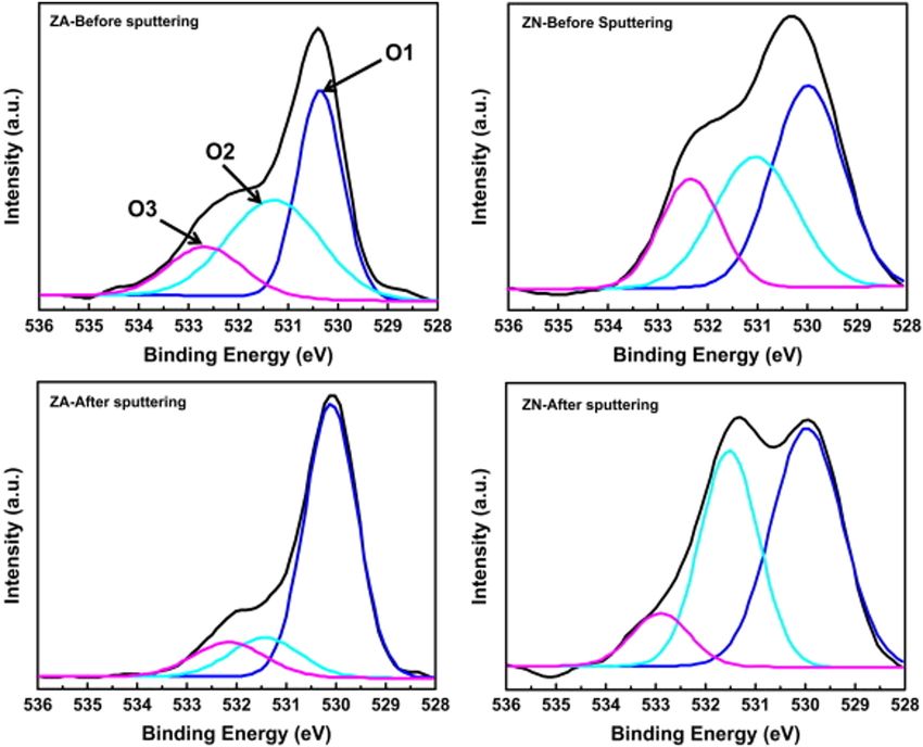
580 Irfan Ayoub et al. as ease of use, low cost, reliability, reproducibility, and the ZnO by using the sol–gel technique. Finally, it is also very mild conditions of synthesis [4]. The efficient optical worth to mention that incorporating the anodic aluminum properties of ZnO NPs attained by this technique have oxide membrane with a sol–gel technique will help to remained a widely known topic of research as is observed synthesize high-quality 1-D nanomaterials along with the due to the surge in the number of scientific publications extension of its applications as a template for the develop- [90]. The basic synthesis procedure for obtaining the films ment of nanostructures. and powder by this method is shown in Figure 3 [113]. Figure 3(a) represents the method of obtaining the thin film from the colloidal sol, and Figure 3(b) illustrates the 2.2 Emulsion or microemulsion method method of obtaining the powder form of ZnO from the col- loidal sol by transforming it into a gel. Benhebal et al. [91] The emulsion is defined as a liquid phase in which synthesized the ZnO powder by utilizing the precursors zinc another discontinuous and immiscible liquid phase is acetate dehydrate and oxalic acid with ethanol as a solvent. dispersed. Emulsions are usually classified based on the The powder form of the ZnO was then characterized using nature of the external phase; one group is called “oil-in- X-ray diffraction, nitrogen adsorption isotherms, scanning water,” and another one is called “water-in-oil.” The electron microscopy, and UV-Vis spectroscopy. It has been terms “oil” and “water” are very well known with their found that the powder possesses the hexagonal wurtzite general definitions as any highly polar hydrophilic liquid structure with spherical-shaped particles. The surface area belongs to the category of “water,” whereas hydrophobic was found to be 10 m2/g by using Brunauer-Emmett-Teller and nonpolar liquids belong to “oil” group [104,105]. (BET) equation. Ristic et al. [92] utilized this method for Vorobyova et al. [102] applied the technique of emulsion obtaining nanocrystalline ZnO. Yue et al. [93] produced for synthesizing the ZnO. They obtained the ZnO by Figure 3: Two examples of synthesis of ZnO by sol–gel method: (a) film of ZnO from colloidal solution and (b) powder form of ZnO from gel. Reproduced with permission from Elsevier [113].
Advances in ZnO: Enhancing their technological potentials 581
performing a reaction between zinc oleate dissolved in dehydrate as a precursor because of its high solubility and
water with sodium hydroxide. The study revealed that decomposition temperature. From the analysis, it has been
processing conditions such as temperature, substrates, observed that the water of crystallization gets lost below
and the ratio of two phase components impact the par- 200°C, and anhydrous ZA starts to develop. Then by slowly
ticle size along with their phases. The obtained ZnO had increasing the temperature up to 400°C both endothermic
different particle shapes such as near-spherical, near- and exothermic reactions take place, which results in the
hexagonal, and spherical aggregates. Lu and Yeh [103] decomposition of the ZA into ZnO and some organic com-
also obtained ZnO by applying the emulsion technique. pounds. Hu et al. [101] suggested the growth of ZnO rods
In a similar fashion, many researchers obtained the ZnO by the sonochemical process and microwave heating.
by the phenomenon of precipitation in an emulsion According to them, ZnO synthesis in this way does not
system. In these systems, ZA is being used as a precursor require any surfactant along with its simple and energy-
along with sodium hydroxide or potassium hydroxide as efficient nature. Also, this method can be used in large
a precipitating agent [104]. Microemulsion are stable and scale with minimum production costs. The ZnO NRs find
isotropic liquids that consist of two different layers along applications in electronics and optoelectronic devices.
with surfactant. It has been observed that the size drop Salman et al. [116] obtained the controlled growth and
on microemulsion is relatively small, lies within the morphology of ZnO in nanostructures by applying the
range 0.0015–0.15 μm [114]. Furthermore, microemulsion domestic microwave synthesis. Grasza et al. [117] obtained
are spontaneous in comparison to the emulsion tech- the pure crystals of ZnO by growing it from a gas phase
nique. Li et al. [105] synthesized the nanometric form of medium, using broad range of values for heating time and
ZnO by microemulsion technique. They obtained the ZnO temperature. They observed that heating in gaseous zinc
by adding the alcohol to the emulsion system which con- results in surface roughness of less than 1 nm, compared to
sists of water, oil, and emulsifier. During the synthesis of the heating in gaseous arsenic, which leads to the dete-
NPs, the exchange process took place among substrates, rioration of the crystal surface. Moreover, by increasing the
microemulsion droplets, and medium in an aggregation temperature and the heating time, improved porosity of
of the formed nuclei. In the whole synthesis process, the surface was observed. The PLD method was used by
different concentrations of the polyethylene glycol 400 Wei et al. [118] for the ZnO fabrication.
were used. Similarly, many researchers have used this
method for the fabrication of ZnO [83,106–108].
In addition to the above-mentioned well-known methods,
there are many other methods to synthesize ZnO such as 3 Structural Informations
pyrolysis spray method, sonochemical method, microwave
method, and developing ZnO from the gas phase. ZnO Structurally, ZnO is mainly found in three different types
nanostructures were prepared from an aqueous solution of unit cells, namely hexagonal wurtzite, zinc blend, and
of ZA (Zn(CH3COO)2.2H2O) and hydrazine hydrate (N2H4) rock salt, as shown in Figure 4 [6,119].
[115]. These precursor solutions were mixed with distilled Among these, the hexagonal wurtzite is well known
water under vigorous stirring while a N2H4 solution was because of its stability at RT and normal atmospheric
added drop-wise into the solution and then transferred pressure [6]. It is composed of triangularly stacked alter-
into a 100 mL Teflon liner and finally subjected to micro- nate biatomic close-packed planes where-in four zinc
wave (Perkin Elmer/Anton Paar Multiwave 3000) oven ions (Zn2+) are located at corners, with oxygen ion (O2−)
irradiation at 150 W microwave power for 10 min. The placed at the center and vice versa. The zinc and oxygen
resulting white precipitate at the bottom of the Teflon ions are thus arranged in the manner of AaBbAaBb…in
was collected, filtered, and then washed several times the direction within a plane [6,12]. The structure
with absolute ethanol and distilled water to remove any of the zinc blend is metastable. Because of its stability,
impurities and then dried. Violet-blue emitting ZnO nano- it is difficult to grow it, as it possesses the stability only
structures were obtained by this method. The electron spin in a cubic structure [6,12]. For stabilization, it is usually
resonance signal was also found to gradually decrease with developed on cubic substrates, such as ZnS [120], GaAs/
increasing annealing temperature signifying the decrease in ZnS [121], and Pt/Ti/SiO2/Si [122], which depicts the com-
the concentration of zinc interstitials (Zni’s) and/or zinc patibility to overcome the innate approach regarding
vacancies (VZn’s) defects in the ZnO nanostructures. Simi- the formation of the wurtzite phase. The symmetry of
larly, Zhao et al. [109] utilized the pyrolysis method and zinc blend structure is given by space group F4̄ 3m in
obtained the ultrapure ZnO particles. They used zinc acetate the Hermann–Mauguin representation and also possess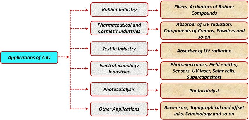
582 Irfan Ayoub et al. Figure 4: (a) The hexagonal wurtzite structure of ZnO, (b) the rock-salt, and (c) zinc blende phases of ZnO. O atoms are shown as white spheres, and Zn atoms are shown as black spheres. Only one-unit cell is illustrated for clarity. Reproduced with permission from Elsevier [119]. two interpenetrating face-centered cubic structure [123]. In material to be suitable for a large number of technolog- contrast to wurtzite, the atoms are arranged in the stacking ical applications [6,13]. The possibility of such utilities order of AaBbCcAaBbCc…within a plane. In the case of has been filled by significant advancement in bulk-crys- rock-salt, both the zinc and oxygen atoms remain sur- tals [37,133] along with the thin-film development in rounded by their six nearest neighboring atoms. It pos- recent years [134–139]. ZnO has a number of character- sesses its stability only at higher pressure (
Advances in ZnO: Enhancing their technological potentials 583
Figure 5: Categorization of properties on the basis of their nature.
regions, including LEDs, laser diodes, and photodetectors order of 0.4 eV. The broad green luminescence possesses
[12,23]. Moreover, the optically lasing action has been noticed its center in between 2.4 and 2.5 eV [150–152]. The phenom-
in ZnO platelets, thin films, a group composed of nanocrystal enon of green luminescence has been observed in samples
of ZnO, and in ZnO NWs [16,17,142,143]. Also, applications synthesized by different methods, it is still not completely
with regard to p–n homojunction have been reported, how- understood whether native defects are the origin of green
ever, security and reproducibility have not been set up yet emission, and if they are, which defects are accountable.
[144–146]. Also the free-exciton binding energy in ZnO is For example, the occurrence of Cu debasements has been
60 meV [16,17], in comparison with 25 meV in GaN [141]. proposed as a possible explanation [153,154], but it has
This huge exciton binding energy shows a proficient exci- been observed that Cu is not present in all the samples of
tonic emission in ZnO and can endure at both room and ZnO that have been studied for the green luminescence.
higher temperatures [16,17]. As the excitonic strength of the Local imperfections have been proposed as an expected
oscillators is significantly greater in comparison to the cause for the mentioned phenomenon. It has been reported
direct electron–hole transitions in direct gap semiconduc- that VZn enhances green luminescence [150,151,155]. For
tors, the enormous exciton binding energy of ZnO makes it the proper explanation of this phenomenon, different inter-
an efficient material for optical gadgets that rely on exci- pretations have been suggested by the researchers. Some
tonic impacts [147]. researchers have recommended that the green luminescence
arises because of the oxygen vacancies (Vo’s) [156–162].
Pramanik et al. [163] have recently investigated the effect
4.2 Optical property of Vo’s on the photoluminescent property of the ZnO. They
observed that with the increase in the synthesis time, both
In general, the visible luminescence arises due to the the band gap and the PL intensity start decreasing. The string
recombination of the deep level defects, that is, so-called green emission has been observed at approximately 540 nm,
deep level emission. These imperfections are generally the whereas blue emission has been observed at 485 nm. They
consequences of several factors, such as crystal perfection, also observed the shift in the emission by changing the band
surface morphology, stoichiometry deviation of the mate- gap excitations. The PL spectra recorded for the samples
rial, and doping and impurities. [148,149]. Because of the synthesized with a slight difference in their preparation
high luminosity in the green–white range of the spectrum, time and the CIE diagram for visualization of the emission
ZnO is, additionally, an efficient material for phosphor colors are shown in Figure 6. Besides different explanations,
applications. The emission spectrum of the ZnO has a some researches have also studied the effect on the emis-
peak at 495 nm and an extremely wide half-width of the sion intensity due to change in the number of the Vo’s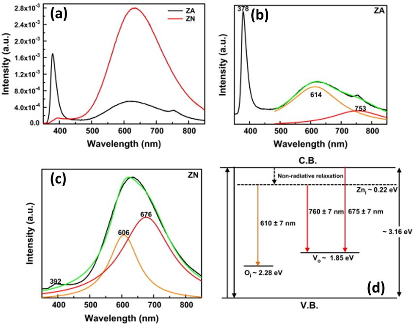
584 Irfan Ayoub et al.
Figure 6: Excitation wavelength-dependent normalized PL spectra corresponding to the samples grown for microwave synthesis time of (a)
1 min, (b) 2 min, and (c) 4 min. Insets show the variation of integrated visible PL intensities as a function of excitation wavelength for all the
samples. (d) Color chromaticity diagram for the sample corresponding to (a). Reproduced with permission from Elsevier [163].
[158,162–164]. Their argument related to the Vo’s availability precursors and urea as a fuel. UV and orange-red light
depends on the perception of a line with g ∼ 1.96 in electron were emitted due to different defects in the NPrs. XPS
paramagnetic resonance (EPR) estimation [158,162]. showed that the O 1s peak consists out of three compo-
In addition, ZnO is a potential material for applica- nents: O1 (ZnO), O2 (deficient oxygen; OH groups), and
tions in vacuum fluorescent displays and field emission O3 (adsorbed species), respectively, as shown in Figure 7.
displays because of its n-type conductivity nature. The The O2 is linked with O2− ions in oxygen-deficient regions
inception of luminescence centers and the luminescence within the matrix of ZnO and/or Zn–OH groups. Hence,
mechanism are not so much comprehended, ascribed to variation in the intensity of this part may be somewhat
Vo’s or Zni’s, with no reasonable proof. Because these linked to the variation in the concentration of oxygen
imperfections cannot transmit in the green regions, it vacancies (Vo). The relative intensity of the O2 peak is
has been proposed that VZn’s are an almost certain reason much higher for the ZN in comparison to ZA sample,
for the green glow. VZn’s are acceptors and prone to form in meaning that the concentration of oxygen defect is higher
n-type ZnO [165]. Kumar et al. [166] with the help of X-ray in the case of the ZN. This effect was confirmed with the
photoelectron spectroscopy (XPS) and PL, demonstrated broad orange-red emission from 500 to 850 nm that was
that the emission from ZnO is directly related to the defects obtained from the ZnO NPr synthesized with the ZN pre-
in the ZnO. ZnO nanophosphors (ZnO NPr) were synthe- cursor. The observed phenomenon may be ascribed to dif-
sized by a combustion method using ZN and ZA as ferent kinds of defects, and a sharp UV band, due to theAdvances in ZnO: Enhancing their technological potentials 585
Figure 7: O 1s XPS peak of ZnO NPs before and after Ar+ sputtering. Reproduced with permission from Elsevier [166].
passivation of defects, at 392 nm from ZnO NPr prepared incredible adaptability for the preparation, planning, and
with the zinc acetate precursor, as shown in Figure 8. A integration of electronic and optoelectronic gadgets [7].
possible schematic energy diagram was drawn from the Also, for the examination of the high power and high tem-
observed data is shown in Figure 8(c). The band transition perature electronic and optoelectronic devices, the thermal
from Zni to Oi level, Zni to Vo level and Vo to valence band conductivity, governed by the contribution of the rotational,
is obtained at ∼2.06, 1.43, and 1.51 eV, respectively. vibrational, along with the electronic degrees of freedom, is
an incredibly essential material characteristic. The phonon–
phonon scattering acts as a limiting mechanism for the
thermal conductivity in pure crystals, which is inversely
4.3 Thermal property
related to temperature. The phonon–phonon Umklapp scat-
tering and phonon scattering by point and extended defects
The characteristic of large thermal conductivity in ZnO has
dominated the heat transmission. Similar to the existence of
made it valuable for an added substance; that is, ZnO
thermal conductivity due to imperfection in other semi-
is added to elastic for the expansion of the thermal con-
conductors, the defects have a crucial role in the thermal
ductivity of tires. High thermal conductivity converts into
conductivity shown by ZnO [168].
enhanced proficiency of heat expulsion amid gadget activity
[167,168]. Besides this, the semiconductor gadget creation
measures incredibly advantage due to the agreeability to
wet chemical etching at low temperature. Furthermore, the 4.4 Mechanical property
studies have revealed that ZnO thin films can be incised
with an acidic, alkaline, and also by a mixture of solutions. In piezoelectric materials, an imparted voltage distorts
This chance of low-temperature chemical etching provides the crystal and vice versa. These materials are commonly586 Irfan Ayoub et al. Figure 8: (a) PL spectra of the different ZnO NPr, (b) and (c) are the deconvoluted peaks of the broad band PL spectra, and (d) schematic energy band diagram of PL spectra. Reproduced with permission from Elsevier [166]. utilized as sensors, transducers, and actuators. The weak have also been performed. The studies confirmed the pre- symmetry of the wurtzite crystal structure joined with sence of oxygen, silicon, zinc, and platinum with 53.98, an enormous electromechanical coupling in ZnO offers 26.48, 17.91, and 18.37%, respectively. ascend to effective piezoelectric and pyroelectric charac- As the piezoelectricity property enables the materials teristics. Piezoelectric ZnO films with consistent thickness to transform the mechanical energy into electrical energy and direction have been developed on various substrates and vice versa, which makes them extremely interesting utilizing distinctive deposition methods, that is, sol–gel, because of solving the energy concern shortly. As a spray pyrolysis, chemical vapor deposition, molecular- result, materials that possess high piezoelectric coeffi- beam epitaxy, etc. [157,169–175]. Because of this piezo- cients are being found as an intriguing study area for electric property offered by the ZnO thin films, they are researchers. In this regard, the ZnO also has gained largely being used in the development of different types increasing focus as a significant semiconductor because of micro electrochemical systems (MEMs). Tao et al. [176] of its large piezoelectric coefficient among the II–VI com- have utilized the ZnO thin film synthesized by using pounds. In comparison to other compounds of the same the sputtering method for the fabrication of two-degree- group (ZnS, CdS, etc.), it has been found that the piezo- of-freedom (2DOF) MEMS piezoelectric-vibration energy electric tensor of ZnO is two times that the rest [177]. At harvester chip. The design procedure they followed for the very first in 1994, Dal Corso et al. [178] used the ab the development of the MEMs is shown in Figure 9. The initio approaches for the evaluation of the piezoelectric fabricated device has been found to possess the piezo- constant of ZnO. According to their calculations, they electric coefficient of the order of 4.66 pc/N. For the con- concluded that the strong piezoelectric behavior is due firmation of the percentage composition of the different to its low clamped-ion contribution. Similarly, Hill and elements, the energy dispersive X-ray spectroscopic studies Waghmare [179] used the first-principle simulations for
Advances in ZnO: Enhancing their technological potentials 587 Figure 9: Procedure for the development of the 2DOF MEMs based on the ZnO. Reproduced with permission from Elsevier [176]. (a) Patterning Pt/Au bottom electrode through a lift-off process, (b) spin-coating photoresist and followed by lithography, (c) deposition of ZnO by sputtering at room temperature, (d) remove photoresist by wet etching, (e) deposition of Pt/Au top electrode, (f) patterning SiO2 by RIE, (g) frontside feature patterning through lithography and DRIE process, and (h) backside feature patterning and realease the structure. the investigation of the effects of stress and temperature key components of their studies were substrate temperature, on the piezoelectric property of ZnO. They observed that optical loss, radio-frequency electrical activity, etc. Von Pre- the piezoelectric constant is substantially influenced by issig and his coworkers [182] developed a novel technique both stress and temperature conditions. This dependence for determining the piezoelectric strength of ZnO thin films on stress and temperature is very critical for future appli- for MEMS application. cations as fine-tuning of piezoelectric characteristics for specific device applications may be accomplished by con- trolling the ZnO lattice constants. Due to rapid progress in 4.5 Magnetic property electronic technology, low-dimensional nanostructures, that is, NWs and nanofilms, have received greater atten- ZnO is currently being investigated for the ferromagnetic tion in recent years due to their potential uses in nano- behavior at RT that has been observed in the pure semi- scale electronics. Immense attention has been diverted conductor. The genesis of this property observed in the toward the ZnO NW as they act as key components in undoped ZnO is still a matter of debate [183–187]. Most of most of the MEMS. It was for the first time in 2006 the researchers have reported that this property arises when first-principle calculations were used for investi- due to the presence of Vo’s in the ZnO [186,188,189]. gating the piezoelectricity of hexagonal (0001) nonpassi- Panigrahy et al. [186] investigated the ferromagnetic vated ZnO NWs with diameters up to 2.8 nm. It has been characteristic of ZnO that possesses different Vo concen- observed that because of the free boundary, ZnO NWs trations and observed the changes by altering the dif- possess a higher effective piezoelectric constant than ferent synthesizing parameters, such as growth time bulk ZnO [180]. Besides the theoretical, experimental stu- and annealing time. They observed a reduction in the dies have also been carried out on the piezoelectric beha- magnetization as the size and the annealing temperature vior of ZnO. Wacogne et al. [181] have investigated the of NRs has been increased, owing due to a decrease in piezoelectric characteristics of ZnO films experimentally. The the defect-related emission from the singly charged Vo.
588 Irfan Ayoub et al.
They conclude that the concentration of the Vo and mag- of the medium and external surface of the microbes, so-
netization are directly interrelated to each other. Xu and called the zeta-potential is altogether influenced by the con-
coworkers [190] recommended that the single charge Vo centration of nanostructures that legitimately influences
positioned close to the surface play an essential function ROS creation [212]. Ongoing research has additionally
in modulating ferromagnetism in undoped ZnO NPs. revealed that the presence of ZnO nanostructures brings
Some researchers have also investigated the antiferromag- about direct associations and efficient bindings to bacterial
netism in undoped ZnO synthesized via the wet chemical cells and can harm the cell membrane, which results in the
technique at an ambient temperature. The investigations death of cells through apoptosis [192,197]. Such type of
have revealed that the magnetic property of the ZnO is research has been broadly revealed by numerous specialists
strongly correlated with the concentration of Vo at the sur- around the world against a few miniature living beings.
face [190]. Furthermore, the antibacterial properties of ZnO nanostruc-
tures, along with their shape, size, and tested micro-organ-
isms was reported by the various researchers [213–224].
4.6 Biomedical property
In the previous years, when contrasted with other metal
oxides, it has been observed that ZnO provides an envir- 4.7 Other properties
onment hostile to bacterial properties, because of which
it acts as a hotbed for the researches. ZnO nanostructures Besides the above-mentioned characteristics features, the
have demonstrated more toxic behavior against microor- exceptional high radiation hardness greater than GaN
ganisms and are less receptive to human cells [191–194], shown by the ZnO is very crucial for different purposes
as in ZnO nanostructures reactive oxygen species (ROS) at high altitudes or in space. Also, it is possible to alter
enables it for the antibacterial action, as it eliminates the the bandgap of ZnO by adding magnesium or cadmium as
bacterial cell [195–199]. The main aim of the ROS is to is done in some GaN-based alloys [225–230]. Furthermore,
prevent humans from infectious diseases and utilize the in comparison with the amorphous silica or organic semi-
technological agents, which are easy to produce, green, conductors ZnO ways out the options for the fabrication of
simply transported, economical, and influenced by bio- thin-film transistors on flexible substrates with enhanced
film morphology, hence proves to be useful for humans electron mobility [231,232]. Other important properties of the
[200,201]. The basic principle of ZnO nanostructures is ZnO are also briefly explained in sections 4.7.1, 4.7.2 and 4.7.3.
dubious yet [202]; however, numerous investigations have
announced the antibacterial systems of ZnO structures
wherein the ROS and response among nanostructures and 4.7.1 Abundance in large single crystals
bacterial cells damages the entire cell and lead to the
freedom of Zn2+ particles [191,195,197,198,203,204]. Most Large single crystals are being fabricated with various methods,
researchers have reported that ROS provides the main comprising hydrothermal growth, vapor-phase transport, and
mechanism of nanotoxicity [195–199,205]. ZnO nanostruc- pressurized melt development [37,133,233–235]. The epitaxial
tures have been accounted as a dominant inhibitor of bac- development of ZnO on local substrates can prompt top-
terial thriving because of ROS creation and release of Zn2+ notch thin films with a decreased level of extended defects.
ions, which harms the cell wall and causes cell death This has been found effective when contrasted with GaN,
[206–209]. Most of the metal oxides act as a suitable anti- for which local substrates do not exist. Considering how
bacterial agent because of ROS production, which results in the GaN-based gadgets have accomplished high efficien-
the formation of O2−, OH−, and H2O2 [205,207]. The antibac- cies irrespective of the moderately huge concentration of
terial proficiency of ZnO nanostructures unequivocally relies expanded imperfections, it is conceivable that a high-
on the size of nanostructures. There is an effective increment quality ZnO-based gadget could outperform the efficien-
in the surface-to-volume proportion as the size of the ZnO cies acquired with GaN [136–139,206,236].
nanostructures diminishes, thus improving the surface area
when contrasted with volume, and ROS creation depends
directly upon the surface area of ZnO nanostructures 4.7.2 Effective surface conductivity
[196,210]. Also, an efficient increase occurs in ROS produc-
tion when the concentration of the ZnO starts rising [211]. The thin films fabricated from ZnO via different methods
Furthermore, the difference between the electrical potential possess a very sensitive nature if their surface getsAdvances in ZnO: Enhancing their technological potentials 589
exposed to gases. It may be used as a low-cost odor from the harmony of the boson-like exciton within the
sensor able to sense the freshness of foods and drinks, nanocrystal [243]. Furthermore, the ZnO crystals and, spe-
owing to its prominent sensitivity to trimethylamine pre- cifically, thin films reveal nonlinear optical activity at the
sent in the odor. The working of the sensor action is not second-and third-order, which has been found useful for
fully understood. Recent investigations uncovered the nonlinear optical gadgets. The nonlinear optical effects in
existence of an electron layer buildup on the surface in ZnO thin films proves to be beneficial for integrating non-
vacuum-tempered single crystal, which vanishes when the linear optical gadgets [245].
material is exposed to encompassing air. This layer may
also assume a function in the sensor activity [237–239].
Recently, the EPR measurements were performed for 5 Native defects in ZnO
proper understanding of the intrinsic defects at different
temperatures. The researchers have observed that the The development of nanotechnology has opened up large
occurrence of the defects on the surface has a significant number of possibilities for manipulating the ZnO struc-
role in conducting the behavior of ZnO. Most interest- tures on all dimensions and broadens its application
ingly, it has been observed that at 300°C, only surface field. Besides some inherent defects that are very much
defects became evident in the EPR spectra of ZnO nano- responsible for the different properties, engineering the
crystals, which eventually favors the p-type conduc- ZnO nanostructures with regulated dimensions, size, por-
tivity [240]. osity, crystal aspects, and mesoscale geometries has greatly
improved their performance for variety of applications
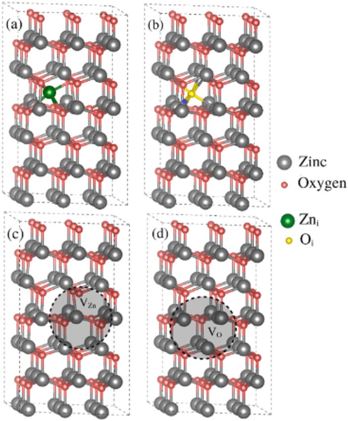
[246,247]. The local or intrinsic or native deformities are
4.7.3 Nonlinear coefficients the blemishes in the crystal lattice that include just the
constituent components [7]. ZnO mainly possesses six types
The linear and nonlinear optical characteristics of any of defects, that is, vacancies, interstitials, and antisites (a
semiconductor are very important from both the theore- “Zn” molecule involving an “O” lattice site or vice-versa),
tical and the experimental point of view [241]. Especially, which are pictorially represented in Figure 10 [8,248]. Defects
the nonlinear optical coefficients are significant factors such as Vo’s have low formation enthalpies in p-type ZnO
for comprehending the physics of nonlinear optical pro- and are therefore expected to form readily [156].
cesses [242]. The unique features shown by the nano- Although they may assume a noteworthy part as
semiconductors in comparison to their bulk equivalents compensating centers, Vo’s and other native point defects
have piqued attracted both the fundamental and the are assumed to be the main cause of the unintentional
technological researchers [243]. The efficiency of the n-type conductivity in ZnO [155]. Discussion regarding
wavelength-conversion devices relies on the nonlinear defects in ZnO primarily concerns their nonstoichiometry
optical coefficients. Among a large number of semicon- and n-type conductivity behavior. In early studies, both
ductors, the appealing nonlinear feature of ZnO has made experimentally and theoretically, it was assumed that
it a good candidate for the nonlinear optical device fabri- only Zni’s and Vo’s are the only defects responsible for
cation. The nonlinear optical characteristics in nanocrys- the above-mentioned property; however, it was unable to
tals have been studied at both the quantum confinement explain many of the other phenomenon [249,250]. Later
effects, that is, weak and strong-confinement regimes. The on, first principle study provides deep insights regarding
theoretical and experimental studies have revealed that the energetics, atomic, and electronic structure of these
the state-filling effect is responsible for the nonlinearity native defects [6,57,59,155,156,251–263]. Most studies have
in the regime of strong confinement. In this regime, the inferred that the Zni has a high arrangement vitality,
state-filling effect acts in such a way that both the photo- although it is a shallow donor. The “O” vacancy has a
excited electrons and hole get independently confined low arrangement vitality, yet it is a profound donor that
[244]. In the case of the weak confinement regime, the cannot produce a high concentration of carrier electrons.
Coulomb interaction in-between the electron and the Subsequently, neither Zni nor Vo is a probable wellspring
hole produces an exciton, which is confined as a quasipar- of n-type conductivity. A few different competitors have
ticle. The size-dependent amplifications of the nonlinear proposed based on the first-principle study: the “H” impurity
susceptibility have also been examined both theoretically unexpectedly incorporated into an interstitial site (OH− – like
and experimentally, and it has been observed that the arrangement) or into the oxygen site [55,264], a metastable
exciton–exciton interactions are mainly responsible for shallow donor for the Vo, a complex of a Zni and “N” con-
the nonlinearity, which in turn leads to the divergence tamination, along with Zni balanced out within the sight of a590 Irfan Ayoub et al.
Figure 10: Different types of defects found in ZnO.
high concentration of the Vo [258,260,265]. Local deformities First-principle counts reliably reveal that the Vo is a
are, by and large, identified with the remuneration of the profound, negative-U contributor, where the 1+ charge
dominating acceptor or donor dopants. For example, it is state is thermodynamically flimsy. It has been observed
simple to create donor defects in p-type material, although that when the Fermi energy is over the “0/2+ level,” the
acceptor defects are simpler to frame in n-type material, imperfection is in the unbiased charge state. When the
every time counteracting the prevailing conductivity. Local Fermi energy is beneath the “0/2+” level, the deformity
deformities have been accepted to play a significantly more has a charge of “ +2e.” The “0/2+” level of the Vo has been
significant function in ZnO, which regularly shows elevated determined to be at 0.5–0.8 eV over the valence-band max-
levels of accidental n-type conductivity. Vo’s and Zni’s have imum [251,255,257,259,271]. Calculations that endeavor to
been frequently conjured as wellsprings of n-type conduc- address the bandgap blunder of the local density approx-
tivity in ZnO [249,266–269]. In general, the native defor- imation assessed the “0/2+” level to be 1–2 eV underneath
mities influence the exhibition of Ohmic and Schottky the conduction-band minimum. The determined movement
contacts. Depth-resolved cathodoluminescence uncovered obstruction for the unbiased Vo is ∼2 eV. Precisely, whether
the arrangement of point defects at metal-ZnO interfaces, oxygen vacancy is primarily accountable for the n-type
prompting modifications in the Schottky barrier character-
istics [270].
5.1 Oxygen vacancies
The oxygen vacancy is among the most referenced defor-
mity in the ZnO literature; it is consequently advantageous
to committing extraordinary consideration regarding this
imperfection. The Vo has been frequently invoked as the
wellspring of accidental n-type conductivity [7]. Even
though the Vo has the most minimal formation energy
among the imperfections that act as donors as depicted
in Figure 11, the calculations performed via computational
methods demonstrate that the Vo is an exceptionally very
deep rather than a shallow benefactor and, thus, cannot
add to an n-type conductivity [57,58,263]. Though the cal- Figure 11: (Color online) Formation energies as a function of Fermi-level
culations available in the published data vary on the position for native point defects in ZnO. Results for Zn-rich and O-rich
conditions are shown. The zero of Fermi level corresponds to the
values for transition levels and formation energies because
valence-band maximum. Only segments corresponding to the lowest-
of the various methods to precise the band gap, they energy charge states are shown. The slope of these segments indicates
solidly agree that oxygen vacancy is a deep donor the charge state. Kinks in the curves indicate transitions between dif-
[57–59,156,251,252,259]. ferent charge states. Reproduced with permission from Elsevier [263].Advances in ZnO: Enhancing their technological potentials 591
conductivity in ZnO has been still unsettled for the past Currently, the majority of the trial examinations of Vo
50 years. For instance, Lany and Zunger [259] anticipated in ZnO have been observed to depend on EPR estimations
groupings of 1017/cm3 or higher, whereas Janotti and Van de [272–279]. Most of these investigations have been sub-
Walle [263] estimated that the formation energy is exces- categorized into two classes, contingent upon the estima-
sively high for noteworthy fixations to exist at balance. One tion of the g-factor: Vo’s with a g-factor estimation of
can comprehend that Vo’s electronic structure in ZnO ∼1.96 to ∼1.99 [272,273,277,278]. There is, nonetheless,
depends on a straightforward model inside molecular overpowering proof that Vo’s are connected with the g
orbital theory (MOT) that includes the four Zn hanging ∼1.99 line [274,275,279]. Similarly, it has been observed
bonds (sp3 hybridization) and two electrons. that illumination is important to have alook at the center,
These Zn hanging bonds join into a completely in line with the outcomes of density-functional calcula-
symmetric “a1” state, which remains in the bandgap, tions wherein suggest that excitation is needed in order to
and three partially degenerate states in the conduction produce the paramagnetic +1 charge state [57,274].
band. In the unbiased charge condition of the Vo, the “a1” Besides this, various authors have also performed
state is doubly involved, and the three states in the con- the EPR studies that have reported the existence of
duction band are unfilled. The control of the “a1” state is one more line at g ∼ 2.004 in the core-shell structures
legitimately identified with the neighborhood cross sec- [240,280–282]. The occurrence of this line has been mainly
tion unwinding around the Vo. In the neutral charge attributed to the surface defects. Researchers, while inves-
express, the four zinc atoms firmly loosen up internal tigating these defects, have revealed that these are posi-
(around the vacancy) by 12% of the balance Zn–O bond tively charged oxygen vacancies that act as deep donors.
length. In the “+1” charge state, they marginally loosen Also, it has been reported that this line becomes visible only
up outward by 3%; and in the “+2” charge state, the four on moving from bulk to the nanodimensions [240,280–282].
zinc atoms unequivocally loosen up outward by 23% as Notwithstanding EPR contemplates, a couple of examina-
shown in Figure 12 [7,57]. The observed significant differ- tions of Vo in ZnO utilizing positron annihilation spectro-
ence in relaxations leads to the decrease in the formation scopy estimations. In these reports, the oxygen samples
energy of different charge states of oxygen such as Vo2 +, Vo0 were electron irradiated and had a Fermi level of 0.2 eV
in comparison to the Vo+. This relative difference in the underneath the conduction band minimum (CBM) after irra-
formation energies results in creating the barrier in which diation. The prevailing remunerating deformity has been
Vo+ is unstable. It is evident from Figure 12(b) and (c) that discovered to be the VZn, along with the other proposals
the amount of the energy required to come out of the +1 regarding the presence of the neutral Vo [283,284]. The
charge state is approximately equal to 0.3 eV [57]. inception of the green glow in ZnO has been a subject of
Figure 12: (a) The atomic relaxations surrounding the oxygen vacancy in different charge states. For each charge state’s equilibrium
configuration, the location of the a1 state is also displayed. (b) Presence of Fermi energy in different charge states at conduction band
minimal. (c) Presence of Fermi energy in different charge states at valence band maximum. Reproduced with permission from Elsevier [57].You can also read