Ab-initio Modeling of Functionalized 2D-Stanene nanostructure in context of FET based Toxic Gas Sensor - IOPscience
←
→
Page content transcription
If your browser does not render page correctly, please read the page content below

IOP Conference Series: Materials Science and Engineering

PAPER • OPEN ACCESS

Ab-initio Modeling of Functionalized 2D-Stanene nanostructure in
context of FET based Toxic Gas Sensor
To cite this article: Swati Verma et al 2021 IOP Conf. Ser.: Mater. Sci. Eng. 1166 012052

View the article online for updates and enhancements.

                               This content was downloaded from IP address 46.4.80.155 on 25/09/2021 at 21:54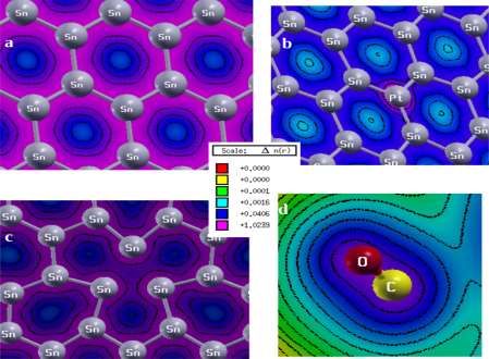
ICMSMT 2021                                                                                                              IOP Publishing
IOP Conf. Series: Materials Science and Engineering              1166 (2021) 012052           doi:10.1088/1757-899X/1166/1/012052

Ab-initio Modeling of Functionalized 2D-Stanene
nanostructure in context of FET based Toxic Gas Sensor

                     Swati Verma1, Arun Kumar2, Hemant Kumar3, Rahul Baghel4, Latika
                     Pinjarkar5, Mohan L Verma6
                     1
                      Department of Electronics & Tele-communication Engineering, FET-SSGI, Shri
                     Shankaracharya Technical Campus, Chhattisgarh, India
                     2
                      Department of Electronics & Tele-communication Engineering, Bhilai Institute of
                     Technology, Durg, Chhattisgarh, India
                     3
                      Center for Basic Sciences, Pt. Ravishankar Shukla University Raipur, Chattisgarh, India
                     4
                      Department of Electrical & Electronics Engineering .FET-SSGI, Shri Shankaracharya
                     Technical Campus Junwani, Chhattisgarh, India
                     5
                      Department of Information & Technology Engineering FET-SSGI, Shri Shankaracharya
                     Technical Campus Junwani, Chhattisgarh, India
                     6
                       Department of Applied Physics FET-SSGI, Shri Shankaracharya Technical Campus Junwani,
                     Chhattisgarh, India

                     Abstract. Detecting toxic gases in the environment cannot be minimized in today’s highly
                     polluted world and the reality of global warming. Carbon monoxide is a highly toxic air
                     pollutant and can cause serious health problems. Sensing materials plays a critical role in the
                     performance of gas sensors. Nanostructure materials exhibit better performance as sensing
                     channels in application for developing novel FET-based sensing devices. In the proposed work,
                     the ab-initio study is performed to explore the performance of 2D-Stanene nano sheet as a
                     sensing substrate for application of field-effect transistors as gas sensor. We explored CO gas-
                     adsorption behaviour on pristine, hole-defective, and Pt-doped Stanene sheet and analyzed
                     structural, charge-density, electronic and transport properties by first principles calculations
                     and exploit its potential for high-performance gas sensing. Here in, to get the measure of
                     sensing properties of Stanene nano sheet after the adsorption of gas molecule, first the
                     molecular model of all the adsorption cases are modelled by considering all possible anchoring
                     sites and optimized, and then calculations were performed based on density functional theory
                     (DFT).

1. Introduction
From the beginning to the end of the day, we continuously sense something and our mind responds
accordingly. We can see, the life of almost every individual across the world depend upon some
automatic gadgets, in which sensor plays an important role[1].

It is interesting to see that sensor is a tool that identifies the existence and behavior of the physical
environment and provides useful information in the form of signals. Due to this property of the sensor,
we can study it at the nanoscale level[2]. Also, various technologies have been developed such as the
nano-electromechanical system, nano-opto-electromechanical system, nano-photonics and the
combination of nanotechnology with microtechnology[3].

              Content from this work may be used under the terms of the Creative Commons Attribution 3.0 licence. Any further distribution
              of this work must maintain attribution to the author(s) and the title of the work, journal citation and DOI.
Published under licence by IOP Publishing Ltd                          1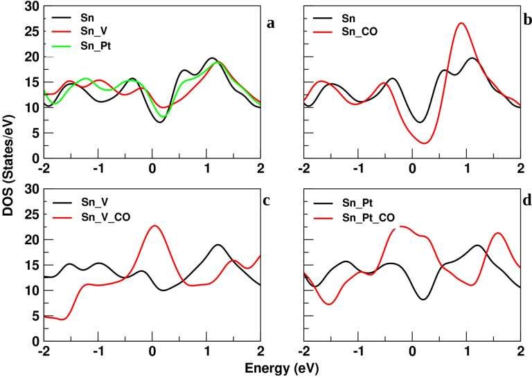
ICMSMT 2021                                                                                     IOP Publishing
IOP Conf. Series: Materials Science and Engineering   1166 (2021) 012052   doi:10.1088/1757-899X/1166/1/012052

Nano-sensors have a wide variety of applications in the field of healthcare, defense, homeland
security, environmental monitoring and light-sensing electronics[4]. We can create more efficient and
effective sensor networks through Tin(Sn) material because of its two-dimensional nature and
excellent electronic and mechanical properties same as Graphene[5]. Sensing materials play a critical
role in the performance of gas sensors.2D nano-materials show much better performance as sensing
channels in application for, sensing channels in application for developing novel FET-based sensing
devices [6-8].

We first modeled a stanene sheet to be used as sensing substrate, to be used as channel of Field-effect
transistors (FETs).Field-effect transistors (FETs) are the kind of transistors that control the flow of
current through the electric field. Field effect transistors (FETs) work on a principle that uses the field
produced by the gate in a way that makes the channel conduct more or less. Here it consists of
terminal, drain and gate where gate manipulates the channel conductivity [9]. The source is a terminal
through which carrier (holes or electrons) enter the channel and drain allow the carriers to leave the
channel. In bipolar transistors, the current that can be carried between the collector and emitter is
modulated by the base current [10].

The working principle of FET sensor is to monitor the conductance change in the gate channel, before
and after the adsorption of target molecules .Motivated by the applicability of 2D Graphene for gas
sensing applications [11-13], we investigated the gas sensing properties of a monolayer of tin as
stanene, in analogy with graphene.

In this work, first-principles methods based on DFT are employed to study the electronic and transport
properties of the pristine, defected and Pt-doped Stanene to exploit its performance as a toxic gas
sensor. It has been reported that functionalization, introducing dopants, and defects can tune the
electronic and magnetic properties of the various nanomaterials[14-16]. Toxic gases are harmful gases
and their reckless intake can cause harm to the respiratory system of the body. Carbon monoxide is an
odorless toxic gas that is formed due to incomplete combustion of carbon and oxygen. Carbon
monoxide is made up of one carbon atom and one oxygen atom with a bond order of 3, where it has
one sigma bond and two pi bonds. It is also known as the invisible killer due to its poisonous nature
and colorless character [17]

2. Computational Details
We exhibit the whole study of based on Density Functional Theory (DFT) which normally using
electron density as a function of space and time. Here, We optimized and concluded all the results
using Kohn-Sham coherent density functional method which further implements on computational
package using open source software Spanish Initiative for Electronic Simulations with Thousands of
Atoms (SIESTA). The SIESTA uses a basis set of strictly-localized atomic orbitals and employs
norm-conserving pseudo potentials .All geometry optimizations and electronic structural calculations
have been performed by using the SIESTA (Spanish Initiative for Electronic Simulations with
Thousands of Atoms) code [18].

Quantum transport theory as implemented in GOLLUM code these codes are based on the density
functional theory (DFT)[19].The exchange and correlation energies are treated within the generalized
gradient approximation (GGA) [20] according to the Perdew-Burke-Ernzerhof (PBE)
parameterization.

Nowadays, Researcher follows the GGA approximation because there are so many advantages over
LDA, Local Density Approximation (LDA) have such limitations it does not account for van der
Waals bonding, not suitable for strongly correlated system and gives a poor description of hydrogen
bonding and over binding error for solids and molecules significantly reduces[21].

                                                         2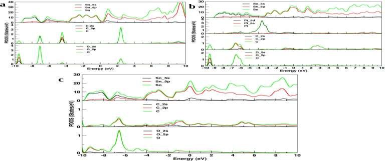
ICMSMT 2021                                                                                     IOP Publishing
IOP Conf. Series: Materials Science and Engineering   1166 (2021) 012052   doi:10.1088/1757-899X/1166/1/012052

Numerical atomic orbital’s (NAOs) with double zeta polarization (DZP) basis set have been used for
geometry optimization. Minimization of energy has been carried out using standard conjugate-gradient
(CG) technique until the forces on each atom are less than 0.005 eV/Å, the mesh cut-off energy is
taken equal to 250 Ry.

3. Results and discussion
3.1 Structural Analysis
To explore the interaction of CO gas molecule with defect fuctionalized stanene systems, we firstly
modeled and optimized the atomic structures of gas molecules and all Stanene systems .We have
considered three sensing substrate system
     1. Sn - the pristine Stanene nanostructure, consisting of 40 Tin (Sn) atoms.
     2. Sn_V- defective Sn system,by creating a vacancy at         center of Stanene nanosheet.
     3. Sn_Pt- doped Sn system,by replacing one Sn atom with dopant Pt atom at center of Stanene
     nanosheet.
We have designed pristine 2D Stanene nano-structure sheet by repeating the unit cell 5 times along Z
direction making it a nanosheet of 40 Tin atoms. After initial relaxation of the pristine sheet the
relaxed lattice constant of a unit cell is 4.647 Å, and the length of Sn-Sn bond is 0.279 nm .These
computed parameters are in good agreement with the previous reported results. After doping of Pt, we
have analyzed the change in atomic structure, bond length between Sn-Sn increases to 0.282 nm and
the bond between Sn-Pt decreases to 0.265 nm, which supports the strong interaction between the
dopant atom and the sheet. In defective Sn system, we have created a vacant space due to creation of
vacancy or hole at the center, the bond length between Sn-Sn decreases to a value of 0.275nm, as
compared to pure stanene sheet.
In figure 1(a) represents the unit cell of Stanene. In figure 1 (b), a pure stanene sheet is formed due to
the repetition of the unit cell of stanene, appearing as a honeycomb-like structure in the 2D plane. In
figure 1(c) one atom of Platinum is doped in the center of the pure Stanene sheet because it provides a
and figure 1 (d) illustrates the two-dimension Sn sheet with a vacant space formed because of the
removal of Sn atom which was at the same place where Pt was doped.

                      (a)                                                           (b)

                        (c)                                                          (d)
  Figure1.(a) 2D unit cell (b) 2D-Stanene 5*5 sheet (c) 2D-Pt doped Sn-sheet (d) 2D-Sn sheet with a vacancy
                       .Dark and white spheres represent Sn and P atoms, respectively.

                                                         3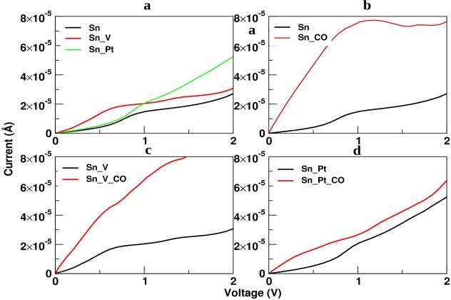
ICMSMT 2021                                                                                     IOP Publishing
IOP Conf. Series: Materials Science and Engineering   1166 (2021) 012052   doi:10.1088/1757-899X/1166/1/012052

After the optimization of CO molecule, the bond length of CO is 0.116 nm, which is in accordance
with the published results.In the case of CO adsorption, there are six possible coordination
configurations depending on the different atoms of CO molecule above three adsorption sites.

         (a)                                             (b)

                                                (c)
Figure 2.(a) Different absorption sites of Stanene sheet (b,c) CO molecules interact with Sn sheet and
                 Sn_Pt sheet with two different orientation at 3 location, respectively

We allow CO molecules to interact with the Stanene sheet in all possible ways and found that there
are three different absorption sites of interaction, which are, i)T-site, on the top of Sn atom (T), ii)C-
site, center of the Sn hexagon (C) in which the molecule is placed in the hollow space region of a
honeycomb-like structure of the sheet., and iii)B-site, the bridge point of a Sn-Sn bond (B),where the
molecule is placed above the bond of the two atoms of Sn-Sn molecules of the sheet. Figure2 (a)
represents the three different adsorption sites. In case of Sn_V sheet, we have placed the molecule on
the vacant site.

                                                         4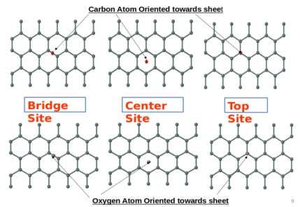
ICMSMT 2021                                                                                     IOP Publishing
IOP Conf. Series: Materials Science and Engineering   1166 (2021) 012052   doi:10.1088/1757-899X/1166/1/012052

The CO molecule has a diatomic structure. Due to the presence of three absorption sites, we can get
six different coordination configurations depending upon the orientation of carbon and oxygen. In
figure 3(b) the CO molecules interact with three different absorption sites, the top row figure shows
the carbon atom orientation, forming a bond with a pure Sn sheet. The down row shows the oxygen
atom orientation, forming a bond with a pure Sn sheet. In figure 3(c) the CO molecules interact with
three different absorption sites, the top row figure shows the carbon atom orientation, making a bond
with pure Platinum, doped in Sn sheet. The down row shows the oxygen atom orientation, forming a
bond with the Platinum, doped in the Sn sheet.

The side view of CO molecules that interacts with three different sheets with pure Sn sheet, Sn sheet
doped with Pt and Sn sheet with vacant space is represent in below figure. When the CO molecules
interact with the pure Sn sheet, it makes two bonds between Sn-O with a bond length of 0.216 nm and
the length of bond between C-O is 0.141 nm. In figure 3(b) oxygen atom of the CO molecule is
bonded with Platinum which is doped in Sn sheet, forming the bond length of 0.248 nm between Pt-O
and the bond length between C-O is 0.12nm. Figure 3(c) represents the vacant Sn sheet where the CO
molecule formed a bond with Sn, having a bond length of 0.258 nm and C-O molecules having a bond
length of 0.127nm.

                                      (a)

                                     (b)

                                    (c)

  Figure 3.Side view of interaction of CO molecules with (a) Pure Sn sheet (b) Sn_Pt sheet (c) Sn_V
                                               sheet
3.2 Charge Density Analysis
Charge Density Analysis plays an important role in determining electronic properties. It gives a clear
description of electron density by explaining the interaction between the atoms of the molecules and
the process of bond formation which helps in predicting the most reactive position for any electron
charge distribution of a molecule. It also provides quantitative information about the different regions
of charge distribution for a molecule. In the charge scale, we can observe a higher electron density at

                                                         5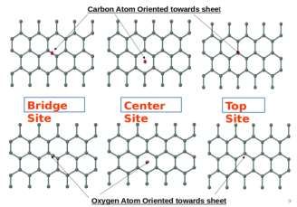
ICMSMT 2021                                                                                     IOP Publishing
IOP Conf. Series: Materials Science and Engineering   1166 (2021) 012052   doi:10.1088/1757-899X/1166/1/012052

the inner-most region (magenta) with a value of +1.0239 and the lowest electron density at the
outermost region (red).
The values of the charge density of colors are given in the center of figure 4. In figure 4(a), the pure
Sn sheet forms a concentric circle in the center of the hexagonal structure of the sheet and the presence
of magenta color, that is visible in the Sn-Sn bond formation region, shows high electron density and
indicates the formation of a strong covalent bond.

Figure 4. The Charge Density Plot of (a) Pure Sn sheet (b) Platinum doped Sn sheet (c) Sn sheet with
                               one atom vacant (d) CO molecules

Figure 4(b), a higher charge density is observed around Platinum atoms of the platinum doped Sn
sheets that means the ionization energy of Platinum (Pt) is higher than Tin(Sn) atom. The formation of
concentric circles around the platinum atoms represents the ionic nature and indicates maximum
charge concentration, which forms magenta circular structures.

In between the Sn-Sn vacant sheet, in figure 4(c), there are concentric circles around the central region
and deformed dumb-bell shapes of the triangular shape formed around the atoms. Hence there is a
partially covalent and ionic bond. From figure 4 (d), it is visible that the CO molecules bond forms the
dumb-bell shape which indicates the sharing of equal charge between atoms and the charge density in
most of the parts are of blue color that shows the presence of the covalent bond.
3.3 Electron Properties Analysis
The forbidden energy gap is the energy difference between the HOMO of the valance band and
LUMO of the conduction band in the density of states (DOS) plotting. In any system, the conduction
band provides enough energy to the electrons which allows them to move freely and this movement of
electrons creates an electric current. The transition of an electron from HOMO of the valance band to
the LUMO of the conduction band is very important to understand the Density of States (DOS) plot
and Projected Density of states (PDOS) plot.DOS plots show the concentration of states for a
particular energy level that an electron can occupy.

                                                         6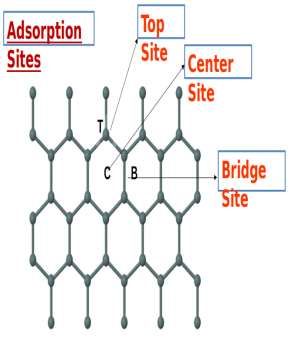
ICMSMT 2021                                                                                     IOP Publishing
IOP Conf. Series: Materials Science and Engineering   1166 (2021) 012052   doi:10.1088/1757-899X/1166/1/012052

In Figure 5(a), the DOS plot shows the variation for all the different types of sheets and their
concentration of states is demonstrated, where the pure Sn sheet has lower peaks in the forbidden gap
region as compared to the vacant Sn (Sn_V) sheet and doped Platinum Sn (Sn_Pt) sheet. On the other
hand, the vacant Sn sheet has higher peaks in the forbidden gap region. On the same figure, continuous
waves are visible, which means that there is no energy gap in all three sheets. At the forbidden energy
region, the sequence for the formation of lower peaks is SnSn_V.
In Figure 5(b) graph represents the DOS plot of pure Sn sheet and pure Sn sheet interacting with CO
(Sn_CO) molecules. In the LUMO or conduction region, the Sn_CO sheet shows high absorbance as
compared to the pure SN sheet. In the forbidden energy gap region, the Sn_CO has a lower peak as
compared to the pure Sn sheet, without interacting with CO molecules which means that the
concentration of electron gets decreases in the region where we interact the CO molecules with the
pure Sn sheet.

In Figure 5(c), the graph represents the DOS plot of the vacant Sn sheet which does not interact with
CO molecules (Sn_V) versus the vacant Sn sheet which interacts with CO molecules (Sn_V_CO). The
forbidden energy gap region of the Sn_V_CO sheet has a higher peak as compared to the Sn_V sheet,
which means that the concentration of electron gets increase in the region when we interact with the
CO molecules with pure SN sheet. In the LUMO or conduction region, Sn_CO interaction with the
sheet shows high absorbance as compared to the pure SN sheet.

                                                         7
ICMSMT 2021 IOP Publishing
IOP Conf. Series: Materials Science and Engineering 1166 (2021) 012052 doi:10.1088/1757-899X/1166/1/012052
In Figure 5, the lower right graph represents the DOS plot of the Platinum doped Sn (Sn_Pt) sheet and
platinum doped Sn sheet interaction with CO (Sn_Pt_CO) molecules. While in the forbidden energy
gap region, the Sn_Pt show a lower concentration of electrons and in the case of Sn_Pt_CO, it shows a
higher concentration of electrons and their antagonistic behavior is visible. The absorbance of CO
molecules through the LUMO band of the Sn_Pt_CO sheet shows high energy after 1.5 eV but in the
case of Sn_Pt sheet, the LUMO band shows the high peak at 1 eV that denotes the acceptance of
electrons in orbital shifting, which means that high energy is required for the bond formation of
Planium and CO molecules. PDOS plots depict the energy of any particular orbitals and the
concentration of states that an electron can occupy.
Figure 6. Projected Density of States with interaction of CO molecule with Sn, Sn_Pt and Sn_V sheet.
In all the three possibilities with the CO molecules (in Figure 6) interaction with sheets of pure Sn
sheet, platinum doped Sn (Sn_Pt) sheet and vacancy Sn sheet there PDOS are shown in figure 6(a,b,c).
In all the cases, the Carbon atom of the CO molecule has shown high absorption in the conduction
band as compared to the oxygen atom when they interact with the sheets.
3.4 Electron Transport Analysis
To study the transport properties of our system, we used the GOLLUM code which is based on the
equilibrium transport theory. GOLLUM code gives the electronic and thermal transport properties of
nanostructured materials. GOLLUM code generates Hamiltonian through Density Functional
Theory(DFT) which corresponds further to generate the S-matrix which gives the physical quantities
such as current by using additional theory in DFT that is equilibrium Green Function (EGF).
The GOLLUM code helps to analyzed and study the first principle behavior of any nanostructure
material through their I-V characteristics by using the DFT-EGF approach.
For transport calculation, the system is divided into three parts that include the left electrode,
nanostructured material (scattering region) and right electrode, which are attached in a consecutive
matter in series to fulfill the valency of each atom. The electrodes which are used for transport analysis
are periodic in structure while the contact nanostructured material is non-periodic in structure.
Figure 7(a), shows the comparative plotting of three different sheets that include pure Sn sheet,
platinum doped Sn (Sn_Pt) sheet and vacant Sn(Sn_V) sheet and these sheets are represented in terms
8ICMSMT 2021 IOP Publishing
IOP Conf. Series: Materials Science and Engineering 1166 (2021) 012052 doi:10.1088/1757-899X/1166/1/012052
of their I-V characteristics. From the graph, it is clear that before the supply of 1V, the output current
in the vacant Sn(Sn_V) sheet shows high peaks as compared to the other two different sheets. After
the supply of 1V, the Platinum doped Sn (Sn_Pt) sheet shows an efficient current with a magnitude
scale of 10-5 Ampere. It can be easily concluded that by adding the functionality to the Sn sheet, in
terms of adding vacancy and dopant Pt atom, we can modulate the conductivity of the sheet. Here,
considerable rise in the current as shown in figure 7(a) indicates the increase in conductivity of our
considered functionalized sheets.
Figure 7. I-V Characteristics with/ without interaction of CO molecules with Sn, Sn_Pt and Sn_V
sheet.
For exploring the adsorption of CO molecule with pure Sn sheet, platinum doped Sn (Sn_Pt) sheet and
vacant Sn(Sn_V) sheet, we have obtained I-V curves which are plotted in figure 7(b),(c),and (d)
respectively. For all the three considered systems, we have compared the I-V curves both in absence
and presence of the adsorbed CO gas molecule. The sharp rise in value of current clearly indicates the
strong interaction between the adsorbed CO gas with the sensing sheets
4. Conclusion
Structural analysis exhibits the variation in adsorption distance relative to system. High peaks in DOS
represents to charge donating nature of adsorbed molecule. Adsorption bond formation nature is found
highly with C atom of CO molecule.
Covalent bonds are formed in Sn hexagonal rings/between C & Sn and partially ionic and covalent
between Pt & Sn.I-V curves exhibit metallic nature with high rise in current with the adsorption of CO
with all considered Sn sheets.
Acknowledgment
Authors are grateful to Chhattisgarh Swami Vivekanand Technical University, Bhilai to grant
financial assistance through TEQIP Project CSVTU/CRP/TEQIP-III/86, dated 05/09/2019, to the
management of Shri Shankaracharya Technical Campus-SSGI to avail research facilities.
9ICMSMT 2021 IOP Publishing
IOP Conf. Series: Materials Science and Engineering 1166 (2021) 012052 doi:10.1088/1757-899X/1166/1/012052
References
[1] Islam, T., Mukhopadhyay, S. C., & Suryadevara, N. K. (2017) “Smart Sensors and Internet of
Things”: A Postgraduate Paper. IEEE Sensors Journal, 17(3), 577–584.
[2] Kanoun, O., & Trankler, H.-R. (2004). “Sensor Technology Advances and Future Trends. IEEE
Transactions on Instrumentation and Measurement”, 53(6), 1497–1501.
[3] Abdel-Karim, R., Reda, Y., & Abdel-Fattah, A. (2020), “Review—Nanostructured Materials-
Based Nanosensors. Journal of The Electrochemical Society”, 167(3)
[4] Patel, S., Park, H., Bonato, P., Chan, L., & Rodgers, M. (2012) “A review of wearable sensors
and systems with application in rehabilitation.” Journal of NeuroEngineering and
Rehabilitation 9(1), 21.
[5] Chen , Z.-W., Shek, C.-H., Wu, C. M. L., & Lai, J. K. L. (2013), “ Recent research situation in tin
dioxide nanomaterials: synthesis, microstructures, and properties. Frontiers of Materials
Science, 7(3), 203–226.
[6] Choudhuri, I., Kumar, S., Mahata, A., Rawat, K. S., & Pathak, B. (2016). “Transition-metal
embedded carbon nitride monolayers: high-temperature ferromagnetism and half-metallicity”.
Nanoscale, (2016), 8(29), 14117–14126.
[7] Şahin, H., Cahangirov, S., Topsakal, M., Bekaroglu, E., Akturk, E., Senger, R. T., & Ciraci, S.
(2009) “Monolayer honeycomb structures of group-IV elements and III-V binary compounds:
First-principles calculations”. Physical Review B80(15).
[8] Miró, P., Audiffred, M., & Heine, T. (2014), “An atlas of two-dimensional materials. Chem. Soc.
Rev.”, 43(18), 6537–6554.
[9] Fortunato, E., Correia, N., Barquinha, P., Costa, C., Pereira, L., Gonçalves, G., & Martins, R.
(2009 “Paper field effect transistor. Zinc Oxide Materials and Devices IV”).
[10] Wise, C. T. A., Suresh, G. R., Palanivelen, M., & Saraswathi, S. “Design of Pentacene based
Organic Field Effect Transistor for low-frequency Operational Transconductance Amplifier”.
Journal of Circuits, Systems and Computers.
[11] Chen, G., Paronyan, T. M., & Harutyunyan, A. R. (2012), “Sub-ppt gas detection with pristine
graphene”. Applied Physics Letters, 101(5), 053119.
[12] Zhu, F., Chen, W., Xu, Y., Gao, C., Guan, D., Liu, C., Jia, J. (2015), “Epitaxial growth of two-
dimensional stanene”. Nature Materials, 14(10), 1020–1025.
[13] Xu, Y., Gan, Z., & Zhang, S.-C. (2014), “Enhanced Thermoelectric Performance and Anomalous
Seebeck Effects in Topological Insulators”. Physical Review Letters, 112(22).
[14] Li, N., Wu, Y.-J., & Liu, Z.-W. (2018), “Determination of baryon-baryon elastic scattering
phase shift from finite volume spectra in elongated boxes”. Physical Review D, 97(1).
[15] Wu, S.-C., Shan, G., & Yan, B. ,(2014), “Prediction of Near-Room-Temperature Quantum
Anomalous Hall Effect on Honeycomb Materials”. Physical Review Letters, 113(25).
[16] Lu, G., Ocola, L. E., & Chen, J. (2009), “Reduced graphene oxide for room-temperature gas
sensors”. Nanotechnology, 20(44), 445502.
[17] Rose , J. J., Wang, L., Xu, Q., McTiernan, C. F., Shiva, S., Tejero, J., & Gladwin, M. T.. (2017),
“Carbon Monoxide Poisoning: Pathogenesis, Management, and Future Directions of Therapy.
American Journal of Respiratory and Critical Care Medicine”, 195(5), 596–606.
[18] http://www.uam.es/siesta
[19] Troullier, N., & Martins, J. L. (1991), “Efficient pseudopotentials for plane-wave calculations”.
Physical Review B, 43(3), 1993–2006.
[20] Perdew, J. P., Burke, K., & Ernzerhof, M. (1996), “Generalized Gradient Approximation Made
Simple”. Physical Review Letters, 77(18), 3865–3868.
[21] Patton, D. C., Pederson, M. R., & Porezag, D. V. (1998), “The Generalized-Gradient
Approximation to Density Functional Theory and Bonding. Frontiers in Materials Modelling
and Design”, 37–50.
10You can also read