A Broadband Low Power CMOS LNA for 3.1-10.6 GHz UWB Receivers

Page created by Marc Hardy
 
CONTINUE READING
A Broadband Low Power CMOS LNA for 3.1-10.6 GHz UWB Receivers
A Broadband Low Power CMOS LNA for 3.1–10.6 GHz UWB
                                                                        Receivers
                                                        Amir Farzad Khavari1                Khalil Mafinezhad2             Mohammad Maymandi Nejad3

                                               1- Ph.D. Candidate, Department of Electrical Engineering, Faculty of Engineering, Ferdowsi University, Mashhad, Iran
                                                                                             amir.khavari@mail.um.ac.ir
                                                      2- Full Professor, Department of Electrical Engineering, Sadjad University of Technology, Mashhad, Iran
                                                                                              khmafinezhad@gmail.com
                                                3- Associate Professor, Department of Electrical Engineering, Faculty of Engineering, Ferdowsi University, Mashhad,
                                                                                                        Iran
                                                                                                maymandi@um.ac.ir

                                               Abstract:
                                               A new approach for designing an ultra wideband (UWB) CMOS low noise amplifier (LNA) is presented. The aim of
                                               this design is to achieve a low noise figure, reasonable power gain and low power consumption in 3.1-10.6 GHz. Also,
                                               the figure of merit (FOM) is significantly improved at 180nm technology compared to the other state-of-the-art designs.
                                               Improved π-network and T-network are used to obtain a high and smooth power gain for the whole frequency band.
                                               Impedance matching and noise matching are designed with double feedback and only one inductor that are used at the
                                               input of the LNA. Post layout simulation is done for design validation. In this design post layout simulations show the
                                               low noise figure of 3.85±0.25 dB, reasonable power gain (18.08dB) and input return loss less than -9.1dB in full band
                                               of UWB. The power consumption of the circuit is only 11.3mW from 1.8V voltage supply. The LNA has the group
                                               delay about 111±43ps. An input third-order intermodulation point (IIP3) of -9.2 dBm is achieved at 4 GHz. The layout
                                               area is 1.056 × 0.658 mm2.

                                                                                                                                                                                                   Journal of Iranian Association of Electrical and Electronics Engineers - Vol.14- No.4 Winter 2017
                                               Keywords: Ultra wideband, UWB, Low Noise Amplifier, LNA, CMOS.

                                               Submission date: 30, April,2015
[ Downloaded from jiaeee.com on 2022-02-22 ]

                                               Conditionally accepted date: 5, Sep., 2015
                                               Acceptance date: 19, Sep., 2016
                                               Corresponding author: Mohammad Maymandi Nejad
                                               Corresponding author’s address: Department of Electrical Engineering, Faculty of Engineering, Ferdowsi University,
                                               Mashhad, Iran.

                                                                                                                 1396 ‫ زﻣﺴﺘﺎن‬-‫ ﺷﻤﺎره ﭼﻬﺎرم‬-‫ ﺳﺎل ﭼﻬﺎردﻫﻢ‬-‫ﻣﺠﻠﻪ اﻧﺠﻤﻦ ﻣﻬﻨﺪﺳﯿﻦ ﺑﺮق و اﻟﮑﺘﺮوﻧﯿﮏ اﯾﺮان‬

                                                                                                         
and excellent IIP3. However distributed amplifiers tend
                                                                                                                                                 1. Introduction                                                                     to consume large dc current due to the distribution of
                                                                                                                                                                                                                                     multiple amplifying stages, which makes them less
                                                                                                                                                 Applications of UWB communication in short-range                                    attractive for low power application. Also, their
                                                                                                                                                 and high speed mobile systems have been popular in                                  demand for high quality transmission lines make them
                                                                                                                                                 academic and industry due to commercialization of the                               unsuitable for low cost application due to the large
                                                                                                                                                 frequency band of 3.1GHz to 10.6GHz by Federal                                      silicon area they need. Another topology is resistive
                                                                                                                                                 Communications Commission (FCC) in 2002 [1].                                        shunt feedback architecture proposed by [5] and [6]
                                                                                                                                                 Since, then there have been many researches on UWB.                                 that provides good wideband matching, higher
                                                                                                                                                     Two methods have been introduced to use the                                     stability, sufficient linearity and flat gain but tend to
                                                                                                                                                 UWB spectrum, i.e. Frequency hopping (FH) scheme                                    suffer from poor noise figure, large power dissipation
                                                                                                                                                 [2] and impulse radio (IR)[3]. In frequency hopping                                 and insufficient power gain. Alternatively, a reactive
                                                                                                                                                 scheme, the UWB band (3.1-10.6 GHz) is divided to                                   feedback implementation provides better noise
                                                                                                                                                 fourteen 528 MHz sub bands with OFDM modulation.                                    performance. The common gate configuration [6] uses
                                                                                                                                                 In impulse radio, transmission of very short pulses is                              the resistive part looking into the source of the
                                                                                                                                                 used with pulse position or polarity modulation.                                    transistor to match the input to well-defined source
                                                                                                                                                     It is possible to have data rates up to 480Mbps in                              impedance (e.g. 50Ω). This topology has the benefit of
                                                                                                                                                 the lower band of UWB (3.1-4.8GHz). Higher data                                     wide bandwidth, good input-output isolation and
                                                                                                                                                 rates can be obtained by using upper band of the UWB.                               linearity, generally independent NF from angular
                                                                                                                                                 Fig. 1 shows the lower band and upper band of UWB                                   frequency over the bandwidth and wideband input
                                                                                                                                                 which consists of band group 1 and 3-5 respectively.                                matching. However, for an input of 50Ω, the required
                                                                                                                                                                                                                                     input transconductance must be 20mS, which translates
                                                                                                                                                                                                                                     into high power consumption. The common gate with
                                                                                                                                                                                                                                     the input matching filter topology can solve this
                                                                                                                                                                                                                                     problem and achieve better wideband property. The
                                                                                                                                                                                                                                     other structure is inductor source degenerated [7] that
                                                                                                                                                                                                                                     employs inductor at source terminal to generate a real
                                                                                                                                                                                                                                     term for the input impedance and often works with
                                                                                                                                                        Fig.1. Band group and frequency limit of UWB                                 cascode transistor. This method due to its good noise
                                                                                                                                                                                                                                     performance, high gain and high reverse isolation, it is
                                                                                                                                                     An ultra wideband (UWB) low noise amplifier                                      usually used in narrowband scheme. Wide band input
                                                                                                                                                 (LNA) for a wireless front-end is crucial in a wide                                 matching is reported with adapting a band pass LC
                                                                                                                                                 range of receiver architectures. The amplifier must                                  filter at the input of the inductor source degenerated
                                                                                                                                                 meet several stringent requirements, such as broadband                              LNA [8]. The band pass filter incorporates the input
                                                                                                                                                 input matching to minimize the return loss, sufficient                              impedance of the cascode as a part of the filter and
                                                                                                                                                 gain to suppress the noise of a mixer, noise match to                               shows good performance while dissipating small
                                                                                                                                                 achieve low noise figure (NF) and enhance receiver                                  amount of dc power. However, the LC filter mandates
                                               Journal of Iranian Association of Electrical and Electronics Engineers Vol14 No.4 Winter 2017

                                                                                                                                                 sensitivity, low power consumption to increase battery                              a number of reactive elements, which could lead to a
                                                                                                                                                 life, high linearity to have high dynamic range and low                             larger chip area and NF degradation due to low Quality
                                                                                                                                                 output intermodulation distortion in high power input                               factor of inductors of LC filter. In this method on-chip
                                                                                                                                                 and small die area to reduce the cost.                                              transformer matching could save some area [9].
                                                                                                                                                     The paper is organized as follows. Section 2                                    Differential amplifiers show excellent treatment toward
                                                                                                                                                 describes the recent design of common ultra wideband                                second order harmonics. These LNAs, however
                                                                                                                                                 LNA topologies, namely, common-gate, resistive shunt                                consume extra power likely about two times of their
                                                                                                                                                 feedback, distributed amplifier and current reuse.                                  single-ended counterpart [10]. Current reuse technique
                                                                                                                                                 Section 3 introduces the widening technique and noise-                              has been used in many recent LNA topologies to
                                                                                                                                                 canceling followed by the proposed circuit topology. In                             reduce power dissipation especially in mobile devices
[ Downloaded from jiaeee.com on 2022-02-22 ]

                                                                                                                                                 Section 4, analytical equations are derived to show the                             [11]. This topology composed of two common source
                                                                                                                                                 gain performance. In Section 5, the noise analysis,                                 configuration stages under common current structure.
                                                                                                                                                 considering the NF at all frequencies is coming. Circuit                            This method effectively save power but its chip area is
                                                                                                                                                 design and post layout simulation results for proposed                              large due to using several inductors. Another solution
                                                                                                                                                 ultra wideband LNA are reported in Section 6. Finally,                              for UWB LNA is to use forward body biasing for
                                                                                                                                                 Section 7 presents the conclusion.                                                  reducing threshold voltage of CMOS transistor [12].
                                                                                                                                                                                                                                     This technique needs low voltage supply; its power
                                                                                                                                                 2. Recent Research                                                                  consumption is very low and is very suitable for low
                                                                                                                                                 Different topology of ultra wideband (UWB) CMOS                                     power application. However, using resistor in body
                                                                                                                                                 low noise amplifiers (LNAs) have been proposed in                                   terminal for limiting the current makes poor noise
                                                                                                                                                 literatures in the last decade: e.g. distributed amplifiers                         performance and the linearity of this method is slightly
                                                                                                                                                 [4] (DAs) provide good impedance matching, flat gain                                worse than that of the other designs.
                                                                                                                                                 and good group delay over a wide range of frequency

                                                                                                                                               1396 ‫ زﻣﺴﺘﺎن‬-‫ ﺷﻤﺎره ﭼﻬﺎرم‬-‫ ﺳﺎل ﭼﻬﺎردﻫﻢ‬-‫ﻣﺠﻠﻪ اﻧﺠﻤﻦ ﻣﻬﻨﺪﺳﯿﻦ ﺑﺮق و اﻟﮑﺘﺮوﻧﯿﮏ اﯾﺮان‬

                                                                                                                                                                                                                                 
In this work, we propose a figure of merit (FOM)         LNA is the large group delay variation that the signal
                                               which takes into account power consumption, noise            can experience, due to several resonances in the input
                                               figure, power gain and bandwidth. Due to the input           matching network. Moreover, it requires moderate to
                                               inductor and the double feedback at input, reasonable        large silicon area and introduces high insertion loss at
                                               input impedance and noise matching could be achieved         input network due to limited quality factor of inductors
                                               at all over the UWB frequencies. Middle stage could be       and degrades the amplifier noise figure (NF).
                                               used for bandwidth gain improvement. Output                  Reference [23] shows improvement the operation of
                                               impedance matching is done with buffer stage. It             UWB receiver by compensation method and using
                                               matches the circuit with standard 50 Ω resistor.             pre-filter, significantly. Also, we have restriction in
                                               Moreover, the high frequency noise can be effectively        using additional filter.
                                               suppressed by the good noise match at input transistor           Another method for increasing the bandwidth of a
                                               with size of transistor, input inductor and double           narrow band amplifier for UWB application is
                                               feedback network. This leads to proper noise figure.         feedback solution. The feedback network could be
                                               The cascode topology results in good isolation of            inductive [15], resistive [16] or parallel resistive-
                                               output from input and has a wideband behavior.               capacitive [17]. The feedback could widen the
                                                                                                            bandwidth of LNA and improves the stability
                                               3. Circuit Analysis                                          especially at high frequency. Furthermore, the precise
                                                                                                            design with double feedback network could give
                                               Fig. 2 shows a typical narrowband cascode LNA                advantage of matching circuit with less inductor at the
                                               topology with inductive source degeneration. In this         input. We must mention that the on-chip inductor has
                                               topology, the inductors Ls and Lg are added for              low quality factor that could degrades the noise figure
                                               simultaneous noise matching and input impedance              of LNA.
                                               matching. [13].                                                  The proposed UWB CMOS LNA used from two
                                                                              Vdd                           feedback network, resistive and capacitive–resistive, as
                                                                                                            shown in Fig. 4. The main advantage in our circuit is
                                                                                                            the low power consumption that makes it suitable for
                                                                                        ZL                  portable devices. The low noise figure of the circuit at
                                                                        Vbias                               all UWB could be done without high current in first
                                                                                       M2                   stage.
                                                                            Lg
                                                                RS                     M1                                                VDD
                                                                                                                                   Rd1                                        VD
                                                                                                                                                      VDD
                                                                                                                                           L3
                                                                                        Ls                                       L1                                            D
                                                                                                                                                  Rd2           L4       Rb2
                                                                                                                                 L2       Cc1
                                                                Fig. 2. Narrowband Cascode Source                                                         Cc2

                                                                                                                                                                                                Journal of Iranian Association of Electrical and Electronics Engineers - Vol.14- No.4 Winter 2017
                                                                                                                                          Rb1        M3                        OUT
                                                                    Degenerated LNA Topology                                 vb1                                       M4
                                                                                                                                         M2
                                                                                                                                                  vb2                 Ibias
                                                  Widening the bandwidth and wideband impedance                    RF2
                                               and noise matching with the source-degenerated UWB                               RF1       Lds
                                                                                                                   CF2
                                               CMOS LNA topology can be done in several ways.                IN
                                               Fig. 3 shows the multi-section LC network and                                             M1
                                                                                                                    Lg
                                               feedback solution.
                                                                                                                       Fig. 4. Proposed UWB LNA
                                                                      out
                                                                                 Feedback
                                                     MultiSection                            out                Double feedback with only one inductor at input
[ Downloaded from jiaeee.com on 2022-02-22 ]

                                                     LC Network
                                                in
                                                                                 in                         transistor is used to have wideband input impedance
                                                                      Ls
                                                                                                            matching. This simple impedance matching network
                                                         (a)                          (b)
                                                                                                            could improve the power consumption and noise figure
                                                                                                            compare to the other UWB impedance matching
                                                         Fig. 3. (a) Multisection LC network for
                                                                                                            topologies.
                                                         wideband input matching (b) Feedback
                                                         network for wideband input matching
                                                                                                                The π-section and T-section improve the power
                                                                                                            gain in cascode structure. The cascode topology is used
                                                                                                            to widen the bandwidth and provides good isolation of
                                                   In LC network, overall imaginary input reactance
                                                                                                            output from input. The power gain of this amplifier at
                                               resonates over the bandwidth. In [7] two section on-
                                                                                                            higher frequencies is also degraded due to the
                                               chip LC chebyshev filter for ultra wideband impedance
                                                                                                            capacitive effect of large size M1 and M2. To
                                               matching is used. In [14] and [8] a three and two
                                                                                                            counterbalance this gain degradation, a series-peaking
                                               section LC filter is used as input reactive network,
                                                                                                            inductor L2 as shown in Fig. 4 is added to make the
                                               respectively. A drawback of this approach for UWB

                                                                                                              1396 ‫ زﻣﺴﺘﺎن‬-‫ ﺷﻤﺎره ﭼﻬﺎرم‬-‫ ﺳﺎل ﭼﻬﺎردﻫﻢ‬-‫ﻣﺠﻠﻪ اﻧﺠﻤﻦ ﻣﻬﻨﺪﺳﯿﻦ ﺑﺮق و اﻟﮑﺘﺮوﻧﯿﮏ اﯾﺮان‬

                                                                                                        
power gain improves at upper edge of UWB. The                                           In (2), ZL is the standard impedance (50Ω) parallel
                                                                                                                                                 inductor L2 could also resonate with Cd2. The Cd2 is                                with rds4 and Zbias. The value of rds4 and Zbias is much
                                                                                                                                                 parasitic capacitor at drain of M2. Cd2 is parallel                                 greater than ZL. Also the capacitor of gate-source (Cgs4)
                                                                                                                                                 combination of gate-drain capacitor (Cgd2) and drain-                               is in femtofarad range, so in UWB frequencies the
                                                                                                                                                 bulk capacitor (Cdb2) of M2.                                                        buffer voltage gain is about 0.5.
                                                                                                                                                     The LNA consists of two transistors as cascode                                      Middle stage with transistor M3 is used for gain and
                                                                                                                                                 (M1, M2), a gain stage (M3) and a buffer stage (M4).                                bandwidth improvement and its effect on the gain of
                                                                                                                                                 The inductor, Lg, beside gate-source capacitor of M1                                the circuit is very crucial. Voltage gain from gate of
                                                                                                                                                 (Cgs1) and double feedback (RF1, CF2RF2) are used for                               transistor M3 to gate of transistor M4 is shown in (3).
                                                                                                                                                 wide band input impedance matching and noise
                                                                                                                                                 matching of the circuit. Rd1 and L1 make shunt peaking                                                                             ଵା௓ ௚
                                                                                                                                                 technique in drain of transistor M2 that improves the                                     െ݃௠ଷ ቆܴௗଶ ൬ܼ௅ െ ݆ ఠሺ஼ ಽା஼೘ర ሻ൰ቇ
                                                                                                                                                                                                                                     ‫ݒ‬௚ସ                        ೒ೞర  ೒್ర
                                                                                                                                                 bandwidth of LNA. The T-section inductor, L1, L2 and                                    ൌ                                                                               (3)
                                                                                                                                                                                                                                     ‫ݒ‬௚ଷ ܴ ൅ ܼ ൅ ݆ ൬߱‫ ܮ‬െ ଵା௓ಽ ௚೘ర ൰
                                                                                                                                                 L3 makes double series peaking technique to improve                                        ௗଶ   ௅        ସ   ఠሺ஼ ା஼     ሻ               ೒ೞర     ೒್ర
                                                                                                                                                 the gain and bandwidth. Also Lds beside parasitic
                                                                                                                                                 capacitor at drain of M1 and source of M2 makes a π-
                                                                                                                                                                                                                                         In (3), gm3 is the transconductance of transistor M3.
                                                                                                                                                 section that improves the bandwidth of LNA. The
                                                                                                                                                                                                                                     Series peaking is used to improve the bandwidth.
                                                                                                                                                 common source transistor (M3) is used for improve the
                                                                                                                                                                                                                                     Inductor       L4       resonates     with       capacitor
                                                                                                                                                 gain. The inductor L4 resonate with Cgs4 (gate-source
                                                                                                                                                                                                                                     (Cgs4+Cgb4)/(1+gm4ZL) .
                                                                                                                                                 capacitor of M4) and Cc2 to improve the bandwidth.
                                                                                                                                                                                                                                         The next gain is vg3/vd2, that could be derived as
                                                                                                                                                 Finally, the transistor M4 is used to make a buffer stage
                                                                                                                                                                                                                                     (4). In (4), Zib is input impedance of gain-stage (M3)
                                                                                                                                                 for output impedance match up to 50Ω, standard
                                                                                                                                                                                                                                     and        is       about        to      1/(ŒɘCg3)=1/[Œɘ
                                                                                                                                                 resistor. In addition to the point of self-biasing of RF1,
                                                                                                                                                                                                                                     (Cgs3+Cgb3+(1+A)Cgd3)]. Cg3 and Cgd3 are total capacitor
                                                                                                                                                 the feedback resistors RF1 and CF2RF2 are also
                                                                                                                                                                                                                                     at gate and capacitor of gate-drain of transistor M3. The
                                                                                                                                                 beneficial for the input impedance matching. Also, the
                                                                                                                                                                                                                                     A is voltage gain between drain to gate of transistor
                                                                                                                                                 feedback resistors RF1 and RF2 are used to have better
                                                                                                                                                                                                                                     M3.
                                                                                                                                                 input impedance matching over wide band and more
                                                                                                                                                                                                                                         Equation (4) shows a shunt peaking technique. The
                                                                                                                                                 stability.
                                                                                                                                                                                                                                     gain roll-off is compensated by Rd1 and L1. Moreover,
                                                                                                                                                                                                                                     it shows double series peaking technique that Cg3
                                                                                                                                                 4. Gain Analysis                                                                    makes two spurious resonances with inductors Leff and
                                                                                                                                                 In the output, the transistor M4 is used as a buffer that                           L2+L3, respectively. Leff is (L1L2+L2L3+L1L3)/(L1+L2).
                                                                                                                                                 also brings us output matching over ultra wideband                                  In the other word we use triple series peaking
                                                                                                                                                 frequency. The output impedance of the circuit could                                technique to increase the bandwidth of the amplifier
                                                                                                                                                 be written as (1).                                                                  and improve the power gain.
                                                                                                                                                                                                                                         The current that flows from the M1 should transfer
                                                                                                                                                                            ͳ                                                        to output. For calculation the is2/id1 we must see the
                                                                                                                                                 ܼ௢ ൎ                                        ଵ                        (1)
                                                                                                                                                        ݃௠ସ ൅ ݆߱൫‫ܥ‬௚௦ସ ൅ ‫ܥ‬௚௕ସ ൯ ൅                                                     parasitic capacitor at the drain of M1 (Cd1) and source
                                               Journal of Iranian Association of Electrical and Electronics Engineers Vol14 No.4 Winter 2017

                                                                                                                                                                                           ௓್೔ೌೞ
                                                                                                                                                                                                                                     of M2(Cs2). is2 and id1 are source current of transistor
                                                                                                                                                                                                                                     M2 and drain current of transistor M1, respectively.
                                                                                                                                                      The gm4, Cgs4 and Cgb4 are the transconductance,
                                                                                                                                                                                                                                     Parasitic capacitor Cs2 is parallel combination of Cgs2
                                                                                                                                                 gate-source capacitor and gate-bulk capacitor of
                                                                                                                                                                                                                                     and Csb2. Cgs2 and Csb2 are source-gate and source-bulk
                                                                                                                                                 transistor M4, respectively. Also Zbias is impedance of
                                                                                                                                                                                                                                     capacitor of transistor M2, respectively. Also, Cd1 is
                                                                                                                                                 Ibias. Ibias is made of a single transistor (M5), so Zbias is
                                                                                                                                                                                                                                     parallel combination of Cgd1 and Cdb1. Cgd1 and Cdb1 are
                                                                                                                                                 equal to (1/jwCgd5)||(rds5). Cgd5 and rds5 are gate-drain
                                                                                                                                                                                                                                     gate-drain and drain-bulk capacitor of transistor M1,
                                                                                                                                                 capacitor and drain-source resistor of transistor M5
                                                                                                                                                                                                                                     respectively. Cd1 and Cs2 provides additional path for
                                                                                                                                                 respectively. We could choose appropriate M4
                                                                                                                                                                                                                                     current signal to the ground and degrade the broadband
                                                                                                                                                 dimension to have output impedance matching. The
                                                                                                                                                                                                                                     performance of the LNA. Lds, Cd1 and Cs2 form a
[ Downloaded from jiaeee.com on 2022-02-22 ]

                                                                                                                                                 buffer voltage gain can be written as (2):
                                                                                                                                                                                                                                     broadband π-section LC network as Fig.5.

                                                                                                                                                 ‫ݒ‬௢    ܼ௅ ቀ݃௠ସ ൅ ݆߱൫‫ܥ‬௚௦ସ ൅ ‫ܥ‬௚௕ସ ൯ቁ                                                   ‫ݒ‬௚ଷ
                                                                                                                                                    ൎ                                                                 (2)            ‫ݒ‬ௗଶ                                                                                       (4)
                                                                                                                                                 ‫ݒ‬௚ସ ܼ ቀ݃ ൅ ݆߱൫‫ ܥ‬൅ ‫ ܥ‬൯ቁ ൅ ͳ                                                                                              ܴௗଵ ൅ ݆߱‫ܮ‬ଵ
                                                                                                                                                      ௅   ௠ସ       ௚௦ସ    ௚௕ସ                                                        ൌ
                                                                                                                                                                                                                                         ܴௗଵ ൣͳ െ ߱ ଶ ‫ܥ‬௚ଷ ሺ‫ܮ‬ଶ ൅ ‫ܮ‬ଷ ሻ൧ ൅ ݆߱ൣ‫ܮ‬ଶ ൅ ‫ܮ‬ଵ െ ߱ ଶ ‫ܥ‬௚ଷ ሺ‫ܮ‬ଵ ‫ܮ‬ଶ ൅ ‫ܮ‬ଶ ‫ܮ‬ଷ ൅ ‫ܮ‬ଵ ‫ܮ‬ଷ ሻ൧

                                                                                                                                                                                                                                        In another word, for improvement in power gain
                                                                                                                                                                      id1       Lds is2                                              and bandwidth, inductor Lds is added between the drain
                                                                                                                                                                                                   1/gm2
                                                                                                                                                                                                                                     of M1 and source of M2. With precise design, Lds, Cs2
                                                                                                                                                                  Cd1                       Cs2                                      and Cd1 will resonate in lower edge frequency of desire
                                                                                                                                                                                                                                     band [18]. Equation (5) shows the relation between is2
                                                                                                                                                 Fig. 5. broadband π-section between Transistors M1                                  and id1:
                                                                                                                                                 and M2

                                                                                                                                               1396 ‫ زﻣﺴﺘﺎن‬-‫ ﺷﻤﺎره ﭼﻬﺎرم‬-‫ ﺳﺎل ﭼﻬﺎردﻫﻢ‬-‫ﻣﺠﻠﻪ اﻧﺠﻤﻦ ﻣﻬﻨﺪﺳﯿﻦ ﺑﺮق و اﻟﮑﺘﺮوﻧﯿﮏ اﯾﺮان‬

                                                                                                                                                                                                                                 
݅௦ଶ                                                                                       the narrowband LNA can be converted into a ultra
                                               ݅ௗଵ                                                                                       wideband amplifier by the proper selection of feedback
                                                                  ሺ݆߱‫ܥ‬௦ଶ ൅ ݃௠ଶ ሻȀሺ‫ܥ‬ௗଵ ൅ ‫ܥ‬௦ଶ ሻ                                  (5)       network. The feedback resistors also provide its
                                               ൌ                                             ௚೘మ
                                                    ݆߱ሾͳ െ ߱ ଶ ‫ܮ‬ௗ௦ ሺ‫ܥ‬ௗଵ ȁȁ‫ܥ‬௦ଶ ሻሿ ൅                    ሾͳ െ ߱ ଶ ‫ܮ‬ௗ௦ ‫ܥ‬ௗଵ ሿ                 conventional roles of flattening the gain over a wider
                                                                                           ஼೏భ ା஼ೞమ
                                                                                                                                         bandwidth with much smaller noise figure degradation.
                                                                                                                                         Depending on the required bandwidth and noise
                                                    In (5), gm2 is the transconductance of transistor M2.                                contribution, the feedback resistor is chosen. Also
                                               To derive the transconductance of the first stage,                                        smaller feedback resistor makes smaller quality factor
                                               (id1/vgs1), we must notice that the input network                                         and more bandwidth and better input impedance
                                               impedance is about to Rs over the wide bandwidth.                                         matching as (8). Although noise calculations will show
                                               Feedback resistors (RF1 and RF2) bring us more                                            us inverse relation between noise figure and the value
                                               bandwidth and wideband matching against the                                               of feedback resistors, we need compromise between
                                               frequencies of 3.1GHz to 10.6GHz.                                                         noise and gain with input return loss and bandwidth.
                                                                                          1/gm2
                                                                                                       Lds
                                                                                             RF1                                                                      RF1/(1+gm1/gm2)
                                                                         Zin
                                                                       Rs       Lg
                                                                                                                                                               Rs Lg
                                                                                                      M1
                                                                                 ZF2
                                                                       Vin                                                                                           RF2           Cgs1
                                                                                            Zx

                                                           Fig. 6. Equivalent circuit at input stage
                                                                                                                                           Fig. 7. Equivalent circuit for Q-factor calculation
                                                   We can write the relation between drain current of
                                               transistor M1 and input voltage source with regard to
                                               Fig.6 and pretty large value of RF1 and RF2. We must                                      5. Noise Analysis
                                               mention that ZF2=RF2/(1-Avc), which Avc is the voltage                                    The main source of noise that increases the noise figure
                                               gain between gate of M1 and drain of M2. After some                                       of a circuit is the first stage. So, to have a glance at
                                               calculation we would have:                                                                noise figure of a circuit, we could analysis the noise of
                                                                                                                                         the first stage. In this section we analyze the noise
                                               ݅ௗଵ              ሺܼ௫ ȁȁܼிଶ ሻ                                              (6)
                                                   ൎ ݃௠ଵ                                                                                 figure of resistive shunt feedback in the first stage of
                                               ‫ݒ‬௜௡       ሺܼ௫ ȁȁܼிଶ ሻ ൅ ‫ܮݏ‬௚ଵ ൅ ܴ௦
                                                                                                                                         CS LNA (Fig. 4) for three main sources of noise in this
                                                                                                                                         structure. To simplify the calculations, transistor is
                                                  In (6) Zx is the input impedance form gate of M1. Zx                                   assumed to have infinite output impedance. Beside the
                                               could be written as (7):                                                                  thermal noise of RF1, RF2 (shunt feedback resistors), the
                                               ܼ௫                                                                                        drain noise current, due to the carrier thermal agitation

                                                                                                                                                                                                                             Journal of Iranian Association of Electrical and Electronics Engineers - Vol.14- No.4 Winter 2017
                                                             ͳ               ͳ ൅ ݃௠ଶ ܴிଵ    ͳ                                            in the channel and the induced gate noise, because of
                                               ൌ                         ȁȁ ቌ            ȁȁ                                              the coupling of the fluctuating channel charge into the
                                                    ݆߱൫‫ܥ‬௚௕ଵ ൅ ‫ܥ‬௚௦ଵ ൯          ݃௠ଶ ൅ ݃௠ଵ ݆߱ ௚೘భ ௅೏ೞ
                                                                                                           ோಷభ ା௚೘మ                      gate terminal are taken into account.
                                                    ͳ       ݃௠ଶ                                                          (7)                 The induced gate noise, drain noise and resistor
                                               ൅       ȁȁ݆߱     ‫ ܮ‬ቍ                                                                      noise power spectral densities are formulated as
                                                   ݃௠ଵ      ݃௠ଵ ௗ௦
                                                                                                                                         follows, respectively [13].
                                                          ͳ            ܴிଵ
                                               ൎ                    ȁȁ   ௚
                                                    ݆߱൫‫ܥ‬௚௕ଵ ൅ ‫ܥ‬௚௦ଵ ൯ ͳ ൅ ೘భ                                                                              ߱ଶ ‫ܥ‬௚௦
                                                                                     ௚೘మ                                                 ܵ௜೙೒ ൌ Ͷ݇ܶߜ                                                         (10)
                                                  From (6) and (7) we could write the input                                                              ͷ݃ௗ଴
                                               impedance of the circuit as (8):
                                                                                                                                         ܵ௜೙೏ ൌ Ͷ݇ܶߛ݃ௗ଴                                                      (11)
[ Downloaded from jiaeee.com on 2022-02-22 ]

                                                                               ܴிଵ       ͳ
                                                    ܼ௜௡   ൌ ݆߱‫ܮ‬௚ ൅ ܼிଶ ȁȁ             ȁȁ                                 (8)
                                                                          ͳ ൅ ݃௠ଵ Ȁ݃௠ଶ ݆߱‫ܥ‬௚௦ଵ                                            ܵ௜೙ಷ ൌ Ͷ݇ܶȀܴி                                                       (12)

                                                   The Quality factor of the circuit shown in Fig. 7 can
                                               be approximately given by (9):                                                                Where δ, γ are technology dependent and gd0 is the
                                                                                                                                         channel conductance at VDS=0. Also, T and K are
                                                                                 ɘ୥                                   (9)               temperature and Boltzmann constant, respectively.
                                               ൎ                                         ౎ూభ                                                Three noise sources, shown in Fig.8(a), are input
                                                                             ୖୣሺ୞ూమ ሻȁȁ
                                                                                       భశౝౣభ Ȁౝౣమ
                                                       ୱ ൅                    ౎ూభ                            మ                          referred in a conventional way and replaced by two
                                                              ቂቀୖୣሺ୞ూమ ሻȁȁ             ቁሺ୍୫ሺ୞ూమ ሻାனେౝ౩భ ሻቃ        ାଵ
                                                                            భశౝౣభ Ȁౝౣమ                                                   correlated noise generators, as are shown in Fig.8(b):

                                                   From (9), and considering the inversely linear
                                               relation between the bandwidth and the quality factor,

                                                                                                                                           1396 ‫ زﻣﺴﺘﺎن‬-‫ ﺷﻤﺎره ﭼﻬﺎرم‬-‫ ﺳﺎل ﭼﻬﺎردﻫﻢ‬-‫ﻣﺠﻠﻪ اﻧﺠﻤﻦ ﻣﻬﻨﺪﺳﯿﻦ ﺑﺮق و اﻟﮑﺘﺮوﻧﯿﮏ اﯾﺮان‬

                                                                                                                                     
ܴி ൫݃௠ ൅ ݆߱‫ܥ‬௚௦ ൯                                                            ܵ௘೙    ͳ    ߙ
                                                                                                                                                 ݅௡ ൌ                      ݅௡ி                                                            ൎ൬   ൰൬     ൅ ߛ൰                                     (18)
                                                                                                                                                              ݃௠ ܴி െ ͳ                                                              Ͷ‫ܶܭ‬    ߙ݃௠ ܴி ݃௠
                                                                                                                                                                          ͳ ൅ ݆ܴி ߱‫ܥ‬௚௦
                                                                                                                                                                        ൅              ݅                             (13)
                                                                                                                                                                            ݃௠ ܴி െ ͳ ௡ௗ
                                                                                                                                                                                                                                        The noise voltage can be expressed as the sum of
                                                                                                                                                                        ൅ ݅௡௚
                                                                                                                                                                                                                                     two components, one fully correlated, enc, and the
                                                                                                                                                           ͳ     ͳ                                                                   other, enu, uncorrelated to the noise current as (19):
                                                                                                                                                 ݁௡ ൌ       ݅ ൅   ݅
                                                                                                                                                          ݃௠ ௡ி ݃௠ ௡ௗ                                                (14)
                                                                                                                                                                                                                                     ݁௡ ൌ ݁௡௖ ൅ ݁௡௨                                            (19)

                                                                                                                                                    inF
                                                                                                                                                                                                                                        Carrying out the calculations, the correlation
                                                                                                                                                                                                   en
                                                                                                                                                                                            Rs                RF                     impedance Zc, is written as (20):
                                                                                                                                                          RF
                                                                                                                                                                  ind
                                                                                                                                                    ing                                   vns            in
                                                                                                                                                                                                                                            ݁௡௖ ݁௡௖ Ǥ ݅௡‫ כ‬ሺ݁௡௖ ൅ ݁௡௨ ሻǤ ݅௡‫ܵ כ‬௘೙ ௜೙
                                                                                                                                                                                                                                     ܼ௖ ൌ       ൌ          ൌ               ൌ
                                                                                                                                                                                                                                             ݅௡   ݅௡ Ǥ ݅௡‫כ‬       ݅௡ Ǥ ݅௡‫כ‬    ܵ௜೙               (20)
                                                                                                                                                            (a)                         (b)                                                                ൌ ܴ௖ ൅ ݆ܺ௖
                                                                                                                                                   Fig. 8. (a) Three main noise source (b) Classic input
                                                                                                                                                                 referred noise as en and in                                                                          ‫ܩ‬ி Ȁ݃௠
                                                                                                                                                                                                                                     ܴ௖ ൌ
                                                                                                                                                                                                                                                    ఊ       ఠ ଶ                                (21)
                                                                                                                                                     By the notification of the operation frequency                                         ‫ܩ‬ி ൅ ఈ ቀఠ ቁ ݃௠ ሺͳ ൅ ߯ ଶ ߙ ଶ ൅ ʹȁܿȁߙ߯ሻ
                                                                                                                                                                                                                                                            ೅
                                                                                                                                                 (UWB) and small amount of gate-source capacitor and
                                                                                                                                                 pretty big RF, we can rewrite in as (15). Pretty large                                                         ఠ     ఊ
                                                                                                                                                                                                                                                             ቀఠ ቁ ఈ ݃௠ ሺȁܿȁߙ߯ ൅ ͳሻ
                                                                                                                                                 feedback resistor helps us reduce the noise effect of it                            ܺ௖ ൌ െ                      ೅
                                                                                                                                                                                                                                                                                               (22)
                                                                                                                                                 on the noise figure of circuit as we would see in                                                      ఊ       ఠ ଶ
                                                                                                                                                                                                                                               ‫ܩ‬ி ൅ ቀ            ቁ ݃௠ ሺͳ ൅ ߯ ଶ ߙ ଶ ൅ ʹȁܿȁߙ߯ሻ
                                                                                                                                                                                                                                                        ఈ ఠ೅
                                                                                                                                                 forward equations of noise calculations.
                                                                                                                                                                                                                                          GF is 1/RF in (21) and (22). If the RF was pretty
                                                                                                                                                               ߱                                                                     large the real part of Zc is about zero in compare with
                                                                                                                                                 ݅௡ ൌ ݅௡ி ൅ ݆ ൬ ൰ ݅௡ௗ ൅ ݅௡௚                                                          X c.
                                                                                                                                                               ்߱                                                    (15)
                                                                                                                                                                                                                                          The two uncorrelated noise source, enu and in, are
                                                                                                                                                     Where ωT= gm/Cgs is the unity gain frequency. We                                described by means of the following parameters,
                                                                                                                                                 can model the noise due to thermal noise of input                                   respectively:
                                                                                                                                                                                                                                                                                ଶ
                                                                                                                                                 voltage source resistor Rs as vns(t). So if the noise                                    ܵ௘೙ೠ   ͳ ܵ௜೙ ܵ௘೙ െ หܵ௜೙ ௘೙ ห
                                                                                                                                                 power spectral density (PSD) due to vns(t) be                                       ܴ௨ ൌ      ൌ                                               (23)
                                                                                                                                                                                                                                          Ͷ‫ ܶܭ‬Ͷ‫ܶܭ‬          ܵ௜೙
                                                                                                                                                 represented as ୴౤౩ ൌ Ͷ ୱ, the noise figure (NF) of                                    ܵ௜೙
                                                                                                                                                                                                                                     ‫ܩ‬௡ ൌ                                                      (24)
                                                                                                                                                 first stage is given by (16):                                                            Ͷ‫ܶܭ‬

                                                                                                                                                               ܵ௘೙ ൅ ܵ௜೙
                                                                                                                                                 ܰ‫ ܨ‬ൌ ͳ ൅                                                            (16)               By using the introduced parameters, the NF can be
                                                                                                                                                                  ܵ௩೙ೞ
                                               Journal of Iranian Association of Electrical and Electronics Engineers Vol14 No.4 Winter 2017

                                                                                                                                                                                                                                     expressed as follows [13]

                                                                                                                                                     In (16), ୣ౤ and ୧౤ are the input referred noise                                      ܴ௨ ൅ ‫ܩ‬௡ ȁܼ௖ ൅ ܼ௦ ȁଶ
                                                                                                                                                                                                                                     ܰ‫ ܨ‬ൌ ͳ ൅
                                                                                                                                                 PSDs due to the internal noise source of M1 and                                                    ܴ௦
                                                                                                                                                                                                                                                                                               (25)
                                                                                                                                                 resistor RF. A simple expression for the input referred                                 ܴ௨ ൅ ‫ܩ‬௡ ሾሺܴ௖ ൅ ܴ௦ ሻଶ ൅ ሺܺ௖ ൅ ܺ௦ ሻଶ ሿ
                                                                                                                                                                                                                                     ൌͳ൅
                                                                                                                                                 noise current power spectral density (PSD) is given by:                                                 ܴ௦

                                                                                                                                                  ܵ௜೙       ߛ ߱ ଶ                                                                        Here Zs = Rs+jXs is the source impedance. Classic
                                                                                                                                                      ൌ ‫ܩ‬ி ൅ ൬ ൰ ݃௠ ሺͳ ൅ ߯ ଶ ߙ ଶ ൅ ʹȁܿȁߙ߯ሻ                           (17)
                                                                                                                                                 Ͷ‫ܶܭ‬        ߙ ்߱                                                                     noise optimization theory shows that the minimum
                                                                                                                                                                                                                                     noise figure is achieved if the source impedance Zs =
[ Downloaded from jiaeee.com on 2022-02-22 ]

                                                                                                                                                                                                                                     Zopt = Ropt+jXopt could be chosen such as it is in [7].
                                                                                                                                                      Where߯ ൌ ඥߜ Τሺͷߛሻ, and ܿ ൌ ܵ௜೙೒௜೙೏ ൗටܵ௜೙೒ ܵ௜೙೏
                                                                                                                                                 is the correlation coefficient between the gate noise and                                         ܴ௨           ܴ௨
                                                                                                                                                 the drain noise for MOS device, is c ≈ j0.395 [19]. We                              ܴ௢௣௧ ൌ ඨ         ൅ ܴ௖ଶ ൎ ඨ                                (26)
                                                                                                                                                                                                                                                   ‫ܩ‬௡           ‫ܩ‬௡
                                                                                                                                                 must notice that there is no correlation between the
                                                                                                                                                                                                                                     ܺ௢௣௧ ൌ െܺ௖                                                (27)
                                                                                                                                                 noise of resistor RF and gate noise and drain noise. The
                                                                                                                                                 parameter α = gm/gd0 accounts for short channel effect.
                                                                                                                                                 It describes the transconductance reduction due to                                     With the notification of equations (23) to (27) the
                                                                                                                                                 velocity saturation and mobility decrease due to                                    noise figure can be rewritten as (28):
                                                                                                                                                                                                                                        ୫୧୬   ൌ
                                                                                                                                                 vertical fields [13].                                                                                                                     ଶ
                                                                                                                                                     Calculations of the input referred noise voltage                                    ͳ ൅ ʹ ቈܴ݁൫ܵ௘೙ ௜೙ ൯ ൅ ටܵ௘೙ ܵ௜೙ െ ቀ‫݉ܫ‬൫ܵ௘೙ ௜೙ ൯ቁ ቉       (28)
                                                                                                                                                 power spectral density (PSD) are carried out as (18):

                                                                                                                                               1396 ‫ زﻣﺴﺘﺎن‬-‫ ﺷﻤﺎره ﭼﻬﺎرم‬-‫ ﺳﺎل ﭼﻬﺎردﻫﻢ‬-‫ﻣﺠﻠﻪ اﻧﺠﻤﻦ ﻣﻬﻨﺪﺳﯿﻦ ﺑﺮق و اﻟﮑﺘﺮوﻧﯿﮏ اﯾﺮان‬

                                                                                                                                                                                                                                 
Where Re() and Im() means real and imaginary
                                               parts of equation. In this situation that ୣ౤୧౤ just have
                                               imaginary part we can rewrite the (28) as (29).
                                                                                  ଶ
                                               ܰ‫ܨ‬௠௜௡ ൌ ͳ ൅ ʹටܵ௘೙ ܵ௜೙ െ หܵ௘೙ ௜೙ ห                  (29)

                                                  The minimum noise figure (NFmin) can be written
                                               by (30) Where the B1(ω) and B2(ω) are as (31) and
                                               (32).

                                               ܰ‫ ܨ‬ൌ ͳ ൅ ʹඥ‫ܩ‬ி Ǥ ‫ܤ‬ଵ ሺ߱ሻ ൅ ‫ܤ‬ଶ ሺ߱ሻ                    (30)

                                                           ߛ        ߱ ଶ
                                               ‫ܤ‬ଵ ሺ߱ሻ ൌ       ቊͳ ൅ ൬ ൰ ሺͳ ൅ ߯ ଶ ߙ ଶ
                                                          ߙ݃௠       ்߱
                                                                                                 (31)
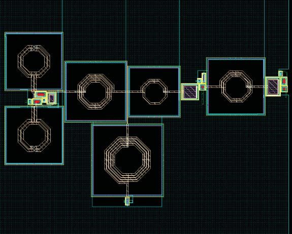
                                                                  ൅ ʹȁܿȁߙ߯ሻቋ                                     Fig. 9. Photograph of the Layout of proposed LNA

                                                                                                                     . The width of M2 transistor (288μm) is decided
                                                         ߱ ଶ                                                     considering a trade-off between gain and bandwidth.
                                               ‫ܤ‬ଶ ሺ߱ሻ ൌ ൬ ൰ ߛ ଶ ߯ ଶ ሺͳ െ ȁܿȁଶ ሻ                   (32)
                                                         ்߱                                                      Although the feedback resistor RF1= 1700Ω and RF2 =
                                                                                                                 500Ω are optimal from the simulation results due to the
                                                   At first glance at (30), shunt feedback will degrade          respectable noise performance. The value of RF1 and
                                               the minimum noise figure (NFmin), but if RF be pretty             RF2 are adjusted as 1870Ω and 411Ω, respectivelyin
                                               large, it has not very bad effect on noise figure,                order to guarantee reasonable wideband input
                                               especially it is divided on gm of transistor.                     matching.
                                                   The total noise figure (NF) can be written by                     The Rd1 and L1 are designed to achieve flat gain
                                               minimum noise figure (NFmin) and other parameters                 over the whole bandwidth and make a roll-off factor at
                                               [13] as (33):                                                     appropriate frequency. The value of L1 is designed by
                                                                                                                 two opposite requirements. It must be sizable to have
                                                                    ‫ܩ‬௡              ଶ                            large gain and it must be small so that it resonates with
                                               ܰ‫ ܨ‬ൌ ܰ‫ܨ‬௠௜௡ ൅ൌ ͳ ൅       ቂ൫ܴ௦ െ ܴ௢௣௧ ൯
                                                                    ܴ௦                            (33)           L3 and Cgs3, out-of-band, as well. Rd1 is chosen to place
                                                                                ଶ
                                                                  ൅ ൫ܺ௦ െ ܺ௢௣௧ ൯ ቃ                               the zero frequency as close as possible to the lower
                                                                                                                 edge of the band to improve the gain at lower
                                                                                                                 frequencies. An upper limit to Rd1 is set by the voltage
                                                   The total noise figure (NF) will be more than (33)            headroom. The values for the components of the load
                                               due to finite quality factor of the inductors that are used       are: Rd1 = 134Ω and L1 = 4.04nH.
                                               at the input of the transistors, the channel and gate                 The narrowband LNA is designed at 7 GHz. By the

                                                                                                                                                                                                     Journal of Iranian Association of Electrical and Electronics Engineers - Vol.14- No.4 Winter 2017
                                               noise of transistor M2 and M3 and resistor Rd1 and Rd2.           proper selection of the values for Lg, with feedback
                                               The contribution of transistor M2, M3 and M4 in noise             resistors, RF1 and RF2, the bandwidth extends to cover
                                               is much smaller than M1. For reducing the noise of the            3.1–10.6GHz. Lg for in band matching is selected as
                                               input inductor we must use inductor with high quality             595 pH.
                                               factor.                                                               The value of L2 is chosen to be 582pH for
                                                                                                                 resonating and peaking with parasitic capacitor at drain
                                               6. Circuit Design and Simulation                                  of M2 (Cd2) at the frequency of 10GHz as mentioned
                                               The layout of the finished circuit is shown in Fig. 9.            before.
                                               The layout area is 1.058 × 0.658 mm2 excluding the                    The inductor L3 at T-section makes series peaking
                                               test pads.                                                        with input capacitor from M3 transistor (Cgs3) has the
                                                   The design, simulation, post layout simulation and            value 1.96nH to smooth the gain at high frequency.
[ Downloaded from jiaeee.com on 2022-02-22 ]

                                               Trimming of the proposed CMOS UWB LNA, are                            Proper choose of inductor Lds can resonate with the
                                               based on the TSMC 0.18μm RFCMOS process. For                      parasitic capacitor at drain of M1 (Cd1) and resonates
                                               better performance at high frequencies and lower                  out of band in series with capacitor at source of M2 and
                                               parasitic, a minimum channel length of 180nm is                   drain of M1, (Cd1||Cs2) to show a broadband property. It
                                               chosen for all the transistors in the circuit.                    is chosen in this design as 582pH.
                                                   The power budget of the circuit for low power                     Second stage with 2.5mA current usage is designed
                                               designing is chosen about 10mW. So the current                    to improve the overall gain of the circuit. The width of
                                               budget is about 6mA from 1.8V voltage supply. The                 transistor M3 is chosen to 80μm. Drain resistor (Rd2) is
                                               width of M1 transistor (192μm) is optimized for noise.            chosen 200Ω to make reasonable gain for LNA. The
                                               The M1 width is sized, for 4mA current, so that the               inductor L4 has the value of 1.15nH to resonate with
                                               contributions of thermal and induced gate noise and               capacitor Cc2 and parasitic capacitor at gate of M4(Cgs4)
                                               impedance matching are balanced                                   to improve the bandwidth of the circuit.

                                                                                                                   1396 ‫ زﻣﺴﺘﺎن‬-‫ ﺷﻤﺎره ﭼﻬﺎرم‬-‫ ﺳﺎل ﭼﻬﺎردﻫﻢ‬-‫ﻣﺠﻠﻪ اﻧﺠﻤﻦ ﻣﻬﻨﺪﺳﯿﻦ ﺑﺮق و اﻟﮑﺘﺮوﻧﯿﮏ اﯾﺮان‬

                                                                                                             
The buffer must drive a 50Ω external load and is
                                                                                                                                                 used for measurements and output impedance
                                                                                                                                                 matching. The buffer is biased by means of a current                                         -10
                                                                                                                                                 source made up of one transistor. The bias current for
                                                                                                                                                 this stage is selected due to has proper output return
                                                                                                                                                                                                                                              -20

                                                                                                                                                                                                                                     S [dB]
                                                                                                                                                 loss although it reduces the power gain. The current
                                                                                                                                                 about 2.4mA is chosen for buffer stage.

                                                                                                                                                                                                                                         11
                                                                                                                                                     All design parameters are listed in Table 1. Post                                        -30       RF2=200:
                                                                                                                                                 layout simulation shows the dc current of first stage is
                                                                                                                                                                                                                                              -40       RF2=400:
                                                                                                                                                 about 3.7mA and 2.5mA for second stage. From the
                                                                                                                                                 supply voltage of 1.8V, the power consumption of the                                                   RF2=600:
                                                                                                                                                 3.1-10.6GHz LNA is 11mW, without including the                                               -50
                                                                                                                                                 output buffer stage.                                                                               2      4     6     8     10      12
                                                                                                                                                                                                                                                               freq(GHz)
                                                                                                                                                     Fig. 10 and 11 show the effect of feedback
                                                                                                                                                                                                                                       Fig. 12. Effect of variation of RF2 on S11 of the LNA
                                                                                                                                                 networks (RF1, RF2) on noise figure of the circuit. As
                                                                                                                                                 could be seen in Fig. 10 and 11 resistors feedback (RF1,
                                                                                                                                                 RF2) directly improve the noise figure at all                                                25
                                                                                                                                                 frequencies, as could be seen in (30).
                                                                                                                                                     Also Fig. 12 shows effects of RF2 on input return                                        20
                                                                                                                                                 loss. Feedback resistor (RF2) has inversely improved
                                                                                                                                                                                                                                              15
                                                                                                                                                 the S11, as shown in Fig. 12. Equation (8) shows the

                                                                                                                                                                                                                                     S [dB]
                                                                                                                                                 same results.                                                                                10

                                                                                                                                                                                                                                         21
                                                                                                                                                     Fig. 13 shows the power gain for three value of
                                                                                                                                                 inductor L1. We could see the inverse and direct                                              5        L1=2.5nH
                                                                                                                                                 relation between the value of inductor L1 and power                                                    L1=4nH
                                                                                                                                                 gain and bandwidth, respectively.                                                             0
                                                                                                                                                                                                                                                        L1=6.5nH
                                                                                                                                                                                                                                              -5
                                                                                                                                                                                                                                                           5             10              15
                                                                                                                                                           5.5
                                                                                                                                                                                                                                                               freq(GHz)
                                                                                                                                                                   RF1=1000:
                                                                                                                                                                                                                                        Fig. 13. Effect of variation of L1 on S21 of the LNA
                                                                                                                                                            5      RF1=1500:
                                                                                                                                                                   RF1=2100:                                                            Equation (4) shows the same relations. Inductor L1
                                                                                                                                                           4.5                                                                       in numerator of equation (4) has direct relation with
                                                                                                                                                  NF[dB]

                                                                                                                                                                                                                                     power gain (S21). On the other hand the inductor L1
                                                                                                                                                            4                                                                        beside inductor L3 resonates with Cgs3 to improve the
                                                                                                                                                                                                                                     bandwidth, so choosing smaller value for L1 makes
                                                                                                                                                           3.5                                                                       higher resonance frequency and it improves bandwidth.
                                               Journal of Iranian Association of Electrical and Electronics Engineers Vol14 No.4 Winter 2017

                                                                                                                                                                                                                                     So the optimum value of inductor L1 could be chosen.
                                                                                                                                                            3
                                                                                                                                                                          5         10             15                                         25
                                                                                                                                                                          freq(GHz)
                                                                                                                                                   Fig. 10. Effect of variation of RF1 on NF of the LNA                                       20

                                                                                                                                                           6.5                                                                                15
                                                                                                                                                                                                                                     S [dB]

                                                                                                                                                                   RF2=200:
                                                                                                                                                            6                                                                                 10
                                                                                                                                                                                                                                         21

                                                                                                                                                                   RF2=400:
                                                                                                                                                           5.5                                                                                          L2=1.96nH
                                                                                                                                                                   RF2=600:                                                                    5
                                                                                                                                                  NF[dB]

                                                                                                                                                            5                                                                                           L2=1.14nH
[ Downloaded from jiaeee.com on 2022-02-22 ]

                                                                                                                                                                                                                                               0
                                                                                                                                                           4.5                                                                                          L2=2.56nH
                                                                                                                                                            4                                                                                 -5
                                                                                                                                                                                                                                                           5             10              15
                                                                                                                                                           3.5                                                                                                 freq(GHz)
                                                                                                                                                                                                                                        Fig. 14. Effect of variation of L2 on S21 of the LNA
                                                                                                                                                            3
                                                                                                                                                                          5         10            15
                                                                                                                                                                         freq(GHz)                                                       Fig. 14 shows the power gain for different value of
                                                                                                                                                 Fig. 11. Effect of variation of RF2 on NF of the LNA                                inductor L2. We could see the inverse relation between
                                                                                                                                                                                                                                     the value of inductor L2 and bandwidth of the LNA.
                                                                                                                                                                                                                                     Equation (4) shows the same relation. The inductor L2
                                                                                                                                                                                                                                     resonates with Cd2 to at edge of bandwidth to improve
                                                                                                                                                                                                                                     it, so choosing smaller value for L1 makes higher

                                                                                                                                               1396 ‫ زﻣﺴﺘﺎن‬-‫ ﺷﻤﺎره ﭼﻬﺎرم‬-‫ ﺳﺎل ﭼﻬﺎردﻫﻢ‬-‫ﻣﺠﻠﻪ اﻧﺠﻤﻦ ﻣﻬﻨﺪﺳﯿﻦ ﺑﺮق و اﻟﮑﺘﺮوﻧﯿﮏ اﯾﺮان‬

                                                                                                                                                                                                                                 
resonance frequency and it could improve the
                                                                                                                         20
                                               bandwidth.
                                                        25
                                                                                                                         15
                                                        20

                                                                                                                S [dB]
                                                        15                                                               10

                                                                                                                    21
                                               S [dB]

                                                                                                                                    RF2=200:
                                                        10
                                                   21

                                                                                                                          5         RF2=400:
                                                        5     L3=512pH
                                                                                                                                    RF2=600:
                                                              L3=1.12nH
                                                        0                                                                 0
                                                              L3=260pH                                                          2        4 6      8     10      12
                                                                                                                                         freq(GHz)
                                                        -5                                                        Fig. 17. Effect of variation of RF2 on S21 of the LNA
                                                                   5               10              15
                                                                         freq(GHz)
                                                  Fig. 15. Effect of variation of L3 on S21 of the LNA              Fig. 18, 19, 20, 21, and 22 show the comparison
                                                                                                                between hand calculations and simulations of voltage
                                                   Fig. 15 shows the power gain (S21) for three value           gain (VO/VG4), (VG4/VG3), (VG3/VD2), (VD2/VIN) and NF
                                               of inductor L3. We could see the inverse relation                (noise figure). We could see in Fig. 18 the same result
                                               between the value of inductor L1 and bandwidth.                  of hand calculation and simulation result for voltage
                                               Equation (4) shows the same relation. Inductor L3                gain (VO/VG4). There are some differences between
                                               resonates with Cgs3 to improve the bandwidth, so                 hand calculation and simulation in Fig. 19 and 20 in
                                               choosing smaller value for L1 makes higher resonance             voltage gain (VG4/VG3) and (VG3/VD2). The reason for
                                               frequency and it improves the bandwidth.                         these differences is ignoring the parasitic resistance and
                                                                                                                capacitance of inductors in hand calculation, L4 for Fig.
                                                        25
                                                                                                                19 and L1, L2 and L3 for Fig. 20, respectively. Hand
                                                        20                                                      calculation and simulation result are close to each other
                                                                                                                in Fig. 21 for voltage gain (VD2/VIN). Also, there are
                                                        15                                                      some differences especially at high frequencies due to
                                               S [dB]

                                                                                                                ignoring parasitic resistance and capacitance of
                                                        10                                                      inductors Lds and Lg in hand calculation. Also
                                                   21

                                                              Rd1=135:                                          neglecting the gate-drain capacitance of M1 has some
                                                        5
                                                                                                                effects in this different result.
                                                              Rd1=88:
                                                        0                                                           The noise figure of first stage that used in hand
                                                              Rd1=177:                                          calculation has some differences with simulation result
                                                        -5                                                      due to noise of other transistors and resistors in other

                                                                                                                                                                                                      Journal of Iranian Association of Electrical and Electronics Engineers - Vol.14- No.4 Winter 2017
                                                                   5              10               15           stages that was mentioned at the end of section 5.
                                                                        freq(GHz)
                                                 Fig. 16. Effect of variation of Rd1 on S21 of the LNA
                                                                                                                          0.7
                                                   Fig. 16 shows the effect of Rd1 on power gain (S21)                                  Hand Calculation
                                               and could show the correctness of shunt peaking                           0.68           Simulation
                                               technique that is used by Rd1 and L1 at equation (4).
                                               Smaller Rd1 makes roll-off factor is happen at smaller                    0.66
                                                                                                                    G4

                                               frequency. It could be seen at Fig. 16 that the power
                                                                                                                V /V

                                               gain is falling for Rd1=88Ω, but it will rise at about 3.5
                                                                                                                    O

                                                                                                                         0.64
                                               GHz due to shunt peaking. Shunt peaking is happen for
                                               Rd1=88Ω sooner, so its rising point is happen sooner
[ Downloaded from jiaeee.com on 2022-02-22 ]

                                                                                                                         0.62
                                               compare with bigger Rd1. The rising point for bigger
                                               Rd1 is happen later, at higher frequency, so for higher
                                               Rd1 the power gain is smaller at high frequency.                           0.6
                                                                                                                                    2        4       6    8              10        12
                                                   Fig. 17 shows the effect of direct relation between                                            freq(GHz)
                                               feedback resistor and power gain. Equation (6) shows
                                               the same result. Also the bandwidth has inverse                  Fig. 18. Hand Calculation and Simulation of Voltage
                                               relation with feedback resistor as (9). So to select the                            Gain VO/VG4
                                               feedback resistor we must consider the improvement of                Fig.23 and 24 show the power gain and noise figure
                                               input return loss (as Fig.12) and power gain. On the             of CMOS UWB LNA over 3.1-10.6GHz, respectively.
                                               other hand we must mention to noise figure. So the               Noise figure (NF) is 3.6dB to 4.1dB and has ±0.25dB
                                               proper value of feedback resistor could be selected.             variations. Power gain is 15.6dB to 18.08dB was
                                                                                                                achieved over the 3.1-10.6GHz band of interest. Fig.
                                                                                                                25 shows the post layout simulation of S12 against

                                                                                                                    1396 ‫ زﻣﺴﺘﺎن‬-‫ ﺷﻤﺎره ﭼﻬﺎرم‬-‫ ﺳﺎل ﭼﻬﺎردﻫﻢ‬-‫ﻣﺠﻠﻪ اﻧﺠﻤﻦ ﻣﻬﻨﺪﺳﯿﻦ ﺑﺮق و اﻟﮑﺘﺮوﻧﯿﮏ اﯾﺮان‬

                                                                                                            
frequency of the LNA that has the value less than -39
                                                                                                                                                                                                                                                   5
                                                                                                                                                 dB in full desire band. Fig. 26 and 27 show the post                                                                           Hand Calculation
                                                                                                                                                 layout simulation of scattering parameters S11 and S22                                                                         Simulation
                                                                                                                                                 against frequency of the CMOS UWB LNA,                                                            4
                                                                                                                                                 respectively. S11 is -9.6 to -13dB and S22 is -10.8 to -

                                                                                                                                                                                                                                          NF(dB)
                                                                                                                                                 12.6dB, were achieved over the 3.1-10.6GHz band of
                                                                                                                                                 interest.                                                                                         3

                                                                                                                                                          5                                                                                        2
                                                                                                                                                                                         Hand Calculation
                                                                                                                                                         4.5                             Simulation
                                                                                                                                                                                                                                                   1
                                                                                                                                                          4                                                                                                 2       4       6    8     10        12
                                                                                                                                                                                                                                                                          freq(GHz)
                                                                                                                                                    G3

                                                                                                                                                         3.5
                                                                                                                                                  /V
                                                                                                                                                    G4

                                                                                                                                                          3                                                                              Fig. 22. Hand Calculation and Simulation of Noise
                                                                                                                                                  V

                                                                                                                                                                                                                                                              Figure
                                                                                                                                                         2.5
                                                                                                                                                          2
                                                                                                                                                         1.5                                                                                       20
                                                                                                                                                                 2        4        6     8             10        12
                                                                                                                                                                                freq(GHz)                                                          15

                                                                                                                                                                                                                                      S (dB)
                                                                                                                                                  Fig. 19. Hand Calculation and Simulation of Voltage                                              10
                                                                                                                                                                     Gain VG4/VG3
                                                                                                                                                                                                                                          21       5

                                                                                                                                                                                                                                                   0             Pre-Layout Simulation
                                                                                                                                                         2.5                                                                                                     Post-Layout Simulation
                                                                                                                                                                                                                                                   -5 0                                          1
                                                                                                                                                                                                                                                    10                                      10
                                                                                                                                                          2                                                                                                               freq(GHz)
                                                                                                                                                    G3

                                                                                                                                                         1.5
                                                                                                                                                  /V

                                                                                                                                                                                                                                                                Fig. 23. Simulated Power Gain
                                                                                                                                                    D2

                                                                                                                                                          1
                                                                                                                                                  V

                                                                                                                                                                                                                                                                 Pre-Layout Simulation
                                                                                                                                                                                                                                                10
                                                                                                                                                         0.5         Hand Calculation                                                                            Post-Layout Simulation
                                                                                                                                                                     Simulation
                                               Journal of Iranian Association of Electrical and Electronics Engineers Vol14 No.4 Winter 2017

                                                                                                                                                                                                                                                   8
                                                                                                                                                                                                                                       NF(dB)

                                                                                                                                                          0
                                                                                                                                                                 2        4        6     8             10        12
                                                                                                                                                                                freq(GHz)                                                          6

                                                                                                                                                  Fig. 20. Hand Calculation and Simulation of Voltage
                                                                                                                                                                     Gain VG3/VD2                                                                  4

                                                                                                                                                                                                                                                        0                                       1
                                                                                                                                                                                                                                                   10                                       10
                                                                                                                                                         30                                                                                                               freq(GHz)
                                                                                                                                                                     Hand Calculation
                                                                                                                                                         25          Simulation
[ Downloaded from jiaeee.com on 2022-02-22 ]

                                                                                                                                                         20                                                                                             Fig. 24. Simulated Noise Figure (NF)
                                                                                                                                                    IN

                                                                                                                                                                                                                                          Fig. 28 shows the post layout simulation group
                                                                                                                                                  /V

                                                                                                                                                         15                                                                           delay against frequency characteristics of the
                                                                                                                                                    D2

                                                                                                                                                                                                                                      CMOS UWB LNA. Simulation shows about
                                                                                                                                                  V

                                                                                                                                                         10                                                                           111±43ps of phase linearity for this circuit.
                                                                                                                                                                                                                                          The     two-tone     test     for     third-order
                                                                                                                                                          5
                                                                                                                                                                                                                                      intermodulation distortion (IP3) is shown in Fig.
                                                                                                                                                          0                                                                           29. The test is performed at 4□GHz. Tone spacing
                                                                                                                                                                2         4        6     8             10        12                   is 1MHz. The simulated IIP3 is about -9.2dBm.
                                                                                                                                                                                freq(GHz)

                                                                                                                                                  Fig. 21. Hand Calculation and Simulation of Voltage
                                                                                                                                                                     Gain VD2/VIN

                                                                                                                                               1396 ‫ زﻣﺴﺘﺎن‬-‫ ﺷﻤﺎره ﭼﻬﺎرم‬-‫ ﺳﺎل ﭼﻬﺎردﻫﻢ‬-‫ﻣﺠﻠﻪ اﻧﺠﻤﻦ ﻣﻬﻨﺪﺳﯿﻦ ﺑﺮق و اﻟﮑﺘﺮوﻧﯿﮏ اﯾﺮان‬

                                                                                                                                                                                                                                 
-40        Pre-Layout Simulation                                                            Post-Layout Simulation
                                                                   Post-Layout Simulation
                                                                                                                                    200
                                                        -50
                                               S (dB)

                                                                                                                  GD(ps)
                                                   12

                                                        -60                                                                         150

                                                        -70
                                                                                                                                    100
                                                        -80 0                                   1
                                                          10                                 10
                                                                           freq(GHz)
                                                                                                                                             0                                       1
                                                                                                                                      10                                          10
                                                                                                                                                           freq(GHz)
                                                              Fig. 25. Simulated reverse gain(dB)                                            Fig. 28. Simulated Group Delay(ps)

                                                         0
                                                                                                                                                                   IIP3 = -9.2dBm
                                                                                                                                         0
                                                         -5
                                               S (dB)

                                                                                                                  [dBm]
                                                                                                                                    -20
                                                   11

                                                        -10

                                                                                                                           out
                                                                                                                                    -40
                                                                                                                                                                 Frequency   : 4 GHz

                                                                                                                  P
                                                        -15        Pre-Layout Simulation                                                                         Tone Spacing : 10 MHz
                                                                   Post-Layout Simulation                                           -60                           Fundamental Tone
                                                              0                                 1
                                                         10                                  10                                                                   IM3 Tone
                                                                           freq(GHz)
                                                                                                                                      -40                -30         -20          -10
                                                          Fig. 26. Simulated input return loss(dB)
                                                                                                                                                               Pin [dBm]
                                                                                                                                                 Fig. 29. Simulated IIP3 at 4 GHz
                                                         -8
                                                                                                                                     -8
                                                        -10
                                                        -12
                                                                                                                                     -9
                                               S (dB)

                                                        -14
                                                                                                                  IIP3(dBm)

                                                        -16
                                                   22

                                                                                                                                                                                                             Journal of Iranian Association of Electrical and Electronics Engineers - Vol.14- No.4 Winter 2017
                                                                                                                                    -10
                                                        -18
                                                        -20        Pre-Layout Simulation                                            -11
                                                        -22        Post-Layout Simulation
                                                              0                                   1
                                                         10                                  10                                     -12
                                                                          freq(GHz)                                                    4                   6    8           10
                                                         Fig. 27. Simulated output return loss(dB)                                                  freq(GHz)
                                                                                                                                Fig. 30. Simulation IIP3 versus intermodulation
                                                                                                                                                   frequency
                                                   The IIP3 of the LNA was examined at seven
                                               different frequencies with 10 MHz frequency spacing
[ Downloaded from jiaeee.com on 2022-02-22 ]

                                               at 4, 5, 6, 7, 8, 9, and 10GHz, respectively. As in Fig.
                                               30 an average IIP3 is about -10dBm.                                                  14
                                                    Simulation results of the proposed LNAs and the                                 12
                                               prior published state-of-the-art UWB LNAs are
                                                                                                                   Quality Factor

                                               summarized in Table 1. For the comparison of different                               10
                                               topologies, we include two figures of merit (FOMs) in                                 8
                                               the table 1, FOM I, which does not include voltage
                                               supply, and FOM II, which does:                                                       6
                                                                                                                                                         590pH Symetric Inductor with
                                                                                                                                     4                   40 Pm radius and 2 turns on M6
                                                                        ܵଶଵ ‫ܹܤ‬ሺ‫ݖܪܩ‬ሻ
                                                    ‫ ܯܱܨ‬ൌ                                            (34)                           2
                                                                  ሺܰ‫ܨ‬ሺܾܽ‫̴݊݅݉ݏ‬ሻ െ ͳሻܲ஽ ሺܹ݉ሻ
                                                                                                                                                     5            10         15            20
                                                                                                                                                               freq(GHz)

                                                                                                                           1396 ‫ زﻣﺴﺘﺎن‬-‫ ﺷﻤﺎره ﭼﻬﺎرم‬-‫ ﺳﺎل ﭼﻬﺎردﻫﻢ‬-‫ﻣﺠﻠﻪ اﻧﺠﻤﻦ ﻣﻬﻨﺪﺳﯿﻦ ﺑﺮق و اﻟﮑﺘﺮوﻧﯿﮏ اﯾﺮان‬

                                                                                                             
ܵଶଵ ‫ܹܤ‬ሺ‫ݖܪܩ‬ሻ         ͳ                                                  frequency. The other inductors (L1, L2, L3 and L4) are
                                                                                                                                                 ‫ ܯܱܨ‬ൌ                                                              (35)                    chosen as standard spiral inductors. All of them have
                                                                                                                                                                ሺܰ‫ܨ‬ሺܾܽ‫̴݊݅݉ݏ‬ሻ െ ͳሻܲ஽ ሺܹ݉ሻ ܸ஽஽
                                                                                                                                                                                                                                             9μm of width on metal 6 in TSMC 0.18 μm RF CMOS
                                                                                                                                                     The table 1 shows one of the best FOM for this                                          process. Types of capacitors that are used in the circuit
                                                                                                                                                 design with very good NF and excellent power gain,                                          are MIMCAP_rf capacitor. The type of resistors and
                                                                                                                                                 although the input return loss and power consumption                                        transistors that are used in the design are listed in table
                                                                                                                                                 of the proposed circuit are in good situation. The                                          2. The post simulation results for extreme corner cases
                                                                                                                                                 values of elements that are used in the proposed circuit                                    are shown in table 3.
                                                                                                                                                 are listed in table 2. The inductors Lg and Lds are
                                                                                                                                                 symmetric spiral inductor. The simulation shows 40
                                                                                                                                                 GHz self resonance frequency for inductor Lg. The                                                Fig. 26. Quality factor of Lg (symmetrical inductor)
                                                                                                                                                 quality factor of Lg is shown as Fig. 27 against

                                                                                                                                                                                            Table. 1. Performance Compared with the Fabricated Papers*
                                                                                                                                                                                 This
                                                                                                                                                                                                    [4]            [6]             [7]          [8]       [15]      [17]      [20]        [21]      [22]
                                                                                                                                                                                Work
                                                                                                                                                    Tech(nm)                      180             180             180               180          180       90        180       180       180         180
                                                                                                                                                   BW(GHz)                      1-12.2           0.1-11        2.8-10.4           2.2-9.5     2.3-10.5   0-14.5    3-10.6     1-12    3.2-11.5     3.1-9.8
                                                                                                                                                     S21(dB)                     18.08             8.1           10.4            10.1±1.1       14±1       10      13±0.5     9.5±1   14.8±1.2     9.5±1.5
                                                                                                                                                     S11(dB)                    < -9.1
[1] FCC, Washington, DC, “First report and order,                          IEEE International Symposium on Circuits and
                                                              revision of Part 15 of the commission’s rules                         Systems (ISCAS), Paris, France, 30 May-2 June
                                                              regarding ultra wideband transmission systems,” Apr.                  2010, pp. 2470-2473.
                                                              2002, DC ET Docket 98-153.                                     [16]   Y. S. Lin and C. C. Wang and G. L. Lee and C. C.
                                                         [2] G. R. Aiello and G. D. Rogerson, “Ultra wideband                       Chen, "High-Performance Wideband Low-Noise
                                                              wireless systems,” IEEE Microwave Mag., vol. 4, no.                   Amplifier Using Enhanced π-Match Input Network,"
                                                              2, pp. 36–47, June 2003.                                              IEEE Microwave and Wireless Components Letters,
                                                         [3] K. Siwiak, “Ultra wide band radio: introducing a new                   vol. 24, no. 3, pp. 200-202, Jan. 2014.
                                                              technology,” in Proc. IEEE Vehicular Technology                [17]   K. C. He and M. T. Li and C. M. Li and J. H. Tarng,
                                                              Conf., 6-9 May 2001, pp. 1088–1093.                                   "Parallel-RC Feedback Low-Noise amplifier for
                                                         [4] P. Heydari, “Design and Analysis of a Performance-                     UWB Applications," IEEE Trans. Circuits and
                                                              Optimized CMOS UWB Distributed LNA,” IEEE J.                          Systems II: Express Briefs, vol. 57, no. 8, pp. 582-
                                                              Solid-State Circuits, vol. 42, no. 9, pp. 1892-1905,                  586, AUG. 2010.
                                                              Sept. 2007.                                                    [18]   J. H. Lee and C.C. Chen and Y.S. Lin, “0.18μm 3.1–
                                                         [5] C. W. Kim and M. S. Kang and P. T. Anh and H. T.                       10.6GHz CMOS UWB LNA with 11.4 dB gain and
                                                              Kim and S. G. Lee, “An Ultra Wideband CMOS Low                        17.4 ps group delay,” Electronics Letters, vol. 43, no.
                                                              Noise Amplifier For 3-5 GHZ UWB System,” IEEE                         24, Nov. 2007.
                                                              J. Solid-State Circuits, vol. 40, no. 2, pp. 544-547,          [19]   van deir Ziel, Noise in solid-state devices and
                                                              Feb. 2005.                                                            circuits, first edition, Hoboken, NJ: John Willey and
                                                         [6] J. F. Chang and Y. S. Lin, “0.99 mW 3–10 GHz                           Sons, 1986.
                                                              common-gate CMOS UWB LNA using T-match                         [20]   F. Liao, S. I. Liu, “A broadband noise-canceling
                                                              input network and self-body-bias technique,”                          CMOS LNA for 3.1–10.6-GHz UWB receivers,”
                                                              Electronics Letters, vol. 47, no. 11, pp. 658-659, May                IEEE J. Solid-State Circuits, vol. 42, no. 2, pp. 329–
                                                              2011.                                                                 339, Feb. 2007.
                                                         [7] Bevilacqua and A. M. Niknejad, “An ultra wideband               [21]   Y. J. Lin and S. H. Hsu and J. D. Jin and C. Y. Chan,
                                                              CMOS low-noise amplifier for 3.1–10.6-GHz                              “A 3.1–10.6-GHz ultra wideband CMOS LNA with
                                                              wireless receivers,” IEEE J. Solid-State Circuits, vol.               current-reused technique,” IEEE Microw.Wireless
                                                              39, no. 12, pp. 2259–2268, Dec. 2004.                                 Compon. Lett., vol. 17, no. 3, pp. 232–234, March
                                                         [8] J. Y. Lee and J. H. Ham and Y. S. Lee and T. Y.                        2007.
                                                              Yun, “CMOS LNA for Full-Band Ultra Wideband                    [22]   J. F. Chang and Y. S. Lin, “3.2–9.7 GHz Ultra
                                                              Systems Using a Simple Wide Input Matching                            Wideband Low Noise Amplifier with Excellent Stop-
                                                              Network,”      IET    Microwave        Antennas    and                band Rejection,” Electronics Letters, vol. 48, no. 1,
                                                              Propagation, Vol. 4, no. 12, pp. 2155–2159, Dec.                      pp. 44-45, Jan. 2012.
                                                              2010.                                                          [23] Alizadeh S, Khaleghi-Bizaki H, Okhovvat M.
                                                         [9] D. H. Shin and J. Park and C. P. Yue, “A Low-                          Improvement of TiR-UWB Communication
                                                              Power, 3–5-GHz CMOS UWB LNA Using                                     System Performance in Presence of Channel
                                                              Transformer Matching Technique,” in IEEE Int. Conf                    Estimation Error. Journal of Iranian Association
                                                              On Asian Solid-State Circuits, Jeju, S. Korea, 12-14
                                                              Nov. 2007, pp. 95-98.
                                                                                                                                    of Electrical and Electronics Engineers. 2014;
                                                         [10] Bevilacqua and C. Sandner and A. Gerosa and A.                        11 (1) :1-8

                                                                                                                                                                                                               Journal of Iranian Association of Electrical and Electronics Engineers - Vol.14- No.4 Winter 2017
                                                              Neviani, “A Fully Integrated Differential CMOS
                                                              LNA for 3–5 GHz Ultra wideband Wireless
                                                              Receivers”, IEEE Microwave and Wireless
                                                              Components Letters, vol. 16, no. 3, pp. 134-136,
                                                              March 2006.
                                                         [11] M. Khurram and S. M. R. Hasan, “A 3–5 GHz
                                                              Current-Reuse gm_Boosted CG LNA for Ultra
                                                              wideband in 130 nm CMOS,” IEEE Trans. on Very
                                                              Large Scale Integration System, vol. 20, no. 3, pp.
                                                              400-409, March 2012.
                                                         [12] Dehqan and E. Kargaran and Kh. Mafinezhad and H.
                                                              Nabovati, “An Ultra Low Voltage Ultra Low Power
                                                              CMOS UWB LNA Using Forward Body Biasing,”
          [ Downloaded from jiaeee.com on 2022-02-22 ]

                                                              in Proceedings of 55th          International Midwest
                                                              Symposium on Circuits and Systems (MWSCAS),
                                                              Mashhad, Iran, 5-8 Aug. 2012, pp. 266-269.
                                                         [13] T.H. Lee, The Design of CMOS Radio Frequency
                                                              Integrated Circuits, 2nd Edition, Cambridge, U.K.:
                                                              Cambridge Univ. Press, 2004.
                                                         [14] M. Battista and J. Gaubert and M. Egels and S.
                                                              Bourdel and H. Barthélémy, “High-Voltage-Gain
                                                              CMOS LNA For 6–8.5-GHz Receivers,” IEEE
                                                              Trans. Circuits and Systems II: Express Briefs, vol.
                                                              55, no. 8, pp. 713-717, Aug. 2008.
                                                         [15] H. M. Hsu and T. H. Lee and J. S. Huang, "Ultra
                                                              WideBand Low Noise Amplifier Using Inductive
                                                              Feedback in 90-nm CMOS," in Proceedings of 2010

                                                                                                                             1396 ‫ زﻣﺴﺘﺎن‬-‫ ﺷﻤﺎره ﭼﻬﺎرم‬-‫ ﺳﺎل ﭼﻬﺎردﻫﻢ‬-‫ﻣﺠﻠﻪ اﻧﺠﻤﻦ ﻣﻬﻨﺪﺳﯿﻦ ﺑﺮق و اﻟﮑﺘﺮوﻧﯿﮏ اﯾﺮان‬

                                                                                                                        
Powered by TCPDF (www.tcpdf.org)
You can also read