Nonlocal metasurface for circularly polarized light detection
←
→
Page content transcription
If your browser does not render page correctly, please read the page content below
134   Vol. 10, No. 1 / January 2023 / Optica                                                                      Research Article

Nonlocal metasurface for circularly polarized light
detection
Jiho Hong,1 Jorik van de Groep,1,2                            Nayeun Lee,1 Soo Jin Kim,1,3
Philippe Lalanne,4 Pieter G. Kik,1,5                                                 1,
                                                              AND Mark L. Brongersma *
1
  Geballe Laboratory for Advanced Materials, Stanford University, Stanford, California 94305, USA
2
  Current address: Van der Waals–Zeeman Institute for Experimental Physics, Institute of Physics, University of Amsterdam,
1098 XH Amsterdam, The Netherlands
3
  Current address: School of Electrical Engineering, Korea University, Seoul 02841, Republic of Korea
4
  Laboratoire Photonique, Numérique et Nanosciences (LP2N), Institut d’Optique Graduate School, University of Bordeaux, CNRS, 33400 Talence
Cedex, France
5
  CREOL, The College of Optics and Photonics, University of Central Florida, Orlando, Florida 32816, USA
*Corresponding author: brongersma@stanford.edu

Received 21 June 2022; revised 9 November 2022; accepted 11 November 2022; published 20 January 2023

      Modern-day sensing and imaging applications increasingly rely on accurate measurements of the primary physical
      quantities associated with light waves: intensity, wavelength, directionality, and polarization. These are convention-
      ally performed with a series of bulky optical elements, but recently, it has been recognized that optical resonances in
      nanostructures can be engineered to achieve selective photodetection of light waves with a specific set of predetermined
      properties. Here, we theoretically illustrate how a thin silicon layer can be patterned into a dislocated nanowire-array
      that affords detection of circularly polarized light with an efficiency that reaches the theoretical limit for circular dichro-
      ism of a planar detector in a symmetric external environment. The presence of a periodic arrangement of dislocations
      is essential in achieving such unparalleled performance as they enable selective excitation of nonlocal, guided-mode
      resonances for one handedness of light. We also experimentally demonstrate compact, high-performance chiral pho-
      todetectors created from these dislocated nanowire-arrays. This work highlights the critical role defects can play in
      enabling new nanophotonic functions and devices. © 2023 Optica Publishing Group under the terms of the Optica Open
      Access Publishing Agreement

      https://doi.org/10.1364/OPTICA.468252

1. INTRODUCTION                                                            semiconductor nanowire (NW) arrays have already been incor-
Light exhibits distinct interactions with materials that can depend        porated in multispectral detection and imaging systems [9,10].
                                                                           To gain the maximum possible information from a data stream or
on the intensity, wavelength, incident direction, and polarization
                                                                           optical scene, we need to also determine the state of polarization
state. In nanostructures, we can harness plasmonic and Mie res-
                                                                           through a measurement of the Stokes parameters [11]. Using
onances to further tailor the ways in which light interacts with
                                                                           anisotropic semiconductor NWs [12] or metallic slits [13] in the
matter. Whereas such resonant structures have primarily been
                                                                           photodetection, it is straightforward to distinguish linear states of
exploited to control the flow of light, they can also be employed
                                                                           polarization. However, the optical detection of circularly polar-
to uncover the nature of the light that is incident from an optical        ized light (CPL) is inherently more challenging. Such waves are
scene. Dense, planar arrays of nanostructures, termed meta-                comprised of two orthogonally polarized light waves for which
surfaces, have been particularly useful for this purpose as their          the electric fields are oscillating with a ±π/2 phase shift, and this
diffraction behavior is very sensitively dependent on the properties       relative phase information is lost in the photodetection process. As
of light waves. For example, they have successfully been used to           a result, CPL detection typically involves the use of a quarter-wave
perform spectropolarimetry by decomposing plane waves into a               plate and linear polarizer on top of a (non-chiral) photodetector.
set of separated beams that each carry information on the incident         In fact, many invertebrates such as mantis shrimp, cuttlefish, bees,
angle, spectral content, and polarization state [1–8]. However,            and crickets have developed such compound elements to create
such metasurfaces need to be used in conjunction with a separate           CPL-sensitive detection systems for communication and visual
image sensor to create a complete spectro-polarimetric system. To          contrast enhancement [14]. It is, however, well worth exploring
allow further device integration, it is critical to explore whether        new ways to measure the properties of CPL, given its increasingly
the spectral/polarization decomposition and the photodetection             prominent role in many applications, including quantum optics
processes can be combined in a single metasurface. Recently,               [15] and communication [16], drug design and development

2334-2536/23/010134-08 Journal © 2023 Optica Publishing Group
                                                       Corrected 26 January 2023
Research Article                                                                                                             Vol. 10, No. 1 / January 2023 / Optica   135

[17], remote sensing [18] and spectropolarimetry [19], imaging                                extended, high optical, quality-factor modes and momentum-
[20], valley optoelectronics [21], and topological photonics [22].                            dependent transfer functions. In our case, the nonlocal resonance
Recent pioneering approaches include detectors that employ                                    selectively enables substantial optical absorption and photocarrier
chiral organic molecules and semiconductors [23–25] and chiral                                generation in the semiconductor material for the circular polariza-
plasmonic structures [26,27]. Plasmonic structures can show                                   tion (CP) of interest. The polarization can therefore be determined
particularly high circular dichroism (CD), i.e., differential absorp-                         through a measurement of the photocurrent upon application of
tion for left- and right-handed CPL [27–30], but metals tend to                               a small bias voltage to the electrodes. A scanning electron micro-
make poor photodetectors that can only rely on inefficient hot                                graph (SEM) of an array fabricated by electron beam lithography is
electron emission. To boost the responsivity, it is highly desir-                             shown in Fig. 1(b).
able to explore whether chiral detectors can be made from high                                    Before we provide a detailed mechanistic picture of the metasur-
electrical-performance, inorganic, achiral semiconductors. Here,                              face operation, we evaluate the fundamental performance limit for
we show that a dislocated silicon nanowire (Si NW) metasurface                                this type of device using coupled-mode theory [38,39]. Because of
can effectively detect and distinguish left- and right-handed CPL                             its two-dimensional nature, the detector can be treated as a single-
without the need of external filters or waveplates.                                           mode optical resonator in a symmetric external environment.
                                                                                              The incident CPL can follow a direct transmission pathway and
                                                                                              a resonant pathway through the nanopatterned semiconductor
2. RESULTS                                                                                    layer [Fig. 1(c)]. When the light follows the resonant pathway and
Figure 1(a) shows a conceptual schematic of our proposed CD                                   the guided resonance is excited, it leads to significantly increased
photodetector. It features a dense array of custom-designed Si                                energy storage and light absorption. To maximize the CD, we
NWs on a transparent substrate. The unique shape of the NWs                                   would ideally construct a situation where the incident light can
with a periodic array of kinks is engineered to facilitate excitation                         only excite the resonance when its polarization matches the desired
of a nonlocal guided-mode resonance by normally incident CPL                                  handedness. In our example, this will be right-handed circular
with one selected handedness while transmitting light waves of the                            polarization (RCP). To achieve the strongest possible light absorp-
opposite handedness. Recently, there has been an increased interest                           tion, a fraction of the in-coupled light needs to couple back out into
in flat optical elements with nonlocal optical resonances [31–37]                             free space in order to effectively cancel out the directly transmitted
as they enable high-performance imaging, sensing, and modula-                                 light through destructive interference. The reciprocal nature of
tion functions. These flat optical elements display more spatially                            this device enforces that on resonance, the out-coupled light from

                               (a)                                                        (c)              RCP                             LCP
                                                                                                                          R=0.25

                           z
                                                                   0
                                    y
                                                                       A
                                                                            1                                    A=0.5
                                x

                                                                                Iph
                                                                                             half-wave
                                                                                               plate
                                        Si
                                                                                                                  λ/2

                                                                       Al
                                                                                                                                           T=1
                                                            Sapphire                                             T=0.25

                               (b)                                                       (d)
                                                                                                    0.5                                    |Hy/H0|
                                                                                                                        RCP        RCP         40
                                                                                                    0.4
                                                                                      Absorptance

                                                                                                    0.3                            LCP

                                                                                                    0.2
                                                                                                                                                 0

                                                                                                    0.1
                                                                                                                          LCP
                                                                                                     0
                                                                                                     750                800                          850
                                                                                                                   Wavelength (nm)

Fig. 1. Dislocated high-index semiconductor metasurfaces for CD. (a) The schematic of a CD photodetector using dislocated high-index semiconduc-
tor metasurfaces. A dislocated Si NW metasurface displays resonant absorption for a CP of interest (RCP, red) while transmitting the other (LCP, blue),
allowing an electrical read-out of an incident CP. (b) The SEM of fabricated Si nanostructures. A unit cell of the periodic structures is outlined by the white
box. Scale bar, 500 nm. (c) The illustration of an optically resonant nanopatterned semiconductor layer in free space interacting with incident RCP (left)
and LCP (right) at critical coupling. (d) The simulated optical absorption spectra of a dislocated Si NW metasurface suspended in free space for RCP (red)
and LCP (blue). The Si metasurface is designed to present resonant absorption for the RCP at λ = 800 nm. The theoretical limit of absorptance is indicated
by the black dashed line. Inset: Normalized magnetic field distributions (λ = 800 nm) in the median plane of two adjacent unit cells for the RCP (top) and
the LCP (bottom). Scale bar, 200 nm.
Research Article                                                                                Vol. 10, No. 1 / January 2023 / Optica   136

the resonator changes its handedness in the transmission direction       the architecture of a metamaterial crystal is typically linked to its
(Supplement 1, Note 1). As a result, we see that left-handed circular    optical properties, recent work has also demonstrated the powerful
polarization (LCP) emerges given an RCP incident beam. In order          benefits of controllably introducing defects and disorder to achieve
for the directly transmitted light to interfere destructively with       new properties not seen in perfect crystals [48–53]. In engineered
the out-coupled light, its polarization should thus also have the        metamaterials, the ability to continuously tune the geometry and
opposite handedness and incur a π phase delay with respect to the        size of defects can afford profound new insights into the evolution
resonant pathway. In other words, it is essential that the slab serves   of certain physical properties with varying defect parameters. In
as a half-wave plate for the direct transmission channel. This is a      turn, such fine-tuning allows one to reach fundamental perform-
key insight of our analysis as it provides valuable intuition about      ance limits. Here, we follow this approach for our dislocated NW
possible device designs. Analogous to optical absorption in an           metasurfaces.
ultrathin and freely suspended metallic film [40], the theoretical           We employ a scattered field formalism (Supplement 1, Note 2)
limit for the absorptance of the RCP light is 0.5 at critical coupling   to show how the introduction of dislocations can have a dramatic
when both the total transmittance and reflectance are 0.25.              impact on the optical properties of the metasurface. Our analysis
    Leveraging the insights derived from coupled-mode theory,            indicates that the dislocations can serve as secondary localized
we aim to identify a nanostructure design for the suspended sili-        sources of scattered fields that control the coupling of free-space
con (Si) film that can both serve as a half-wave plate for the direct    light waves to quasi-guided, nonlocal modes supported by the
transmission pathway and only exhibit an optical resonance for the       NW array. At the elementary level, this point is illustrated in
RCP light. Figure 1(d) shows the optical absorption behavior of          Fig. 2(a) for a single, dislocated, 50-nm-thick Si NW illuminated
our successfully optimized design, as obtained by finite-element         by transverse-magnetic (TM) incident light, where the electric
simulations. As desired, the spectrum for LCP illumination shows         field is directed along the NW axis. The incident electric field
a low and relatively constant absorptance across the wavelength          drives an oscillating displacement current D (dark blue arrows)
range of interest. This results from the non-resonant absorption         along the semi-infinite NW (x -direction). The introduction of
channel where light is directly transmitted through the film with        a kink in the NW results in discontinuities in the permittivity
little dissipation in the Si. On the other hand, the absorption spec-    and accumulation of positive and negative surface charges at the
trum for the RCP light displays a spectrally narrow resonance with       newly created corners (Supplement 1, Fig. S2). The surface charge
a high optical quality factor, Q = 180. The metasurface achieves         distributions for this very thin NW form a localized electric dipole
critical coupling, and the absorptance on resonance is just above        that is oriented perpendicular to the incident electric field. This
the theoretically predicted limit. The slightly larger absorption        dipole orientation allows effective radiation into the guided modes
results from the small amount of non-resonant absorption in              of both semi-infinite NWs.
the finite-thickness film. The magnetic field distributions in the           Next, we aim to create dislocations capable of selectively cou-
nanostructured layer on and off resonance are shown as insets. For       pling the CPL of one desired handedness. We show a conceptually
RCP, the high-Q resonance gives rise to a strong field enhancement       intuitive strategy that builds on the observation that CPL is com-
inside the NWs. This enables significant optical absorption in the       posed of two orthogonally polarized light waves for which the
Si despite its weak material absorption. In the following, we will       electric fields are oscillating with a ±π/2 phase shift. If the dis-
discuss the intuitive design for the NWs and the physics behind the      locations can enable the coupling of both the incident TM and
operation of our CPL detector.                                           the orthogonal, i.e., transverse-electric (TE) polarizations to the
    In the design of our metasurface-based photodetector, we aim         same guided mode of the NW, then we can control the excitation
to use high electrical-performance semiconductors and avoid the          efficiency of the guided-mode resonance by manipulating their
use of complex and hard-to-integrate three-dimensional chiral            optical interference. Constructive/destructive interference and a
systems, such as arrays of helices [28] and twisted optical metama-      concomitant high/low excitation efficiency can result depending
terials [29,41,42]. Fortuitously, it has been shown that a strong        on the relative phase of the two excited waves. Dislocations in
CD can also be obtained in planar chiral metasurfaces [27,43,44],        larger NW sizes can accomplish this as they can produce a variety
i.e., metasurfaces that are distinguishable from their mirror images     of higher-order multipolar sources of scattered fields. Through
(enantiomers) with respect to a line in the plane of the structure.      the scattered field formalism, we can identify the nature of the
We start the design of our planar chiral metasurface by considering      multipolar sources as it naturally connects the oscillating charge
the optical properties of a dense, subwavelength array of straight Si    distributions at the dislocations to the excited resonances in the
NWs. Such anisotropic, non-diffractive structures exhibit artificial     NWs [54]. For example, the illumination of a dislocated 180-
birefringence and can be engineered to serve as a half-wave plate        nm-thick NW with 800 nm light gives rise to the formation of an
[45], satisfying our first design requirement. We can also easily        electric quadrupole for TM polarization [Fig. 2(b)] and a magnetic
turn NWs into photodetectors by electrically contacting both             dipole for TE polarization [Fig. 2(c)]. The electric quadrupole,
ends, and they have already been implemented to selectively detect       induced for TM polarization, can be considered as a set of electric
light of specific wavelengths, linear polarizations, and incident        dipoles oriented anti-parallel in the horizontal and vertical direc-
angles [12,46]. Without modification, linear NW-arrays exhibit           tions [as illustrated in Fig. 2(b)]. As they are placed off the NW
identical optical responses for both CPs. However, the introduc-         axes on both sides, these anti-parallel pairs can radiate into the
tion of a series of localized displacements in the NWs [see Fig. 1(a,    semi-infinite NWs with the same parity as a magnetic dipole. For
b)] renders the metasurface planar chiral and produces distinct          TE polarization, similarly to the electric dipole induced in a thin
optical responses for the RCP and the LCP light. These displace-         Si NW [Fig. 2(a)], the magnetic dipole is oriented perpendicular
ments are reminiscent of the atomic displacements that occur             to the incident magnetic field. This polarization conversion is a
near a dislocation core in a real crystal [47], and for this reason,     key ingredient for our strategy as it allows effective coupling into
we term the structure a dislocated NW metasurface. Whereas               the same guided mode for the two orthogonal polarizations of the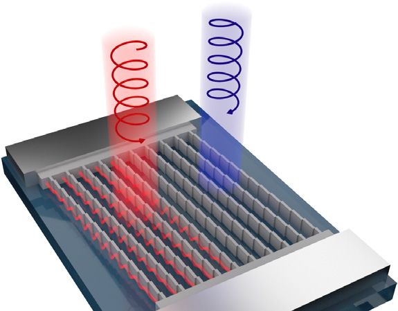
Research Article                                                                                                Vol. 10, No. 1 / January 2023 / Optica      137

           a                                                                                                        TM     E

                                 TM                                                                                k       H
                                        E
                                                                  D
                                 k      H

                                                                                                                                               p

                                                          z                                                                       e
                                                                                                                            Re(σ s) (a.u.)
                                                  y                   x                                                                                x
                                                                                                                           -1    0    1
                                                                                                                                                   y       z

           b                                TM    E                                c                                TE     H
                                                                                                               E
                                            k      H                                                                   k

                                                                          Qe                                                                   m

                                                              e                                      E                           m
                                                      Re(σ s) (a.u.)                                                        Re(J s,y) (a.u.)
                                                                                                     H
                           D                       -1      0          1                                                    -1    0    1

Fig. 2. Light scattering from a dislocation in a single Si NW. (a) The schematic of a thin Si NW (left) and a dislocated Si NW (right, δ = 40 nm) for
TM polarization (h = 50 nm, w = 100 nm). The simulated surface electric charge density distribution (λ = 800 nm) is overlaid on the interface between
two semi-infinite NWs (right), serving as a localized electric dipole p that radiates back into the guided modes of each semi-infinite NW. (b) and (c) The
schematic of a dislocated Si NW with a larger height (h = 180 nm, w = 100 nm, δ = 40 nm) for (b) TM and (c) TE polarizations. The simulated surface
electric charge density distribution [(b), λ = 800 nm] and surface magnetic current density distribution [(c), λ = 800 nm] are overlaid on the interface
between two semi-infinite NWs, serving as a localized electric quadrupole Q e (b) (represented by a set of electric dipoles oriented anti-parallel in the hori-
zontal and vertical directions) and a localized magnetic dipole m (c), respectively. In (a)–(c), the phases of the incident fields are chosen differently to clarify
induced different multipolar sources of the scattered field.

incident light. As a result, the excitation for one handedness can                       Next, we introduce a single dislocation in the NWs placed in
be selectively enhanced through constructive interference, which                     an array and show how its geometrical properties can be designed
occurs when these different excitation processes compensate for the                  to effectively couple both TM- and TE-polarized light to the same
π/2 phase shift between the TM- and TE-polarized components.                         fundamental guided Bloch mode of the NW array [see Fig. 4(b) for
Due to the anisotropic shape of NWs, this can simply be achieved                     the dispersion relation and the field distributions of the fundamen-
by placing the optical resonances for these two polarizations at                     tal mode]. Figure 3(c) shows how the amplitudes and relative phase
different spectral locations.                                                        of the excited mode vary with the size of the dislocation for TM and
   With all of the relevant design concepts in place, we are now                     TE polarizations (Supplement 1, Note 3). The amplitudes display
in a position to use optical simulations to identify an optimal                      a notable dependence on δ for both polarizations. Because each
design for operation at the preselected wavelength of 800 nm,                        polarization induces distinct localized sources at the dislocation
as schematically shown in Fig. 3(a). We start by considering                         (Fig. 2), it is not surprising that the coupling cross sections for TM
a Si NW array without dislocations, i.e., with a displacement                        and TE polarizations vary differently with δ. This allows us to find
δ = 0 nm, to optimize the direct transmission pathway for the                        a certain value of δ (6 = 0), where the amplitudes of the excited
light. Using the finite-element technique, we identify NW peri-                      mode are identical for both polarizations. On the other hand, the
ods 3 y , heights h, and widths w, for which the array serves as                     relative phase of the excited waves is independent of δ and equal
a half-wave plate, requiring a π phase shift between transmit-                       to −π/2 regardless of δ. This phase difference is strongly linked
ted TM- and TE-polarized light. Whereas multiple geometries                          to the direct transmission properties of a Si NW array. From the
meet this basic requirement, we identify that a subwavelength                        coupled-mode theory, it follows that the phase difference must
period 3 y = 500 nm offers easy-to-fabricate solutions and a high                    be ±π/2 when a Si NW array serves as a half-wave plate in the
transmittance. Figure 3(b) shows the transmittance for differ-                       direct transmission (Supplement 1, Note 4). In the scattered field
ent NW heights and widths together with a shaded region that                         description, this phase difference results from the relative phase of
highlights the set of solutions for which the phase shift between                    the total fields inside the semi-infinite NWs for the TM and TE
TM- and TE-polarized light is close to the desired value of π.                       polarizations. To produce a π phase shift in the direct transmission,
Among these solutions, we choose the dimensions for the NWs as                       the Si NW array operates near a Fabry–Perot resonance for TM
h = 185 nm and w = 95 nm [white dot in Fig. 3(b)], and we use                        polarization and off-resonance for TE polarization (Supplement
these throughout this work for the Si NW arrays suspended in free                    1, Fig. S4). This gives rise to the π/2 phase difference of the total
space [Figs. 3(c), 3(d) and 4].                                                      fields inside the NWs for TM and TE polarizations, which is
Research Article Vol. 10, No. 1 / January 2023 / Optica 138
Average transmittance ( =0)
TM TE
E E H 250 1 30 0
(a) (b) (c)
Coupling cross section (nm)
k H k 0.8
Phase difference (rad)
200
20
150 0.6
h (nm)
y
- /2
100 0.4
10
(c) TE
w 0.2
z (b)
50
TM
y x
h 0 0 -
50 100 150 200 250 20 30 40
w (nm) (nm)
(d) Einc Re(Hsca,y/H0) Hsca,y
Im
TM 1 Re
Im
TE Re
eff
/4
y
0
z x
Im Im
RCP Re + Re
Im Im
-1
LCP Re + Re
Fig. 3. Polarization-controlled excitation of guided waves at single dislocation. (a) The schematic of a single dislocation introduced into a Si NW array
(3 y = 500 nm). For LPs, excited guided waves are examined at a position away from the dislocation (indicated by the black dashed box). (b) The simulated
average transmittance (λ = 800 nm) of a non-dislocated Si NW array (δ = 0) for LP illumination. The highlighted band indicates the set of the geometries,
which provide the desired π phase shift (in a range of ±0.05π) between TM- and TE-polarized light in transmission. The white dot indicates the dimen-
sions for the NWs used in (c) (h = 185 nm, w = 95 nm). (c) The simulated coupling cross sections (solid) and phase difference (dashed) of the fundamen-
tal guided mode (λ = 800 nm) excited for TM and TE polarizations as a function of δ (6 = 0). The coupling cross sections for LPs are identical around δ =
30 nm. (d) The normalized scattered magnetic field distributions and their phasor representations (λ = 800 nm) for different incident polarizations. The
phasor representations are broken down into contributions from TM- (magenta) and TE- (cyan) polarized incident fields to illustrate interference between
them. Scale bar, 200 nm.
directly translated to the scattered fields by their induced sources at design and the CP excitation leads to constructive (or destructive)
the dislocation. interference between the excited waves by TM and TE polariza-
Figure 3(d) shows the scattered field distributions of the sin- tions [Fig. 3(d)]. Therefore, only incident light for the RCP can
gle dislocation for different incident polarizations. From the excite the fundamental guided mode in the dislocated Si NW array.
scattered fields for TM and TE polarizations, we can see that the The phasor representation for the scattered fields is also shown for
fundamental guided mode is launched from the dislocation and each incident polarization.
propagates along the semi-infinite Si NW array in both direc- A single, subwavelength dislocation only couples a small
tions. As the dislocation size (δ = 30 nm) is chosen to give rise to fraction of the incident light at one very specific location. By peri-
the same excitation amplitude for linear polarizations (LPs), the odically arranging dislocations in the Si NW array along the NW
excited guided waves for TM and TE polarizations display the length, we can resonantly enhance the polarization-controlled
same magnitude but with a quarter effective wavelength delay excitation of the quasi-guided wave [Fig. 4(a)]. For an incident
between them dictated by the nanoscale geometry. When RCP (or RCP plane wave, the fundamental mode is excited at each dis-
LCP) is illuminated, both TM and TE polarization components location and quasi-guided waves are launched along the Si NW
contribute simultaneously to the excitation of the guided wave. array [see Fig. 3(c)]. When the period 3x of the dislocations is
Note that the incident CP provides additional +π/2 (or −π/2) chosen to be close to the effective wavelength of the fundamental
phase delay between the excitation by the two LP components. mode, the quasi-guided waves excited at each dislocation interfere
Combined, the phase delay resulting from the nanostructure constructively with each other to build up a collective resonance
Research Article                                                                                                                 Vol. 10, No. 1 / January 2023 / Optica   139

                                                                                                           600
                               a                 RCP                                                                 b

                                                                                                                            air
                                                                           LCP
                                                                                                           500                            TM 00

                                                                                         Frequency (THz)
                                                                                                                                                    TE 00           Si
                                                                                                           400

                                                                                                                                                  |Hy|            |Ez|
                                                                                                           300                                       1               1

                                                                     Λx
                                       z                                                                   200                                      0                0
                                   y         x
                                                                                                                 0              2             4                          6
                                                                                                                           Propagation constant (μm-1)

                                                                                                                           RCP                           LCP
                                                                                                             1
                         0.5
                               c                 RCP                       |Hy/H0|                                   d                       e
                                                               RCP             40                     0.75
                         0.4                                                                                                       20
                                                                                                                              1
           Absorptance

                                                                                         T/R/A
                         0.3
                                                               LCP                                         0.5

                         0.2                                                                                                  0                     T       R       A
                                                                                                                                   800
                                                                               0                      0.25
                         0.1               CD
                                                    LCP
                          0                                                                                  0
                          380          400       420     440         460           480                               750   800     850      750 800              850
                                                   Λx (nm)                                                                        Wavelength (nm)
Fig. 4. Resonantly enhanced absorption using guided-mode resonance. (a) The schematic of periodic dislocations introduced into the Si NW array
designed in Fig. 3. At each dislocation, the fundamental guided mode is excited for the RCP [Fig. 3(d)], and quasi-guided waves are launched along the
Si NW array. (b) The simulated dispersion relations for the first two guided Bloch modes of the non-dislocated Si NW array. The white dot indicates the
fundamental guided mode at λ = 800 nm. The black lines indicate the light lines in the air and the Si, respectively. Inset: Magnetic (left) and electric (right)
field distributions of the guided mode at the point indicated in the dispersion relation. Scale bar, 100 nm. (c) The simulated absorptance (λ = 800 nm) for
RCP (red) and LCP (blue) and corresponding CD (black) as a function of 3x . Inset: Normalized magnetic field distributions for the RCP (top) and the LCP
(bottom) at the absorption peak (3x = 430 nm). Scale bar, 200 nm. (d) and (e) Simulated transmittance (T, solid), reflectance (R, dashed), and absorptance
(A, grey) spectra (3x = 430 nm) for the RCP [red, (d)] and the LCP [blue, (e)]. Inset: Optical spectra for the RCP near the resonance wavelength (over the
shaded range). The black dashed lines indicate 0.25 and 0.5, respectively.

(guided-mode resonance). The Q of such a resonance is limited                                      of the CD is slightly smaller than the theoretical limit due to the
by the material absorption and the amount of scattered light into                                  non-resonant absorption. This procedure led us to choose the NW
free-space radiation at the dislocations. Given the weak material                                  dimensions above (h = 185 nm, w = 95 nm).
loss and small size of the dislocations, we can achieve a high-Q                                       Figures 4(d) and 4(e) show the simulated transmission and
resonance [55–58]. The period needed to achieve a guided-mode                                      reflection spectra of the periodically dislocated Si NW array for
resonance at the chosen operation wavelength of 800 nm can be                                      RCP and LCP, respectively. The spectra for the LCP display a high
approximately obtained from the simulated dispersion relation for                                  transmittance and low absorptance over a broad spectral range,
the guided mode [Fig. 4(b)]. The resonance strongly enhances the                                   with a slow overall variation that results from a spectrally broad
RCP light absorption, while the incident light for LCP presents                                    Fabry–Perot resonance supported by the nanostructured film/NW
only weak, non-resonant absorption [Fig. 4(c)]. To maximize the                                    array. On the other hand, the spectra for the RCP exhibit not only
resonant absorption from the guided-mode resonance, we can                                         the broad Fabry–Perot resonance but also the spectrally narrow
carefully adjust the radiative and absorption decay rates of the                                   guided-mode resonance, which leads to strong resonant absorp-
resonance to balance them. This is possible by exploring different                                 tion. As these resonances are spectrally overlapped, the scattered
combinations of NW heights and widths in the highlighted region                                    light through the guided-mode resonance interferes with the trans-
in Fig. 3(b). For each combination of h and w, the other dimen-                                    mitted light through the Fabry–Perot resonance, which gives rise to
sions, δ and 3x , are determined accordingly as described above                                    a large and spectrally narrow variation in both the transmission and
(3 y is fixed). This procedure enables us to achieve critical coupling                             reflection spectra for RCP. On the guided-mode resonance, both
for the dislocated Si NW array and a CD close to the theoretical                                   the total transmittance and reflectance become ∼0.25 and allow us
limit of 0.5 (Supplement 1, Note 5). Note that the maximum value                                   to achieve an absorptance of ∼0.5.
Research Article Vol. 10, No. 1 / January 2023 / Optica 140
3
a b c
∆EQE (×10-4)
0.2
0.3 1
CD
2
Absorptance
0
EQE (×10-4)
Si 0.2 RCP RCP
0
750 800 850 750 800 850
Sapphire
0.1 1
LCP
Al LCP
0
0
750 800 850 750 800 850
Wavelength (nm) Wavelength (nm)
Fig. 5. Experimental demonstration of a CD photodetector. (a) The reflected optical micrograph of the fabricated CD photodetector under white-light
illumination. Scale bar, 25 µm. Inset: SEM of a unit cell of the fabricated Si nanostructures. Scale bar, 50 nm. (b) The measured optical absorption spectra
for the RCP (red) and the LCP (blue). Inset: Measured CD spectrum. The grayed-out areas in optical spectra indicate the spectral range in which first-order
diffraction channels open up in the transparent substrate. (c) The measured EQE spectra for the RCP (red) and the LCP (blue). Inset: Measured differential
EQE spectrum.
To experimentally demonstrate a CD photodetector, we fabri- maximum of CD in a symmetric external environment. We exper-
cate a periodically dislocated Si NW array on a transparent sapphire imentally implement the metasurface in a CD photodetector and
substrate [Fig. 5(a)]. We slightly redesign the geometry of the dis- verify the key physics behind its operation using optical absorption
located Si NW array (3x = 370 nm, 3 y = 430 nm, h = 320 nm, and photocurrent measurements. These dislocated nanostructures
w = 65 nm, and δ = 35 nm) to take into account the presence of can be employed in a range of applications for polarimetric sensing
the substrate (Supplement 1, Fig. S6). For photocurrent extraction, and imaging where dense integration is required.
we fabricate aluminum ohmic contacts at the ends of the dislo-
Funding. Air Force Office of Scientific Research (FA9550-18-1-0323,
cated Si NW array (43 × 37 µm2 ). Next, we first characterize the FA9550-21-1-0312); U.S. Department of Energy (DE-FG07-ER46426);
optical absorption of the fabricated CD photodetector [Fig. 5(b)]. National Science Foundation (ECCS-2026822).
From transmission and reflection measurements, we calculate the
absorptance by subtracting the transmittance and reflectance from Acknowledgment. We would like to acknowledge support from an
individual investigator from the Airforce, a Multidisciplinary University
unity. In the experimental absorption spectra, the dislocated Si Research Initiative from the Air Force Office of Scientific Research, and from
NW array exhibits a high-Q optical resonance for the RCP light the Department of Energy. Part of this work was performed at the Stanford
only. The sensitivity of the resonance to the handedness of the light Nano Shared Facilities (SNSF) and the Stanford Nanofabrication Facility (SNF),
results in a significant CD on resonance, corroborating the selec- supported by the National Science Foundation.
tive modal excitation described above. The grayed-out areas in the
Disclosures. The authors declare no conflicts of interest.
optical spectra correspond to the spectral range in which first-order
diffraction channels open up in the transparent sapphire substrate. Data availability. The data that support the plots within this paper and other
As the diffracted light is not captured in the measurements, the findings of this study are available from the corresponding author upon reasonable
request.
calculated absorptance is higher than the actual amount in this
spectral range. With an applied external bias, we also characterize Supplemental document. See Supplement 1 for supporting content.
the photocurrent response of the CD photodetector [Fig. 5(c)].
For both RCP and LCP, the measured external quantum effi-
ciency (EQE) spectra are consistent with the experimental optical REFERENCES
absorption spectra. A resonantly enhanced EQE for RCP light over 1. Z. Bomzon, G. Biener, V. Kleiner, and E. Hasman, “Spatial Fourier-
LCP light is observed, and we can use this to directly distinguish transform polarimetry using space-variant subwavelength metal-stripe
polarizers,” Opt. Lett. 26, 1711–1713 (2001).
between these polarization states. Note that the spectral broaden- 2. A. Pors, M. G. Nielsen, and S. I. Bozhevolnyi, “Plasmonic metagrat-
ing of the EQE spectra, as compared to the absorption spectra, can ings for simultaneous determination of Stokes parameters,” Optica 2,
be attributed to a spatially dependent charge collection efficiency 716–723 (2015).
(Supplement 1, Note 6). We also experimentally demonstrate a 3. J. P. Balthasar Mueller, K. Leosson, and F. Capasso, “Ultracompact
metasurface in-line polarimeter,” Optica 3, 42–47 (2016).
CD photodetector with resonant absorption and EQE for LCP by
4. A. Basiri, X. Chen, J. Bai, P. Amrollahi, J. Carpenter, Z. Holman, C. Wang,
simply reversing the direction of the displacements for each of the and Y. Yao, “Nature-inspired chiral metasurfaces for circular polarization
dislocations (Supplement 1, Fig. S7). detection and full-Stokes polarimetric measurements,” Light Sci. Appl.
8, 78 (2019).
5. S. Yokogawa, S. P. Burgos, and H. A. Atwater, “Plasmonic color filters for
3. CONCLUSION CMOS image sensor applications,” Nano Lett. 12, 4349–4354 (2012).
6. M. L. Brongersma, “Plasmonic photodetectors, photovoltaics, and hot-
In conclusion, we demonstrate the use of a nonlocal semiconduc- electron devices,” Proc. IEEE 104, 2349–2361 (2016).
tor metasurface to build an integrated photodetector for circularly 7. A. McClung, S. Samudrala, M. Torfeh, M. Mansouree, and A. Arbabi,
polarized light. Using a dislocation as a building block, we are able “Snapshot spectral imaging with parallel metasystems,” Sci. Adv. 6,
eabc7646 (2020).
to systematically design a Si metasurface that displays a guided- 8. M. I. Benetou, B. C. Thomsen, P. Bayvel, W. Dickson, and A. V. Zayats,
mode resonance only for a circular polarization of interest. The “Four-level polarization discriminator based on a surface plasmon
engineering of the resonance allows us to reach the theoretical polaritonic crystal,” Appl. Phys. Lett. 98, 111109 (2011).Research Article Vol. 10, No. 1 / January 2023 / Optica 141
9. H. Park, Y. Dan, K. Seo, Y. J. Yu, P. K. Duane, M. Wober, and K. B. Crozier, 34. A. C. Overvig, S. C. Malek, and N. Yu, “Multifunctional nonlocal metasur-
“Filter-free image sensor pixels comprising silicon nanowires with selec- faces,” Phys. Rev. Lett. 125, 017402 (2020).
tive color absorption,” Nano Lett. 14, 1804–1809 (2014). 35. M. Lawrence, D. R. Barton, III, J. Dixon, J.-H. Song, J. van de Groep, M.
10. Q. Li, J. van de Groep, Y. Wang, P. G. Kik, and M. L. Brongersma, L. Brongersma, and J. A. Dionne, “High quality factor phase gradient
“Transparent multispectral photodetectors mimicking the human visual metasurfaces,” Nat. Nanotechnol. 15, 956–961 (2020).
system,” Nat. Commun. 10, 4982 (2019). 36. S. J. Kim and M. L. Brongersma, “Active flat optics using a guided mode
11. C. F. Bohren and D. R. Huffman, Absorption and Scattering of Light by resonance,” Opt. Lett. 42, 5–8 (2017).
Small Particles (Wiley, 1983). 37. S. C. Malek, A. C. Overvig, S. Shrestha, and N. Yu, “Active nonlocal
12. L. Cao, J. S. White, J.-S. Park, J. A. Schuller, B. M. Clemens, and M. L. metasurfaces,” Nanophotonics 10, 655–665 (2020).
Brongersma, “Engineering light absorption in semiconductor nanowire 38. H. A. Haus, Waves and Fields in Optoelectronics (Prentice-Hall, 1984).
devices,” Nat. Mater. 8, 643–647 (2009). 39. S. Fan, W. Suh, and J. D. Joannopoulos, “Temporal coupled-mode the-
13. F. Afshinmanesh, J. S. White, W. Cai, and M. L. Brongersma, ory for the Fano resonance in optical resonators,” J. Opt. Soc. Am. A 20,
“Measurement of the polarization state of light using an integrated 569–572 (2003).
plasmonic polarimeter,” Nanophotonics 1, 125–129 (2012). 40. W. Woltersdorff, “Über die optischen Konstanten dünner
14. T.-H. Chiou, S. Kleinlogel, T. Cronin, R. Caldwell, B. Loeffler, A. Siddiqi, Metallschichten im langwelligen Ultrarot,” Zeitschrift für Phys. 91,
A. Goldizen, and J. Marshall, “Circular polarization vision in a stomato- 230–252 (1934).
pod crustacean,” Curr. Biol. 18, 429–434 (2008). 41. X. Yin, T. Steinle, L. Huang, T. Taubner, M. Wuttig, T. Zentgraf, and
15. J. F. Sherson, H. Krauter, R. K. Olsson, B. Julsgaard, K. Hammerer, H. Giessen, “Beam switching and bifocal zoom lensing using active
I. Cirac, and E. S. Polzik, “Quantum teleportation between light and plasmonic metasurfaces,” Light Sci. Appl. 6, e17016 (2017).
matter,” Nature 443, 557–560 (2006). 42. X. Yin, M. Schäferling, B. Metzger, and H. Giessen, “Interpreting chiral
16. R. Farshchi, M. Ramsteiner, J. Herfort, A. Tahraoui, and H. T. Grahn, nanophotonic spectra: the plasmonic Born-Kuhn model,” Nano Lett. 13,
“Optical communication of spin information between light emitting 6238–6243 (2013).
diodes,” Appl. Phys. Lett. 98, 162508 (2011). 43. A. Papakostas, A. Potts, D. M. Bagnall, S. L. Prosvirnin, H. J. Coles, and
17. W. H. Brooks, W. C. Guida, and K. G. Daniel, “The significance of chiral- N. I. Zheludev, “Optical manifestations of planar chirality,” Phys. Rev.
ity in drug design and development HHS public access,” Curr. Top. Med. Lett. 90, 107404 (2003).
Chem. 11, 760–770 (2011). 44. V. K. Valev, J. J. Baumberg, C. Sibilia, and T. Verbiest, “Chirality and
18. D. A. Talmage and P. J. Curran, “Remote sensing using partially polarized chiroptical effects in plasmonic nanostructures: fundamentals, recent
light,” Int. J. Remote Sens. 7, 47–64 (1986). progress, and outlook,” Adv. Mater. 25, 2517–2534 (2013).
19. E. Maguid, I. Yulevich, D. Veksler, V. Kleiner, M. L. Brongersma, and E. 45. D. Lin, P. Fan, E. Hasman, and M. L. Brongersma, “Dielectric gradient
Hasman, “Photonic spin-controlled multifunctional shared-aperture metasurface optical elements,” Science 345, 298–302 (2014).
antenna array,” Science 352, 1202–1206 (2016). 46. S. Yi, M. Zhou, Z. Yu, P. Fan, N. Behdad, D. Lin, K. X. Wang, S. Fan,
20. N. A. Rubin, G. D’Aversa, P. Chevalier, Z. Shi, W. T. Chen, and F. and M. Brongersma, “Subwavelength angle-sensing photodetectors
Capasso, “Matrix Fourier optics enables a compact full-Stokes inspired by directional hearing in small animals,” Nat. Nanotechnol. 13,
polarization camera,” Science 365, eaax1839 (2019). 1143–1147 (2018).
21. J. R. Schaibley, H. Yu, G. Clark, P. Rivera, J. S. Ross, K. L. Seyler, W. 47. G. I. Taylor, “The mechanism of plastic deformation of crystals. Part I.—
Yao, and X. Xu, “Valleytronics in 2D materials,” Nat. Rev. Mater. 1, 16055 Theoretical,” Proc. R. Soc. London. Ser. A 145, 362–387 (1934).
(2016). 48. M. Raukas, and S. Gorsky, R. Zhang, A. Gok, R. Wang, K. Kebede, A.
22. L. Lu, J. D. Joannopoulos, and M. Soljačić, “Topological photonics,” Nat. Lenef, and L. D. Negro, “Directional light emission enhancement from
Photonics 8, 821–829 (2014). LED-phosphor converters using dielectric Vogel spiral arrays,” APL
23. Y. Yang, R. C. da Costa, M. J. Fuchter, and A. J. Campbell, “Circularly Photon. 126103, 126103 (2019).
polarized light detection by a chiral organic semiconductor transistor,” 49. A. S. Meeussen, E. C. Oğuz, Y. Shokef, and M. van Hecke, “Topological
Nat. Photonics 7, 634–638 (2013). defects produce exotic mechanics in complex metamaterials,” Nat.
24. C. Chen, L. Gao, W. Gao, C. Ge, X. Du, Z. Li, Y. Yang, G. Niu, and J. Tang, Phys. 16, 307–311 (2020).
“Circularly polarized light detection using chiral hybrid perovskite,” Nat. 50. M. Baraclough, I. R. Hooper, and W. L. Barnes, “Direct observation
Commun. 10, 1927 (2019). of defect modes in molecular aggregate analogs,” Phys. Rev. B 102,
25. A. Ishii and T. Miyasaka, “Direct detection of circular polarized light in 224105 (2020).
helical 1D perovskite-based photodiode,” Sci. Adv. 6, eabd3274 (2020). 51. V. C. Nguyen, L. Chen, and K. Halterman, “Total transmission and total
26. W. Li, Z. J. Coppens, L. V. Besteiro, W. Wang, A. O. Govorov, and J. reflection by zero index metamaterials with defects,” Phys. Rev. Lett.
Valentine, “Circularly polarized light detection with hot electrons in chiral 105, 233908 (2010).
plasmonic metamaterials,” Nat. Commun. 6, 8379 (2015). 52. E. Maguid, M. Yannai, A. Faerman, I. Yulevich, V. Kleiner, and E. Hasman,
27. M. Hentschel, M. Schäferling, X. Duan, H. Giessen, and N. Liu, “Chiral “Disorder-induced optical transition from spin Hall to random Rashba
plasmonics,” Sci. Adv. 3, 1–13 (2017). effect,” Science 358, 1411–1415 (2017).
28. J. K. Gansel, M. Thiel, M. S. Rill, M. Decker, K. Bade, V. Saile, G. Von 53. M. Yannai, E. Maguid, A. Faerman, Q. Li, J. H. Song, V. Kleiner, M. L.
Freymann, S. Linden, and M. Wegener, “Gold helix photonic meta- Brongersma, and E. Hasman, “Order and disorder embedded in a
material as broadband circular polarizer,” Science 325, 1513–1515 spectrally interleaved metasurface,” ACS Photon. 5, 4764–4768 (2018).
(2009). 54. A. I. Kuznetsov, A. E. Miroshnichenko, M. L. Brongersma, Y. S. Kivshar,
29. Y. Zhao, M. A. Belkin, and A. Alù, “Twisted optical metamaterials for and B. Luk’yanchuk, “Optically resonant dielectric nanostructures,”
planarized ultrathin broadband circular polarizers,” Nat. Commun. 3, Science 354, 2472 (2016).
870 (2012). 55. G. Quaranta, G. Basset, O. J. F. Martin, and B. Gallinet, “Recent
30. J. Lin, J. P. B. Mueller, Q. Wang, G. Yuan, N. Antoniou, X.-C. Yuan, and advances in resonant waveguide gratings,” Laser Photon. Rev. 12,
F. Capasso, “Polarization-controlled tunable directional coupling of sur- 1800017 (2018).
face plasmon polaritons,” Science 340, 331–334 (2013). 56. R. Magnusson and S. S. Wang, “New principle for optical filters,” Appl.
31. H. Kwon, D. Sounas, A. Cordaro, A. Polman, and A. Alù, “Nonlocal meta- Phys. Lett. 61, 1022 (1992).
surfaces for optical signal processing,” Phys. Rev. Lett. 121, 173004 57. H. Liu and P. Lalanne, “Microscopic theory of the extraordinary optical
(2018). transmission,” Nature 452, 728–731 (2008).
32. F. Yesilkoy, E. R. Arvelo, Y. Jahani, M. Liu, A. Tittl, V. Cevher, Y. Kivshar, 58. U. Fano, “The theory of anomalous diffraction gratings and of quasi-
and H. Altug, “Ultrasensitive hyperspectral imaging and biodetec- stationary waves on metallic surfaces (Sommerfeld’s Waves),” J. Opt.
tion enabled by dielectric metasurfaces,” Nat. Photonics 13, 390–396 Soc. Am. 31, 213–222 (1941).
(2019).
33. C. Guo, H. Wang, and S. Fan, “Squeeze free space with nonlocal flat
optics,” Optica 7, 1133–1138 (2020).You can also read


