Sputtered Transparent Contact Layers for Bifacial and Tandem Solar Cells
←
→
Page content transcription
If your browser does not render page correctly, please read the page content below
Uppsala University logotype

                                                                                                            UPTEC F 22011

                                                                                               Degree project 30 credits
                                                                                                             April 2022

Sputtered Transparent Contact
Layers for Bifacial and Tandem
Solar Cells
Klara Kiselman     Master’s Programme in Engineering Physics
                    (Civilingenjörsprogrammet i teknisk fysik)

          Master’s Programme in Engineering Physics
            (Civilingenjörsprogrammet i teknisk fysik)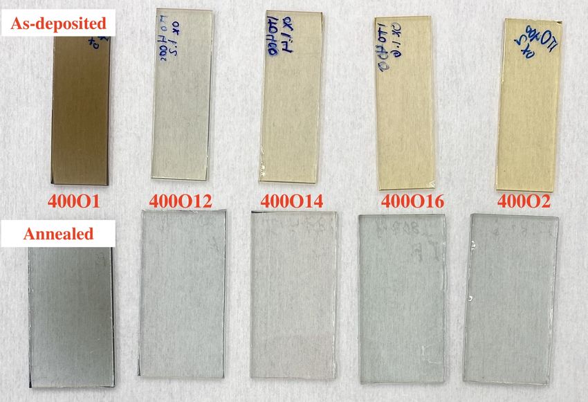
Uppsala University logotype

                          Sputtered Transparent Contact Layers for Bifacial and Tandem
                          Solar Cells
                          Klara Kiselman

Abstract
A key to solar cells with lower environmental impact is higher efficiency and reduced material
usages. Bifacial solar cells may have a higher efficiency as light can enter from two directions
and tandem solar cells may use a larger part of the incoming solar spectrum, increasing the
efficiency. However, both these applications require transparent and conducting contacts. This
thesis aimed to investigate how suitable the transparent conductive oxides aluminum doped
zinc oxide (AZO) and indium doped tin oxide (ITO) are as contacts in bifacial CIGS cells or
CIGS/Silicon tandem cells. The contacts must remain stable when CIGS is deposited on top of
it, meaning that they have to endure first 500°C and then 600°C in combination with copper,
indium, gallium and selenium vapours. A thin layer of AZO topped with ITO and pure ITO films
of different thicknesses were deposited by RF- and DC-sputtering, varying the oxygen flow.
Opto-electrical characterization showed that the transparency in the infrared was balanced
against high conductivity due to a shift in the plasmon peak's position. No great difference was
seen between pure ITO samples and AZO/ITO samples, so only the first where further
processed. The ITO films were annealed to 500°C in the CIGS deposition chamber, exposed to
selenium vapour. The films' sheet resistances dropped drastically, which was mainly attributed
to activation of tin donors. ITO produced with low oxygen flows also appeared more crystalline
according to x-ray diffraction measurements. Photon absorption in the ITO was used to estimate
the current loss in bifacial and tandem applications and graphs with current loss and sheet
resistance can be used to select an ITO deposition process. Commercial ITO was exposed to
100s of the CIGS deposition process but only during selenium and gallium vapour. A layer of
gallium selenide could be identified on the surface, but the ITO appeared to remain stable.
Sodium fluoride pre deposition treatment lowered the samples absorption for all wavelengths
compared to non-treated samples.

                                          Faculty of Science and Technology, Uppsala University. Place of publication eg Uppsala/Visby. Supervisor: Marika Edoff, Subject reader: Tobias Törndahl, Examiner: Tomas Nyberg

                           Faculty of Science and Technology
              Uppsala University, Place of publication eg Uppsala/Visby

                        Supervisor: Marika Edoff Subject reader: Tobias Törndahl
                                       Examiner: Tomas Nyberg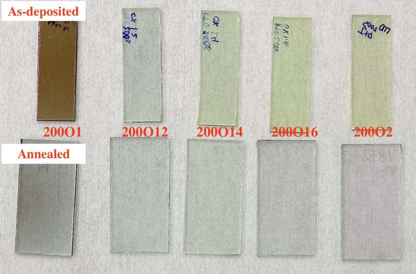
Populärvetenskaplig sammanfattning
Trots vetskapen om klimatförändringarna och dess allvarliga konsekvenser pro-
duceras majoriteten av världens elektricitet icke-förnybart. Solceller har enorm
potential att förändra detta - varje dag träffas jorden av samma mängd energi som
vi gör av med på ett helt år. Två nycklar till mer miljövänliga och kostnadseffek-
tiva solceller är högre producerad effekt per cell och mindre materialåtgång. Högre
effekt går bland annat att nå genom att konstruera dubbelsidiga celler, solceller
där ljus kan nå in genom både fram och baksidan. Samma förbättring fås med
tandemsolceller där två solceller som absorberar olika delar av ljusets våglängder
sätts på varandra. En solcell består förutom av det ljusabsorberande lagret också
av fram och bakkontakter som leder ut elektronerna i sidled. I dubbelsidiga och
tandemsolceller krävs att dessa kontakterna är transparenta.
Bakkontakten i CIGS tunnfilmssolceller är gjord av ogenomskinlig molybdenum
som då alltså behöver ersättas av en transparent ledare som klarar av den extrema
miljön i CIGS-processen. Framkontakten består redan nu av transparenta ledande
oxider, men i en tandemsolcell med CIGS och kisel behöver den också klara av att
CIGS läggs ovanpå dem. Det ljusarbsorberande CIGS-lagret läggs på i en vaku-
umkammare där temperaturen först höjs till 500 ◦C och sedan 600 ◦C när förångnin-
gen av koppar, indium, gallium och selen startar. Arbetet som presenteras i denna
rapport har gått ut på att med hjälp av sputtring tillverka tunna filmer av tenn
dopad indiumoxid (ITO) med olika tjocklek och syrehalt och sedan värma dem
till 500 ◦C. Dessutom utsattes kommersiell ITO för förångad gallium och selen
i 100 s och sedan 600 ◦C. Alla filmer karaktäriserades med spektrofotometri och
fyrpunktsprobsmätningar för att mäta absorption och lateral resistans.
För att nå ITO filmer med låg absorption i infrarött och hög lateral ledningsför-
måga behöver syremängden i dem optimeras. ITOs fria ledningselektroner kommer
från syrevakanser i kristallstrukturen och tenn som tar indiums plats. Mycket syre
ger få vakanser och sämre ledningsförmåga men också låg infraröd absorption,
eftersom att få fria laddningsbärare placerar plasmonpeaken i absorptionsspek-
trat bortom det infraröda. Plasmoner är oscillationer av fria laddningsbärare vars
resonansfrekvens ger en absorptionspeak. Efter värmning till 500 ◦C minskade re-
sistansen drastiskt för alla filmer, troligen på grund av att tenn aktiverades och
för den ITO med minst syre en högre grad kristallisering. Absorptionen ökade
dock i de flesta fall, men inte i alla. Genom att anta att en foton som absorberas
i kontaktlagret motsvarar en förlorad elektron i den utgående strömmen uppskat-
tades strömförlusterna i tandem och dubbelsidiga celler. Det var då tydligt att
en ITO motsvarande kommersiell ITO hade producerats. Den kommersiella ITOn
var stabil i 600 ◦C men ett tunt lager av galliumselenid la sig på toppen.
Contents
1 Introduction                                                                                                                   1
  1.1 Previous Research . . . . . . . . . . . . . . . . . . . . . . . . . . . .                                                  3
  1.2 Aim . . . . . . . . . . . . . . . . . . . . . . . . . . . . . . . . . . .                                                  5

2 Theory                                                                                                                         6
  2.1 Transparent Conductive Oxides . . . .                     .   .   .   .   .   .   .   .   .   .   .   .   .   .   .   .    6
      2.1.1 Annealing . . . . . . . . . . . .                   .   .   .   .   .   .   .   .   .   .   .   .   .   .   .   .    8
  2.2 Solar Cells . . . . . . . . . . . . . . . .               .   .   .   .   .   .   .   .   .   .   .   .   .   .   .   .    8
      2.2.1 TCOs in CIGS Solar Cells . . .                      .   .   .   .   .   .   .   .   .   .   .   .   .   .   .   .   12
  2.3 Laboratory Methods . . . . . . . . . .                    .   .   .   .   .   .   .   .   .   .   .   .   .   .   .   .   15
      2.3.1 Sputtering . . . . . . . . . . . .                  .   .   .   .   .   .   .   .   .   .   .   .   .   .   .   .   15
      2.3.2 Four Point Probe Measurements                       .   .   .   .   .   .   .   .   .   .   .   .   .   .   .   .   16
      2.3.3 Optical Characterisation . . . .                    .   .   .   .   .   .   .   .   .   .   .   .   .   .   .   .   17
      2.3.4 X-ray Diffraction . . . . . . . .                   .   .   .   .   .   .   .   .   .   .   .   .   .   .   .   .   18

3 Experimental                                                                                                                  22
  3.1 Deposition . . . . . . . . . .    .   .   .   .   .   .   .   .   .   .   .   .   .   .   .   .   .   .   .   .   .   .   22
  3.2 Characterisation . . . . . . .    .   .   .   .   .   .   .   .   .   .   .   .   .   .   .   .   .   .   .   .   .   .   23
  3.3 CIGS Deposition . . . . . .       .   .   .   .   .   .   .   .   .   .   .   .   .   .   .   .   .   .   .   .   .   .   24
  3.4 Estimation of Current Loss .      .   .   .   .   .   .   .   .   .   .   .   .   .   .   .   .   .   .   .   .   .   .   26

4 Method                                                                                                                        27

5 Results                                                                       29
  5.1 Effect of Annealing . . . . . . . . . . . . . . . . . . . . . . . . . . . 30
  5.2 Evaluation of ITO as Solar Cell Contact . . . . . . . . . . . . . . . 36

6 Discussion                                                                                                                    41
  6.1 ITO Films     Before Annealing . . . . .              .   .   .   .   .   .   .   .   .   .   .   .   .   .   .   .   .   41
  6.2 ITO Films     After Annealing in 500 ◦C               .   .   .   .   .   .   .   .   .   .   .   .   .   .   .   .   .   41
  6.3 ITO Films     After Annealing in 600 ◦C               .   .   .   .   .   .   .   .   .   .   .   .   .   .   .   .   .   42
  6.4 Outlook .     . . . . . . . . . . . . . . .           .   .   .   .   .   .   .   .   .   .   .   .   .   .   .   .   .   42

7 Conclusion                                                                                                                    44

A Deviation of Sheet Resistance Measurements with Four Point
  Probe                                                      49

B Corrections to Optical Measurements                                                                                           50

C Raw data                                                                                                                      51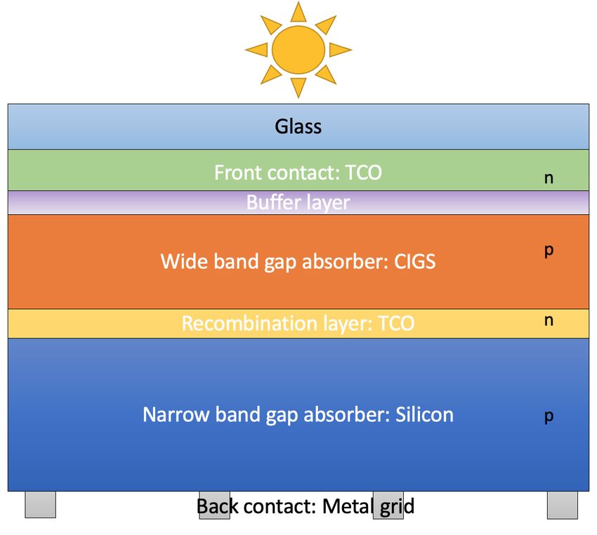
List of Abbreviations

AZO     Aluminium doped zinc oxide
CIGS    Cu(In, Ga)Se2
CB      Conduction band
CBM     Conduction band minimum
DC      Direct current
FF      Fill factor
FWHM    Full width half maximum
GIXRD   Grazing incidence x-ray diffraction
IOH     Hydrogen doped indium oxide
TCO     Transparent conductive oxide
ITO     Tin doped indium oxide
RF      Radio frequency
VB      Valence band
VBM     Valence band maximum
XRD     X-Ray diffraction
1    Introduction
Humanity is facing a crucial challenge that will define the future of our society -
climate change. The Intergovernmental Panel on Climate Change (IPCC) states
that the average global temperature had already increased by 1 ◦C in 2017 (com-
pared to pre-industrial levels) and a continued rise is associated with more extreme
weather events, rising sea levels and other devastating consequences [1]. Even so,
the main global energy sources remain non-renewables [2]. A rapid change is both
needed and ongoing and one of the renewable energy sources with great potential
is solar energy. Every hour, Earth’s atmosphere is hit by almost the same amount
of energy as the total annual global energy consumption [3]. This solar energy can
be converted to electricity by photovoltaics, solar cells. Even though solar electric-
ity contributes to no green-house gas emission during operation, the production
of the cells still affects the environment. The most common type of solar cells is
based on crystalline silicon with efficiencies of 24-26% in labs and just over 20%
in produced modules [4]. Two keys to decrease the environmental impact of solar
cells per produced kW h are increased efficiency and decreased material usage.
One way to increase the efficiency is to construct bifacial solar cells, i.e cells where
light can enter from two sides of the cell. This increases the amount of photons
that reach the absorbing layer and hence the generated current. If the absorber
is thin enough, it would also be possible to use these cells in applications such as
solar cell windows. A structure of a bifacial cell based on Cu(In, Ga)Se2 (CIGS)
is shown in Figure 1. CIGS is in this case the absorber where photons excite
electrons to become conductive. These electrons leave positive holes behind and
both are referred to as charge carriers. If the electron and hole pairs are not
separated, they will eventually recombine and do not contribute to the generated
current. Therefore, a pn-junction is used to drive the carriers out of the absorber,
and conductive contacts are needed to transfer electrons out to the cell’s edges.
There, a metal grid takes over and the circuit may be closed. Further elaboration
of the function of the layers in Figure 1 will be done in section 2.2. In order for
the cell to be bifacial, both the back and front contacts have to be transparent, in
contrast to the common CIGS configuration where opaque molybdenum is used as
the back contact.

                                           1
Figure 1: Structure of bifacial CIGS cell with a back and front contact TCO. The
n-p structure is needed to extract carriers out of the absorber.
All solar cells are limited by the absorbing material’s band gap, the minimum
energy needed to move an electron from the valence to the conduction band. Pho-
tons with too little energy will not be absorbed by the cell and hence generate
no current, while all photons with energy higher than the band gap can excite
electrons. This can be utilised to improve the efficiency by constructing tandem
devices, putting one solar cell on top of another. If the top cell has a wide band
gap, the low energy photons will continue down through the structure and be ab-
sorbed by the narrow band gap material in the bottom. In this way, a larger part
of the solar spectra is utilised, illustrated in Figure 2.
Figure 2: Schematic illustration of how a tandem solar cell uses a larger part of
the solar spectrum by using two absorbers with different band gaps.
2Since silicon based solar cells already account for 95% of the market [4] and have
a narrow band gap of 1.1 eV (photons with wavelengths up to 1127 nm is ab-
sorbed) [5], silicon is a great alternative for the bottom cell. A thin film solar
cell based on CIGS has a tuneable band gap of 1.1 to 1.7 eV and only a 1-2 µm
thin absorbing layer [3], which makes it suitable for the top cell. This thickness
can be compared to the around 200 µm needed for silicon cells [6]. It is believed
that silicon can not withstand the harsh conditions during CIGS deposition, so the
CIGS cell has to be deposited top to bottom and then laminated together with
the silicon cell. The two cells could also be connected such that the back contact
of CIGS and front contact of silicon is the same, known as a recombination layer.
Deposition of the front contact first is opposite to common CIGS cells’ deposition
processes and the structure is known as superstrate cells. In this way, both the
contact layers and thin film absorber can be deposited directly on the already
existing cover glass for silicon cells so that the total material usage decreases.
A sketch of the proposed tandem structure can be found in Figure 3 and deeper
description of the layers will be done in section 2.2. It is important to note that
the set up requires the front contact to withstand the high temperature (up to
600 ◦C) and exposure to copper, indium, gallium and selenium vapour as these are
the conditions of CIGS deposition. The junction has to be ohmic so that charge
carriers can flow between the layers and the material has to remain both conductive
and transparent, to minimise losses. Popular materials with these properties, at
least in normal conditions, are transparent conductive oxides (TCOs) [7, 8]. The
middle layer TCO does not have to provide high lateral conductivity but it has
to enable recombination of holes from CIGS and electrons from the silicon while
being transparent for low energy photons.
1.1 Previous Research
Tin doped indium oxide (ITO) and aluminium doped zinc oxide (AZO) are the
most popular transparent conductive materials used as front contacts, also referred
to as window layers, in thin film solar cells [9]. Nakada et al. did the first study
of TCO back contacts for solar cells in 2004, using AZO, fluorine doped tin oxide
(FTO) and ITO [10, 11]. These materials remain the most studied alternatives
for transparent back contacts but problems with the back contact junction occur
during high temperature (>500 ◦C) depositions of CIGS [12]. This leads to cells
with less efficiency. However, Nakada et al. were able to reach CIGS solar cells
performing well when the temperature of the CIGS deposition process was kept
below 520 ◦C. Above that temperature, they found a thin layer of gallium oxide
(Ga2 O3 ) in the ITO/CIGS interface to be the source of lower efficiency. This n-type
3Figure 3: Proposed CIGS-silicon tandem cell. The front contact, buffer layer,
CIGS and recombination layer can be deposited in that order (front contact →
buffer layer → CIGS → recombination layer) on the cover glass and then laminated
together with the silicon. CIGS absorbs the high energy photons and silicon the
remaining low energy photons. The n-p-n-p structure is needed to extract charge
carriers.
semiconductor opposes carrier transport and hence the efficiency is lowered. In
contrast, Son et al. found gallium oxide to be present even though the temperature
was kept below 420 ◦C [13]. They also found the thickness of ITO to correlate
with the thickness of the gallium oxide layer, which made the barrier wider. [13].
Saifullah et al tried, and succeeded, to decrease the amount of gallium oxide by
incorporation of sulfurized-AgGa in between ITO and CIGS [14]. A thin layer
of molybdenum was used by Nakada et al., but the resulting transparency was
never reported [10].
Son et al. found that sodium present during CIGS deposition may introduce
defects in the gallium oxide layer, improving the junction [13]. Sodium treatments
on CIGS absorbers are used to increase the CIGS doping concentration and hence
the efficiency. In addition to pre or post deposition treatments, sodium may diffuse
from soda lime glass substrates. Keller et al used hydrogen doped indium oxide
(IOH) as back contact for CIGS and suggested that it may hinder the diffusion
of sodium, and that the thicker the IOH layer the less sodium hence lower doping
in the CIGS [12]. Other studies using ITO have however not found this [10, 15].
For a cell configuration such as the proposed tandem structure in Figure 3 the
4problems in the TCO/CIGS interface are not relevant since the ITO will be covered
with a buffer layer prior to CIGS deposition (this interface is however equally
problematic). For bifacial applications (Figure 1), they are.
ITO and AZO films can be prepared in many ways, for example by magnetron
sputtering, atomic layer deposition, sol-gel process, chemical vapour deposition or
pulsed laser deposition [16]. The front contact layer in CIGS is most often prepared
by magnetron sputtering [16], a well established technique to reach thin, homoge-
nous films [17]. However, direct translation from one sputter set up to another is
not straight forward due to the many degrees of freedom in the geometric config-
uration, the type of power supply and the sensitivity of the instruments. Mathias
Axelsson studied ITO and AZO deposition by the same sputter used in this thesis,
located in the Myfab cleanroom at the Ångström laboratory (Uppsala) [18].
Among other things, Axelsson investigated the lateral conductivity of the films.
Lateral resistance, sheet resistance, is measured in Ω/ and will be explained
in section 2.3.2, but it is crucial for a solar cell contact to be able to conduct
carriers out to the cell’s edges. Axelsson did not reach sheet resistances below
25 Ω/, which was obtained with a 215 nm thick ITO layer [18]. For this thesis,
10 Ω/ or lower was desired, so more exploration was needed. This benchmark was
selected based on that 10 Ω/ is the optimal value of front contacts of 5 mm wide
cells [19]. Regarding materials, ITO outperforms AZO in long-term stability and
conductivity but it has been seen that a 150 nm thick AZO layer can promote the
growth of more crystalline ITO, which improves the film’s electrical properties [16].
However, Gouillart et al found that an AZO layer as thin as 50 nm gave better
performance of reflective CIGS cells based on Ag/AZO/ITO back contacts [20].
1.2 Aim
The overall aim of this thesis was to develop a transparent contact for CIGS solar
cells to replace the current opaque molybdenum contact. The contact was thought
to be used as front contact or recombination contact in a tandem structure and
back contact in a bifacial structure. Therefore, the contact had to be transparent,
conductive and remain so when a buffer layer and/or CIGS was deposited on top
of it. CIGS deposition requires the contact to withstand 500 ◦C before exposed to
copper, indium, gallium and selenium vapours and then, as an initial CIGS layer
has formed on the surface, 600 ◦C. In addition, the electrical contact between
the materials has to be good. A TCO with sheet resistance below 10 Ω/ and low
absorption in both the visible and infrared range was desired. Since ITO and AZO
are often used as front contacts [9], these materials were chosen as candidates. AZO
was to be used as a thin layer underneath ITO to improve the ITO’s crystalline
structure.
52 Theory
This section will provide a background to subjects relevant for this thesis, including
theory of methods. Basic understanding of solid state physics is required.
2.1 Transparent Conductive Oxides
ITO (In2 O3 :Sn) is a n-type semiconductor and the most popular transparent con-
ductive oxide (TCO). Aluminium doped zinc oxide (AZO), also an n-type semicon-
ductor, has gained popularity in recent years since indium is a rare earth element
but aluminium is abundant. TCOs are widely used in electronics due to their
ability to be both transparent and conductive. This unusual combination of prop-
erties is a consequence of a shift in the energy band configuration, known as the
Moss-Burnstein shift. For a semiconductor to be transparent in the visible region,
the band gap has to be larger than the highest energy of visible light, >3.1 eV.
However, a wider band gap means that it is less probable to get charge carrier
excited into the conduction band (CB), where the carriers are needed in order to
conduct electricity. TCOs overcome this problem by widening the optical band
gap while keeping the conduction band partly filled, as can be seen in Figure 4.
With sufficient band alignment, the Fermi level is shifted upwards so that the CB
gets partly filled and the new optical band gap is given by
Egopt = EgM B + Eg = EF − EV BM . (1)
However, this is only true if the distance to the next conductive band (CB+1) is
larger than 3.1 eV. [7]
In an n-type TCO, the local excess of electrons originates from three types of
defects [7]. Oxygen vacancies results in non bonded valence electrons on the metal
ion and the same arises from interstitial metal atoms [7]. Doping with atoms with
higher valence than the metal gives free electrons, as do substitution of oxygen
to an atom with fewer valence electrons [7]. In ITO, the four valence tin replaces
the three valence indium. [7] However, there’s not enough energy provided in room
temperature deposited ITO-films for this substitution, so oxygen vacancies provide
almost the whole conductivity [17], while unincorporated tin increases the electron
scattering and hence reduces the mobility [8]. These films are also amorphous and
in order for ITO to be fully crystalline and tin to be included in the lattice,
temperatures of above 200 ◦C are needed [17]. Fully crystalline structures are
however only reached above 400 ◦C [17]. If ITO is produced by sputter deposition,
the needed energy can be come from kinetic energy of the atoms creating the film.
6Figure 4: Illustration of the Moss-Burnstein shift. EF shows the Fermi energy,
CBM the conduction band minimum, VBM the valence band maximum, Eg the
original band gap and Egopt the resulting optical band gap when using the energy
shift EgM B .
Charge carriers being present in the conduction band are not enough to get good
conductivity, they also have to have a high mobility. The conductivity σcond in
S/cm2 is given by
σcond = neµ, (2)
where n is the density of free charge carriers (electrons if n-type material), e the el-
ementary charge and µ the electron mobility. In order to enhance the conductivity
either the mobility or free charge carrier concentration can be increased. However,
higher concentration of charge carriers can give rise to optical absorption within
the conduction band. This absorption’s coefficient α is proportional to the free
electron density n according to
α = σabs n, (3)
where σabs is the absorption cross-section. Higher levels of doping does not only
give high absorption but also increases the electron scattering against defect (dopant)
sites in the crystal. Increased scattering may also rise from smaller crystalline sizes,
as electrons may scatter in the grain boundaries [21]. This reduces the mobility
and hence decreases the conductivity. [7]
Another consequence of higher doping is that the plasmon wavelength decreases.
Plasmons, or plasma oscillations, are collective oscillations of electrons in the con-
duction band. The higher dopant concentration N , the shorter the peak absorption
wavelength for plasmons is, illustrated in Figure 5 [22]. This phenomena puts a
trade off between the conductivity and the transparency in infrared [22]. This may
partly be counteracted by alternation of the peak’s amplitude, which is affected
by the electrons’ relaxation time. Large relaxation times, τ , are connected to high
mobility, µ and lower peak intensity [23].
7Figure 5: Schematic illustration of the plasmon peak wavelength’s λp dependency
on charge carrier concentration. The short wavelength absorption edge due to
absorption of photons with energies higher than the band gap is also illustrated.
2.1.1 Annealing
Annealing of ITO films in vacuum has been found to increase the crystallite size,
reducing the resistivity of the film rapidly above around 770 ◦C. The same change
was found for air annealed samples, but first an increase of resistivity occurred
due to oxidation, i.e. loss of free electrons. As previously mentioned, the tin is
inactive in the amorphous state but carriers are released during annealing. This
also lowers the scattering on tin impurities or tin oxide complexes, improving the
mobility. [24]
2.2 Solar Cells
For a general background to solar cells the reader is referred to The Physics of
Solar Cells by Jenny Nelson [25]. Some concepts important for this thesis are
however presented here.
In solar cells, a semiconductor’s ability to absorb light to form electron-hole pairs is
utilised. However, the generated electron and hole will recombine if not separated.
The mean length the pair travels before recombining is called the diffusion length
and the mean time the minority charge carrier lifetime. In order to counteract
the recombination and facilitate the extraction of carriers, an n-type and p-type
semiconductor are often combined. This shared interface is known as a pn-junction
where the n side’s free electrons diffuse to the holes on the p-side and the two
carriers cancel each other. At the same time, the moving electrons leave positive
8ions behind, creating an uneven charge distribution - an electric field. This electric
field works against the diffusion and eventually, equilibrium is reached. A pn-
junction is illustrated in Figure 6. [3]
Figure 6: Illustration of a pn-junction. Electrons from the n-side have diffused into
the p-side and recombined with holes, creating negative ions. As a consequence,
positive ions are left on the n-side and this charge difference creates an electric
field. The region where no free charge carriers are present is known as the depletion
region. The electric field creates a barrier for electrons to flow from the n- to the
p-side and vice versa for holes.
Majority charge carriers, i.e. electrons in the n-type materials and holes in the
p-type material encounters a potential barrier if they try to flow over the pn-
junction. This barrier may be lowered by applying a forward voltage. When the
forward biasing voltage reaches the value of the electric field, the additional applied
voltage will give a positive current that increases exponentially, just as a diode.
Under dark conditions, the solar cell follows equation 4 known as Schockley’s diode
equation for ideal diodes. There, J is the current density with the dark saturation
current (no applied voltage) value J0 and V the bias voltage. [3]
qV
J = J0 (e kT − 1) (4)
9However, CIGS solar cells’ absorbers are always p-type, so the photo generation
of an electron hole pair happens in a p-type semiconductor. The front contact is
then n-type and since the electron is a minority charge carrier on the p-side, it
will be transported across the depletion region by the built in electric field. This
holds given that it is generated within a diffusion length from the region, or inside
it. The energy band configuration of this transport is shown in Figure 7. [3]
Figure 7: Diagram of the energy bands’ bending in a pn-junction and illustration
of how an electron from a photo generated electron hole pair is swept across the
region driven by the electric field. The electron and hole are then separated and
recombination is avoided. In a solar cell with a p-type absorber, the front contact
is n-type and the photons enter the solar cell through it, without being absorbed.
When the solar cell is exposed to light but the back and front contacts are con-
nected with a load of 0 Ω, the resulting current is known as the short circuit current
Jsc . If the charges can not move out of the semiconductors, they will accumulate
on the back and front, giving a potential difference between the contacts named
the open-circuit voltage, Voc . The photo-generated current JL is negative com-
pared to the exponential diode current in equation 4, since electrons now travel
from the p to the n material. The total current as a function of applied voltage can
be approximated with the empirical one-diode model in equation 5, which corre-
sponding circuit is presented in Figure 8. In addition to the diode ideality factor A
describing the deviation from the ideal diode model it also takes the voltage over
a series resistance JRs and current through a shunt path Rsh into account. [3]
q(V −JRs ) (V − JRs )
J = J0 (e AkT − 1) + − JL (5)
Rsh
From measurements of J as a function of different bias voltages V one can obtain
Jsc , Voc , fill factor F F and efficiency η. Measurement curves may look like the
ones in Figure 9. Parameters can be extracted by simply reading the intersections
of the curve and the axes to get Jsc and Voc and the maximum power output Pmp
10Figure 8: The equivalent circuit of a solar cell under illumination but not con-
nected to a load. The photo generated current is JL and the pn-junction barrier
is represented as a diode. Series resistances Rs and shunt resistance Rsh affect the
output power.
from where the fill factor is calculated according to
Pmp Vmp Jmp
FF = = . (6)
Voc Jsc Voc Jsc
The fill factor can be thought of as how square the current-voltage curve (IV-curve)
is. A large one, i.e. a very square curve, is desired. Then, the efficiency is obtained
by dividing the output maximum power with the input power
Pmp Voc Jsc F F
η= = . (7)
Pin Pin
As is clear from equation 7, the efficiency depends on both Voc and Jsc . These
values are linked to the band gap. The open circuit voltage can not be higher than
the band gap and the short circuit current is limited by the amount of photons
with enough energy to excite electrons. Higher band gaps require higher energy
of the photons, hence less photons of the solar spectrum can be used and the
short circuit current decreases. The first derivation of the optimal band gap and
theoretical limit of the efficiency was done by Shockley and Queisser [26]. Based
on blackbody radiation of 6000 K a peak of 30.5% for a band gap of 1.35 eV, lately
adjusted to 33.1% for the sun spectrum after 1.5 atmospheres. However, these
values are calculated based on that i) the photon absorption is 100% when the
the photon’s energy is larger than the band gap, ii) radiative band-to-band is the
only occurring recombination, iii) radiative energy losses come from 300 K black
body radiation and iv) the cell is an ideal diode (A = 1). In order to overcome the
Shockley-Queisser limit one may combine solar cells with several absorbers with
different band gaps. In a tandem solar cell, two junctions will be present and a
greater fraction of the solar spectrum is used. [3]
112.2.1 TCOs in CIGS Solar Cells
CIGS solar cells are based on a a chalcopyrite crystal structure which can be made
both as n- and p-type by variation of intrinsic defects. For solar cells, the p-type is
used and the hole dopant charge carrier concentration arises from copper vacancies.
These vacancies are countered by indium or gallium anti-sites defects (replacing
copper) and selenium vacancies. To avoid the latter CIGS is grown in selenium
excess. Sodium has been found to increase the doping concentration both via
pre and post deposition treatments, improving the absorber’s performance. The
mechanisms behind this is however not fully understood. [3]
The components of a CIGS thin film solar cell are: substrate, back contact, p-type
absorber, n-type transparent front contact and a metal grid. The substrate is
commonly soda lime glass, the back contact molybdenum while the front contact
is made up of several layers. A buffer layer is used to reduce the recombination
rate at the surface and to create a good electric contact between the absorber and
front contact. Usually an intrinsic layer is used in between the buffer layer and the
transparent n-type front contact, which commonly is AZO. Since CIGS is p-type,
an n-type material is needed in the window layer to create a pn-junction. [3]
In addition, the junction between the contact and absorber has to be ohmic, mean-
ing the electrons have to be able to flow trough the covering contact layer out to
the side contacts. High resistance in the contact layers will contribute to the series
resistance Rs , in equation 5, lowering the output current. This makes Jmp and
Vmp decrease and as seen in equation 6 and 7, this leads to a lower fill factor and
efficiency. In an IV-curve, an increased series resistance will be seen as less squared
curve, illustrated in Figure 9 1 . Low lateral resistance is hence needed to increase
the cells’ efficency. TCO back contacts compete with todays molybdenum con-
tacts, typically with a sheet resistance of 0.6 Ω/ [27]. A transparent contact may
however counteract the loss due to series resistance, if it provides enough extra
photons either to its own cell or an underlying one.
1
Figure from: Squirmymcphee, CC BY-SA 3.0 https://creativecommons.org/licenses/
by-sa/3.0, via Wikimedia Commons. Added Jmp, Vmp and the square illustrating the FF.
12Figure 9: Plot showing how the current voltage characteristics of a solar cell
following equation 5 is affected by the series resistance. The higher the series
resistance the less square the curve appears, which lowers the FF by reduction of
Jmp and Vmp . The Jmp and Vmp for the curve with 1 Ω is marked.
If an n-type TCO, such as ITO or AZO, is used as back contact, a pn-junction
is achieved, but in the opposite direction compared to the one used to extract
electrons in the front contact. It is not desirable that electrons move towards the
back contact, as this would create an opposite current. Instead, holes should move
to the back contact and recombine with incoming electrons to close the circuit. A
band diagram of an ITO/CIGS interface is showed in Figure 10. It is constructed
based on electron affinity 4.5 eV and band gap 1.1 eV for CIGS and work function
4.7 eV and band gap 3.4 eV for ITO [28]. The fermi levels have to be connected,
since no voltage drop occurs over the interface. Both the ITO and CIGS band
gap and ITO electron affinity may be altered, so the band diagram should just be
thought of as a schematic one. The strength of the band bending is also affected
by the doping concentration in both materials. Nevertheless, the figure shows how
the electrons and holes can recombine either by tunnelling through the barrier, or
jumping via defect states in the interface. Gallium oxide is not included in this
band diagram, but it is probable that this n-type semiconductor would cause a
larger barrier for the recombination.
13Figure 10: Band diagram of ITO/CIGS interface based on CIGS with an electron
affinity of 4.5 eV and band gap of 1.1 eV meeting ITO with a work function of
4.7 eV and band gap of 3.4 eV. The bands and their interfaces are first constructed
with the vacuum energy level as constant and the notches then occur as the fermi
levels of the materials are aligned.
142.3 Laboratory Methods
The following section contains theory of laboratory methods used in this thesis.
2.3.1 Sputtering
Sputtering is the main technique used to deposit thin homogenous films. Ions
bombard a target material, who’s atoms are ejected and create a homogenous
film. First, the deposition chamber is pumped down to a base pressure, removing
undesired gases. Then an inert, pure process gas (commonly argon) fills the cham-
ber. By applying a strong negative voltage to the target, it becomes a cathode and
the opposite substrate becomes an anode. The argon gas is electrically excited to
plasma and the positive argon ions bombard the negative target. Target atoms are
then ejected and condense to a thin homogenous film on the substrate opposite to
the target. In reactive sputtering an additional gas is introduced, reacting with
the atoms in the growing film. For TCOs, oxygen is often added to get appropriate
oxygen amounts within the films. [29]
Variation of the power supply gives either direct current (DC) sputtering where the
potential diffrent between anode and cathode is constant or radio frequency (RF)
sputtering, where it alternates with 13.56 MHz. RF sputtering is preferred if the
target is non conductive, but ceramic ITO targets provide enough conductivity and
DC sputtering is hence most common as the deposition rate is higher. In addition
a magnetron is often used, creating a magnetic field to contain the plasma by
the target. For TCOs, ceramic targets are preferred over metallic since the later
is associated with ’poisoning’ [8], i.e. the thin film is not only deposited on the
substrate but also on the target. The whole process and working point of the
sputter is hence more controllable with ceramic targets. A schematic illustration
of DC magnetron sputtering is shown in Figure 11. [17]
Parameters that can be varied in the sputtering deposition process include de-
position time, sputtering power and pressure, flow of process gas and heating of
substrate. The deposition time is in general directly proportional to the thickness
of the film while the other parameters influence the crystallisation. High mobility
through better grain structure can be achieved by high temperature during deposi-
tion or annealing afterwards. By higher pressure the energy of the free target atoms
is reduced, which can lead to amorphous films and hence more electron scattering
and lower conductivity. For ITO, Secouard et al. showed that the transmission
in the infrared range increases with the oxygen flow during reactive magnetron
sputtering. This is attributed to decreasing amount of charge carriers as oxygen
vacancies are filled and tin’s deactivation as it forms complexes with oxygen. [30]
15Figure 11: Illustration of DC magnetron sputtering of some target material (or-
ange) using argon (blue) as process gas.
2.3.2 Four Point Probe Measurements
In thin film technology the lateral conductivity of a film is often out of interest.
For a solar cell contact, the transport of charge carriers from the absorbing layer
out to the conducting grid is very important, hence the lateral resistance is used
for characterisation. This resistance - sheet resistance - is independent of the area
of the film. Defined as the ratio of conductivity and thickness, Rs = ρt the unit is
Ω but in order to distinguish the sheet resistance from regular resistance, the unit
Ω/ is used. Note that sheet resistance is inversely proportional to the thickness,
so that a halving of thickness gives twice the sheet resistance.
In order to measure the sheet resistance, a four point probe it used. It has four
probes commonly equidistanced along a line, where the outer probes conduct the
current I, as illustrated in Figure 12. The two inner probes measure the poten-
tial difference ∆V and if the probe is not near any edge of the sample and the
thickness less than 40% of the distance between the probes, the sheet resistance is
16calculated by
π ∆V ∆V
Rs = = 4.53236 . (8)
ln 2 I I
A more detailed derivation of this equation is presented in Appendix A. The advan-
tage with a four terminal configuration is that the wire and contact resistance for
probe 2 and 3 (R2 and R3 in Figure 12) does not influence the voltage measurement
since no current flows through these probes. [31]
Figure 12: Schematic illustration of a four point probe where the probes are dis-
tanced by s and the flowing current illustrated by blue arrows.
2.3.3 Optical Characterisation
The main optical properties of interest for thin films are the wavelength dependent
transmittance, T and reflectance, R. From these values, the absorbance A is
calculated via
A = 1 − T − R, (9)
given that all values are normalised to the intensity of the incoming light. The total
absorbance of a thin film with thickness d is proportional to (1−eαd ), but if α and d
are small, Taylor expansion gives (1−eαd ) = 1−(1−αd)+ 12 (1−αd)2 +... ≈ αd. [19]
17In this thesis, transmittance and reflectance of each sample were measured using
spectrophotometry with an integrating sphere. Since the optical properties usu-
ally are wavelength dependent, a monochromator is used before the light hits the
sample. The total transmitted or reflected light is then collected by the integrating
sphere. The sphere’s inside is coated with a highly reflective coating against which
the light is reflected multiple times before it encounters the detector. In this way,
all light is collected and then compared to the intensity of a reference beam. [32]
An even more sensitive optical method is spectroscopic ellipsometry, where the
change in light’s polarisation is measured. A model of various oscillators is then
constructed to match the measured changes. From these models, material con-
stants such as the refractive index n, extinction coefficient k and the permittivity
can be read. The stronger the permittivity of a material is, the more the mate-
rial’s charge distribution align with an applied electromagnetic field. It has a real
part 1 and imaginary part 2 which are frequency dependent. If the Drude model
is used to model the oscillations of electrons, these parameters have the values [33]:
ωp2
1 = 1 − (10)
ω2 + γ 2
and
ωp2 γ
2 = . (11)
ω(ω 2 + γ 2 )
Here, ω is the frequency of the incoming light and γ the damping of oscillations
within the material. The damping is the inverse of the relaxation time τ , γ =
1/τ . The plasma frequency ωp is the resonance frequency of the free electrons in
the material, directly related to the plasmon wavelength λp discussed in previous
sections [33]. As ω → ωp , 1 → 1 − 1+γ12 /ω2 ≈ 0 if γthe interfering x-rays are in phase or not. Constructive interference occurs if the
difference in the traveled distance between the rays is a multiple of the wavelength.
This gives a condition for the distance between reflective planes that is described
by Bragg’s law, equation 12. There, n is any integer, λ the wavelength of incoming
radiation, d the interatomic distances and θ the incident angle. The angle between
incident and outgoing rays will in this case be 2θ. As illustrated in Figure 132 , the
lower ray will travel a distance of 2d sin θ extra compared to the upper one. [34]
nλ = 2d sin θ (12)
Figure 13: Illustration of Bragg’s law of diffraction in a simple 2D lattice with a
distance d between the planes. The light’s incident angle is θ
Every constructive interference point is associated with a set of planes within the
crystal structure. A set of these planes has to contain all lattice points. In real
space, the planes are described by their miller indices hkl. Miller indices are the
points of the plane’s intersection with the unit cell’s axes multiplied with a factor
to obtain only integer values. For a cubic lattice with lattice constant (side length)
a, the distance between the planes in set hkl can be calculated as
a
dhkl = p , (13)
h2 + k 2 + j l
while the equations are more complex for other crystal structures. [35]
During XRD θ/2θ measurements, the incident angle is varied and the angle 2θ
measured while the wavelength is constant. All angles are measured with respect
2
Source: Hydrargyrum, CC BY-SA 3.0
https://creativecommons.org/licenses/by-sa/3.0, via Wikimedia Commons
19to the samples’ surface. If the sample is fully crystalline, distinct peaks will appear where Bragg’s law is fulfilled. The peaks’ positions will then translate into sets of planes present in the crystal structure and when all sets are known, into a full structure. The measured diffractogram is compared to previously determined (experimental or theoretical) possible patterns and their crystal structures, taking into account that several set of planes can give the same Bragg angle. [35] For thin films, grazing incident XRD (GIXRD) is preferred over symmetric θ/2θ scans. In θ/2θ scans, a thin sample will allow x-rays to penetrate the substrate, which reflections will be measured by the detector. To avoid this and to increase the intensity of the signal, GIXRD keep the incident angle small and only the detector changes its position, illustrated in Figure 14. The method assumes a randomly oriented crystal not perfectly aligned with the substrate. [35] Figure 14: Schematic, 2D image of GIXRD on a thin film with incident angle α and measured angle 2θ − α. α is however so small (
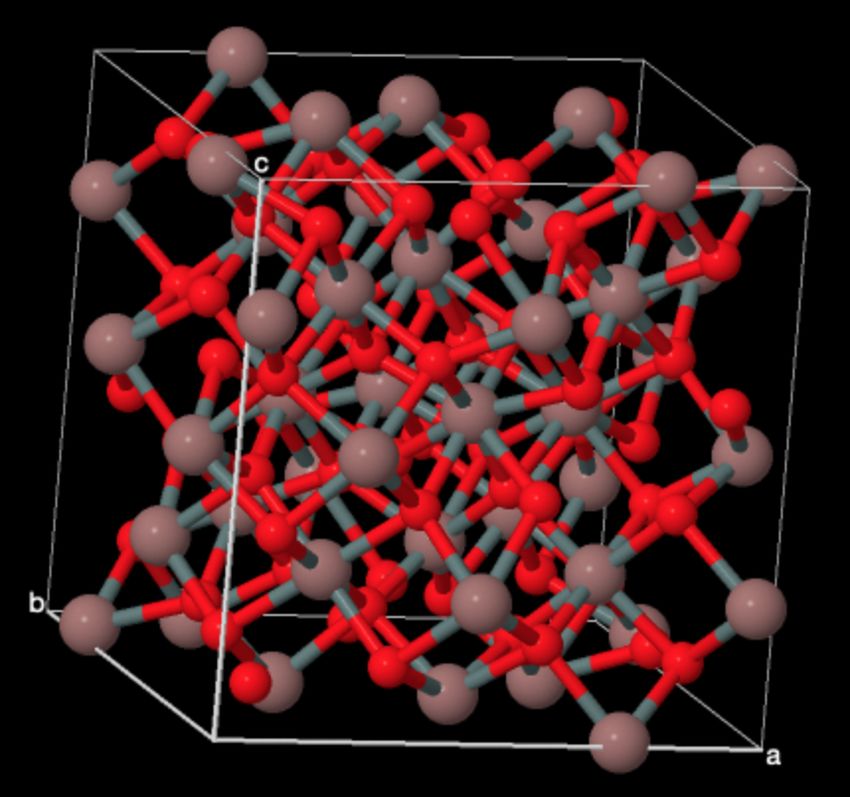
Figure 15: 3D image of indium tin oxide’s unit cell in the bixbyite structure.
Animation by ICSD [36] based on data from Gonzalez et al’s study by neutron
powder diffraction [37]. Oxygen in red and indium in brown. Tin doping replaces
part of the indium with tin.

                                      21
3 Experimental
All different AZO/ITO samples in this thesis were deposited on 2 mm thick soda
lime glass substrates that were ultrasonic cleaned by a Steelco US 80. Every
deposition run also included a dummy piece of soda lime glass of 1.7 mm, which
were not processed any further and hence used for characterisation of as-deposited
properties.
3.1 Deposition
For deposition of AZO and ITO a von Ardenne CS730 sputter was used. AZO
was sputtered using RF magnetron sputtering while ITO was deposited using DC
magnetron sputtering. Used targets had a diameter of 200 mm positioned 55 mm
from the substrate. The ITO had a composition of 90:10 In2 O3 to Sn2 O3 with
99.99% purity and AZO of 2% weight Al2 O3 with 99.99% purity. Unchanged set-
tings for AZO deposition is presented in Table 1 and constant parameters for ITO
in Table 2. The unit sccm stands for standard cubic centimetres per minute during
standard temperature and pressure, so it is related to molar flow rate. A fraction
between two sccm flows then gives a molar fraction. Before deposition the target
was presputtered for 1 min in the same conditions used when the shutter opened,
to minimise the risk of memory effects such as oxygen stored in the chamber walls.
In addition, the order of the samples was randomised.
Table 1: Parameters for RF magnetron sputtering of AZO.
Power 640 W
Working pressure 6 mbar
Argon flow 80 sccm
Oxygen flow 0.4 sccm
Extra heating No
Deposition time 75 s
Table 2: Constant parameters for DC magnetron sputtering of ITO.
Power 640 W
Working pressure 6 mbar
Argon flow 40 sccm
Extra heating No
223.2 Characterisation
All deposition runs were done with one dummy piece for sheet resistance and one
piece partly covered by caption tape. The latter was used to measure the layers’
thicknesses on three different places using a stylus profiler Dektak 150. The sheet
resistance of all samples were obtained with a four-point probe (CMT-SR2000N).
In addition, transmission and reflection between 300 and 1300 nm with step size
5 nm were measured using PerkinElmer LAMBDA 900 spectrophotometer with
integrating sphere for all samples except the first run of AZO/ITO films. For
those samples the step size was 10 nm and the maximum wavelength 2500 nm.
If samples were too small to cover the whole beam, an aperture was used and
corrected for according to Appendix B. Calibration of reflection measurements
up to 1000 nm was preformed using a silicon wafer. Above that, a mean of the
wavelength dependent correction value was used. Reflection and transmission gave
absorption via equation 9, where the measured absorption of the substrate glass
was subtracted. The absorption of the thinner glass (1.7 mm) is shown in Figure16.
Figure 16: Measured absorption of substrate glass, used for correction of measure-
ments. The soda lime glass appears to have a band gap around 350 nm.
Furthermore, XRD was preformed on four samples to deduce their crystal struc-
ture. A short θ/2θ scan and GI scan showed similar results, so GIXRD with an
incident angle of 1◦ was selected (after evaluation of the critical angle). 2θ was
varied from 15◦ to 75◦ in steps of 0.27◦ with five seconds data collection per step.
In addition, the annealed 120O1 sample was subject to spectroscopic ellipsometry
23measurements. Wavelength was varied from 210 nm to 1700 nm with steps of 5 nm.
Incident angles of 60◦ , 65◦ and 70◦ were used and a model was fitted to the com-
bined result. The fitted model consisted of one Drude oscillator, one parametric
semiconductor oscillator and one gaussian oscillator with mean square error 33.
3.3 CIGS Deposition
Fabrication of CIGS is in the Ångström laboratory done by co-evaporation of el-
ements in boat sources. The process is controlled by mass spectrometer feedback
and relative rates of the different elements are shown in Figure 18. Selenium is
provided in excess and the ratios between all elements are alternated to obtain a
CIGS layer with lower electron density close to the back contact, limiting the back
contact recombination. After reaching a pressure of 10 × 10−6 mbar but before
deposition of CIGS the substrate temperature is increased up to 500 ◦C and the
temperature of the selenium source up to 380 ◦C. During the process the tem-
perature of the samples reaches about 600 ◦C, shown in Figure 17. The whole
deposition lasts for 1600 s. Incorporation of sodium for higher doping is commonly
done by precursor layers of sodium fluoride (NaF). It is deposited by thermal evap-
oration (Luxel Radak II) using a boron nitride liner in a separate vacuum system.
Thickness is controlled by a quartz crystal monitor so that an approximately 20 nm
thin layer NaF is achieved.
Figure 17: Temperature of the graphite plate heating the substrate (black) and
the selenium source (blue) during CIGS deposition. The x-axis shows the time in
seconds and grey areas mean that the shutter in front of the samples is closed and
white that it is open. The actual temperature of the substrates is not known but
it is estimated to be about 50 ◦C lower than the graphite plate.
24Figure 18: Relative rates of the concentration of copper (red), indium (blue), gal-
lium (green) and silver (orange) in a standard deposition process for (Ag, Cu)(In,
Ga)Se2 solar cells. In this study, no silver was incorporated so the copper ratio was
the sum of the copper and silver rates. Rates shown here are the signals from the
mass spectrometer so the instruments varying sensitivity for different elements is
taken into account (why indium is higher). The x-axis shows the time in seconds
and grey areas means that the shutter in front of the samples is closed while the
background is white if it is open.
253.4 Estimation of Current Loss
A figure of merit for the transparent contacts was defined as the current loss in the
solar cell due to photon absorption in the contact. It was approximated that every
lost photon lead to a lost electron in produced current, which is an overestimation
of the efficiency in the absorber. Since the energy distribution of photons emitted
by the sun isn’t uniform and certain wavelengths are absorbed by elements in
the atmosphere, the current loss is wavelength dependent. To account for this,
American Society for Testing and Materials’ (ASTM) G-173 spectra with global
tilt after interaction with 1.5 atmospheres was used. This spectra is illustrated
in Figure 19 [38]. It shows the irradiance per square meter and wavelength for a
surface perpendicular to the sun.
The spectra was multiplied with the absorption (per wavelength) of the contact
and after unit conversions integrated over a selected wavelength interval. Matlab’s
built in trapezoidal method was used for this, with step size 5 nm as this was
the interval used during optical measurements. For bifacial applications or usage
of the TCO as front contact in a tandem structure, the whole interval in which
CIGS may absorb photons was used, i.e. integration limits were set to 1.1 eV to
4 eV (1127 nm to 310 nm). When the TCO is used as the recombination layer in a
tandem structure, photons with lower energy than silicon’s band gap will not be
absorbed by the cell. Therefore, integration limits were then set to 1.1 eV to 1.5 eV
(1127 nm to 827 nm). The amount of photons was then converted to current loss
per cell area.
Figure 19: ASTM G-173 Global tilt AM 1.5 irradiance spectra from a 37◦ tilted
area facing the sun.
264 Method
Since the sheet resistance of a film is inversely proportional to the thickness of
the film, deposition time was chosen as one of the main parameters to investigate.
Thicker films give higher lateral conductivity, so long deposition times of 200 and
400 s were selected. In addition, oxygen flow was varied since the oxygen has a
large influence on the conductivity and transparency of ITO [8]. A matrix with
four different settings was constructed as in Table 3 to get an idea of the process
boundaries. Two different samples of each setting were produced, one with only
ITO and one with ITO on top of AZO. A similar AZO thickness as the one used by
Gouillart et al for reflective back contacts (50 nm) [20] was the aim. The samples
with AZO bottom layer were named in the same way as pure ITO samples, but
with an A in front. For example, A200O1 refers to a sample with ITO produced
according to Table 3 on top of a thin layer of AZO manufactured as in Table 1.
Table 3: Varied parameters for DC magnetron sputtering of ITO.
Sample O2 flow, absolute O2 flow, ratio Deposition time
200O1 1.0 sccm 2.44% 200 s
400O1 1.0 sccm 2.44% 400 s
200O2 2.0 sccm 4.76% 200 s
400O2 2.0 sccm 4.76% 400 s
Evaluation of the first results (see Appendix C) came to the conclusion that AZO
may provide a better ground for ITO to grow on, but that this effect diminished
with thicker samples. In addition, the sheet resistance of the thin AZO layer was
above 500 Ω/ so it did not contribute to a lower sheet resistance via a parallel
connection. The samples with higher oxygen flow had lower absorption in the
infrared range but higher sheet resistance compared to the samples produced with
1 sccm oxygen. Therefore, more samples with oxygen flows in between 1 and
2 sccm were produced, using only ITO. Thinner samples with a deposition time of
120 s were also manufactured to verify results from Axelsson’s master thesis [18].
Oxygen flow and deposition times for each sample can be found in Table 4.
After characterisation, some films were selected to be annealed in the CIGS depo-
sition chamber. ITO films with oxygen flow 1.0, 1.2, 1.4, 1.6 and 2.0 sccm were
loaded in the chamber. Then, the CIGS deposition process was started as usual
but terminated at the time when the shutter was supposed to open (see Figure
17 and 18 ). This meant that the samples were exposed to around 500 ◦C and
selenium vapour (even though protected partly by the shutter). As reference, a
180 nm thick commercial ITO (provided by Evolar AB) with a sheet resistance of
27Table 4: Varied parameters for round two of DC magnetron sputtering of ITO.
Sample O2 flow, absolute O2 flow, ratio Deposition time
120O1 1.0 sccm 2.44% 120 s
120O12 1.2 sccm 2.91% 120 s
120O14 1.4 sccm 3.38% 120 s
120O16 1.6 sccm 3.84% 120 s
200O12 1.2 sccm 2.91% 200 s
200O13 1.3 sccm 3.15% 200 s
200O14 1.4 sccm 3.38% 200 s
200O16 1.6 sccm 3.84% 200 s
400O12 1.2 sccm 2.91% 400 s
400O14 1.4 sccm 3.38% 400 s
400O15 1.5 sccm 3.61% 400 s
400O16 1.6 sccm 3.84% 400 s
7.7 Ω/ was also put through the same process. Figure of merits (current losses)
were calculated for both annealed and non-annealed samples.
As a next step, the influence of a small amount of gallium and selenium on the ITO
was explored. Neither indium, silver or copper were added to their respective boat
sources before the program started, so only gallium and selenium were present. In
addition, the effect of NaF deposition was studied. Prior to being placed in the
CIGS deposition chamber, one of the two samples was coated with 10 nm NaF. In
this run, the whole process was run but the shutter was only open for the first 100
seconds. The samples were then exposed to gallium and selenium vapour, as well
as a temperature of 600 ◦C. Since no sample of the thin glass used as substrate for
the commercial ITO was present, no correction for its absorption was done in the
optical analysis.
285 Results
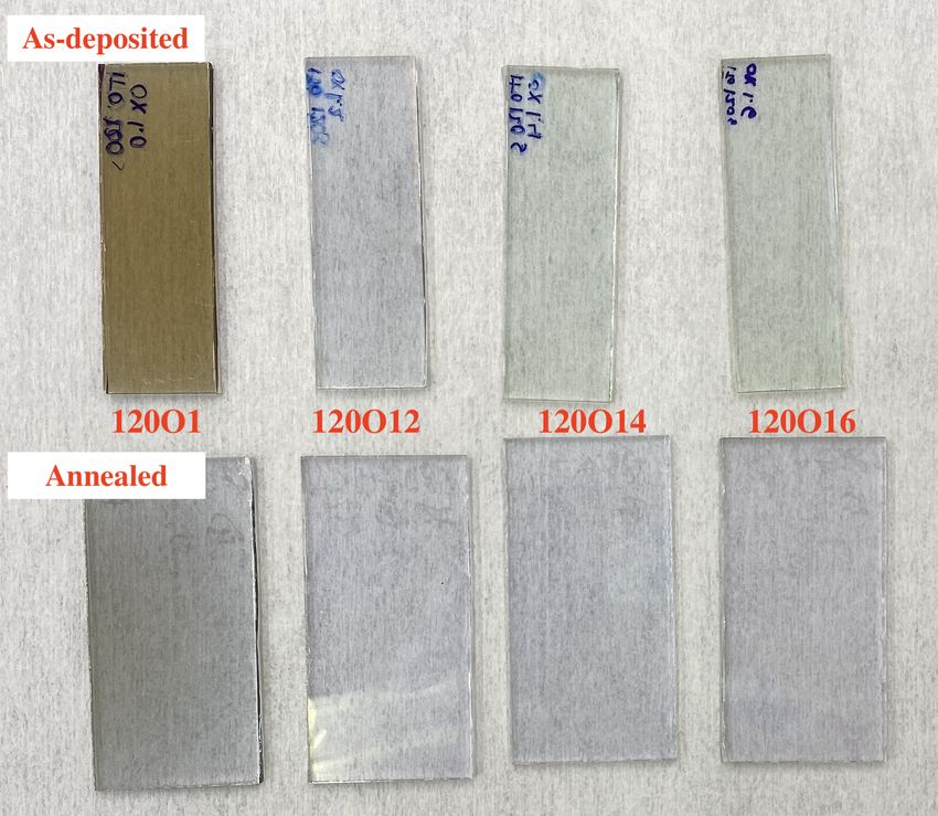
Since the samples with AZO in the bottom did not differ much from pure ITO
samples, only the latter are presented in this section. Complete raw data (sheet
resistances and absorption) can be found in Appendix C. The sheet resistance as
a function of oxygen flow is also presented in Figure 20. For deposition time 120 s,
the sheet resistance as-deposited ITO agreed with Axelsson’s thesis work [18]. In
Figure 20, local minimas for 120 and 200s can be seen around 1.2 sccm oxygen flow,
but the minima for 400s deposition time is not yet reached. The absorption in the
infrared range showed the opposite behaviour where lower oxygen flows gave large
absorption in the infrared and higher flows lower absorption. This is ascribed to
a plasmon peak shift due to different charge carrier concentrations. The amount
of charge carriers did as predicted put a trade off between high conductivity and
low absorption. The thickness of the samples were approximately 260 nm for 120 s
deposition, 430 nm for 200 s and 830 nm for 400 s. A doubling of film thickness did
not give a halving of sheet resistance which indicates that the process is non-linear.
Figure 20: Sheet resistance for ITO samples with different deposition times and
oxygen flows before and after annealing in 500 ◦C with selenium vapour (Ann).
Lines connect samples with the same deposition time.
295.1 Effect of Annealing
The annealing had great effect on the opto-electrical properties. Figure 20 clearly
shows how the large difference in sheet resistance right after sputtering diminishes
with annealing. In addition, a halving of film thickness gave an expected doubling
of sheet resistance. The drastic increased conductivity for all samples may be due
to formation of larger crystals so that electron scattering against crystal bound-
aries is lowered. Another possible explanation is higher doping concentrations by
activation of tin or removal of oxygen.
When analyzing absorption spectra before and after annealing, as the one in Fig-
ure 21, a plasmon peak shift towards shorter wavelengths is clear as a result of
annealing. This indicates that the doping concentration has increased. Figure 21
only shows data for sample 200O1 and 200O2, but the same undesired increase
of absorption in the infrared was seen for all samples produced with oxygen flow
1, 1.6 and 2 sccm (see Appendix C). On the contrary, the absorption decreased
for 1.2 sccm oxygen flow samples and no shift in the peak’s position could be de-
termined (but it lies outside the investigated wavelength region). Sample 400O14
showed a large increased absorption while 200O14 increased less significantly and
the absorption lowered when 120O14 was annealed. Decreasing intensity of the
plasmon peak but constant peak position is associated with large relaxation times,
i.e. high mobility, and constant carrier concentrations.
Ellipsometry measurements of the annealed 120O1 sample confirmed that the peak
in the infrared indeed is a plasmon peak, as 1 = 0 around 1150 nm, consistent
with the peak’s position in Figure 22a. The calculated values from the oscillator
model are presented in Figure 22b. From the model, a sheet resistance could also
be obtained and this value agreed well with the measured value. Even though
other samples’ peaks lie outside the investigated spectrum, their tails are visible
as absorption in the infrared region.
The quickly decreased absorption just before 300 nm is attributed to the glass
substrate and in reality, the ITO absorption increases towards 100% as the optical
band gap is overcomed. ITO’s band gap absorption shifted to shorter wavelengths
for all samples, indicating that the band gap widened. This is probably due to
an increased Moss-Burnstein shift as explained in section 2.1, which indicates that
the annealing led to increased carrier concentration.
30You can also read