GEFES STUDENT RESEARCH REPORT - LA0.7SR0.3MNO3/BATIO3/ITO FERROELECTRIC TUNNEL
←
→
Page content transcription
If your browser does not render page correctly, please read the page content below
GEFES Student Research Report
      La0.7Sr0.3MnO3/BaTiO3/ITO Ferroelectric Tunnel
                        Junctions

                                  Isabel Tenreiro
                               Tutor: Alberto Rivera
            GFMC, Universidad Complutense de Madrid, 28040 Madrid, Spain

                                         31 March 2021

1     Introduction
1.1    Ferroelectric tunnel junctions and memristors
    A ferroelectric tunnel junction (FTJ) is a three-layer heterostructure consisting of an ultrathin
insulating ferroelectric (FE) layer sandwiched between two conducting electrodes. In this
two-terminal device, the electron tunneling through the FE barrier is strongly coupled to its
ferroelectric polarization, which can be switched from the upward (towards the top electrode)
to the downwards (towards the bottom electrode) state by an applied electric field, giving rise
to different electro resistance states. This phenomenon is called the tunneling electroresistance
(TER) effect and provides a non-volatile memory device with nondestructive readout.

    The physical principle behind the TER effect in FTJs is the modulation of the electrostatic
potential profile of the FE barrier. The resistive switching (RS) associated to the change of
the barrier profile is usually explained in terms of the ferroelectric polarization reversal and the
different screening lengths of the electrodes [1]. Polarization surface bound-charges are induced
when the FE barrier is put in direct contact with a conducting electrode therefore, screening
charges appear in order to neutralize them and modify the electrostatic potential profile. When
the barrier is sandwiched between two different electrodes, the difference in their screening
lengths together with the dependence of the bound-charges with the polarization sense in the
FE layer cause an asymmetry in the potential profile under polarization orientation reversal,
leading to two different resistance states in electronic transport and the TER effect.

    Although the polarization reversal is one of the main factors in explaining the TER effect,
other factors, such as interface or strain effects and migration of oxygen vacancies, can also
affect or introduce an additional mechanism for the RS. This is the case of our samples based
on La0.7 Sr0.3 MnO3 /BaTiO3 (LSMO/BTO) heterostructures, as shown in the reference [2] with
top electrode of Ag, where a polarization inversion causes one RS loop, and the oxygen vacancy
migration with the polarization pointing up another one. The RS due to activated oxygen
vacancies migration is characterized by a high resistance state when the electric field is pointing
from the top electrode of Ag to the LSMO, due to the build up of a Schottky barrier at the
LSMO/BTO interface [2]. When a negative electric field (down) is applied, oxygen vacancies
are activated and driven towards the LSMO/BTO interface, n-type doping the BTO locally,
building up the Schottky barrier and increasing the resistance (Figure 1 a)). Conversely, a
positive electric field (up) removes the Schottky barrier by redistributing the oxygen vacancies
through the BTO layer electron doping it and lowering the resistance of the FTJ (Figure 1 b)).
The formation of the Schottky barrier is enhanced when the polarization is pointing towards

GFMC. UCM GEFES Research Report                                                                    1
the top electrode [2] because the depolarization field increases the energy barrier in the bottom
interface LSMO/BTO and decreases the one in the top interface BTO/Ag. This RS due to
oxygen vacancies migration can be controlled by gradually changing the voltage bias applied,
enabling access to a continuum of resistance states [2]. The access to a continuum of resistance
states turns the FTJ in what is called a tunnel memristor, which is a promising building block
for future storage devices and neuromorphic computing.
Figure 1: Energy band modulation for oxygen vacancies migration. Schematic band diagram of the FTJ with
polarization in the up state for the a) RHigh and b) RLow states. Dashed lines represent indicative energy band in absence
of polarization and applied electric field. a) Drifting of oxygen vacancies (open green circles) towards the LSMO/BTO
interface under negative electric field build up a Schottky barrier enhanced thanks to the up polarization (as compared
to the dashed line). b) The Schottky barrier at the LSMO/BTO interface is suppressed when a positive electric field is
applied, providing a RLow state.
1.2 Optical sensing of the resistive state
The FE photovoltaic (PV) effect has been widely studied for applications in several fields
as solar cells or information storage. When the thickness of the FE layer is decreased to the
nanoscale and put in direct contact with a semiconducting electrode, the bulk PV effect is
surpassed by a PV effect originated from the interfacial Schottky barrier, enhancing the light
absorption. The thinning of FE layers forming Schottky barriers with metallic electrodes is a
promising research avenue to the new generation of solar cells [3].
The aim of this work is to use the enhanced optical response of the Schottky barrier
building up in the LSMO/BTO interface, by growing a top transparent In2 O3 : SnO2 , (90 : 10)
(ITO) electrode, to get the optical sensing of the resistive state from the barrier layer in
LSMO/BTO/ITO FTJ. The use of transparent ITO as top electrode grants direct optical
access to the FTJ area. At the same time, it serves as an oxygen vacancies reservoir enhancing
the migration of vacancies and the suppression or formation of the Schottky barrier at the
LSMO/BTO interface. A different address based on the PV response of the active bottom
electrode for RS with FE switching prevalence has already proved the viability of the optical
sensing of the resistive state in FTJs [4].
2 Experimental methods
FTJs fabrication process consisted of epitaxial deposition of 20 nm of LSMO and 5 nm
of BTO onto (100) SrTiO3 (STO) substrates by high pure oxygen pressure (3.2 mbar) RF
sputtering. Tunnel junctions were fabricated by UV photolithography defining different contact
areas of 9 × 18 µm2 on positive photoresist. A 150 ± 10 nm ITO top electrode was deposited
GFMC. UCM GEFES Research Report 2through an aluminum shadow mask with DC magnetron sputtering at room temperature in a
6.3·10−3 mbar atmosphere, with a ratio in the gas chamber of 50 sccm Ar : 1 sccm O2 .
Transport characterization was performed in a closed cycle He cryostat with a Keithley
2450 sourcemeter. A two point configuration between the LSMO bottom electrode and the top
grounded ITO electrode was used, as sketched in Figure 2 a) inset.
The transparent ITO electrode enables optical access to the BTO layer of the FTJ. The device
was illuminated employing two different light sources to get information about the optically
active layer: an Oxxius UV LBX-375 nm (3.3 eV) laser diode with a spot size of 0.7 mm and a
variable power supply up to 70 mW, and a red 2 W LED by Thorlabs model M660L4 with 1.9
eV energy.
3 Results
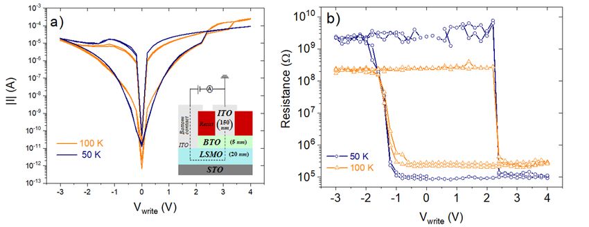
FTJs of LSMO(20 nm)/BTO(5 nm)/ITO(150 nm) were investigated. Measurement of the
electric current as a function of the applied writing voltage (Vwrite ) exhibited reproducible
pinched hysteresis loops proving the existence of resistive switching in the FTJ. Figure 2 a)
portrays two consecutive |I|−V curves at 50 K and 100 K where the negligible differences between
them confirm the good stability of both resistive states. Figure 2 b) shows the corresponding
two consecutive electroresistance switching loops at the same temperatures as in Figure 2 a),
in which the resistance state is set with a writing voltage (Vwrite ) and the differential resistance
is read with a lower reading voltage (Vread ) of 100 mV; small enough not to switch the state.
The RS loops manifest that positive voltages over 2.4 V settle the low resistance state (RLow )
or ON state, where it remains stable until negative voltages under -1.6 V switch back the high
resistance state (RHigh ) or OFF state. These results indicate that the resistive switching is
ruled by a Schottky barrier modulation due to oxygen vacancies migration, and are opposite
to the ones expected when the RS is arising from pure FE polarization inversion [2],[5], where
the RHigh state is observed when applying positive Vwrite , and the RLow state for negative Vwrite .
Figure 2: a)“Pinched” two consecutive |I|-V loops at 50 K and 100 K. Inset depicts a sketch of the structure and
electrical configuration on the FTJ. b) Resistive switching loops at 50 and 100 K read with 0.1 V.
A negative electric field drives oxygen vacancies to the LSMO/BTO interface, accumulating
them, generating the Schottky barrier and increasing the resistance, yielding the RHigh state.
Conversely, an applied positive electric field promotes the diffusion of oxygen vacancies from the
LSMO/BTO interface to the BTO layer and/or the ITO electrode (Figure 1 a), b)). This turns
GFMC. UCM GEFES Research Report 3the BTO into a metallic layer, suppresses the Schottky barrier in the LSMO/BTO interface and
sets the RLow state. Note that the increase of the RHigh resistance when the temperature is
reduced (Figure 2 b)) supports the thermionic injection transport mechanism over a Schottky
barrier. RHigh /RLow over 105 are achieved at low temperatures showing highly competitive ratios
of special relevance for memory-based devices.
Current versus voltage (I-V) curves in dark
and under UV illumination were performed
to investigate the PV response of the FTJs.
While I-V curves for the RLow state do not
present any photovoltaic effect (i.e. for I=0,
V=0), I-V curves in the RHigh state evidence
a measurable photovoltaic response under
UV illumination, an open circuit voltage
Voc (voltage at zero current) and a short
circuit current Isc (current at zero voltage) are
observed [6]. Figure 3 shows the I-V curves
at 14 K, in the RHigh state, when illuminating
the junction with a 375 nm laser (3.3 eV), at
different light power densities. Significant Isc
Figure 3: PV response on the RHigh state. I-V
curves at 14 K in the RHigh state under UV (3.3 eV) laser and Voc are evidenced above power densities
illumination for varying power densities. Dark I-V before and over 1 W/cm2 , but suggestions of photo
after UV illumination and under red LED illumination (1.9
eV at 0.3 W/cm2 ) are shown for comparison.
response are already present in I-V curves
at lower power densities of 0.2 W/cm2 at
negative voltages as they differ from the I-V
curve measured in dark, represented by the black solid curve. Comparison between dark I-V
curves before and after UV illumination shows no appreciable differences evidencing no damage
is done to the FTJ during the laser illumination.
Increase of Isc with UV light power density
points out illumination as the origin of PV
effect. No PV effect is observed when
illuminating the junctions with a red LED
(1.9 eV) with an estimated power density
of 0.28 W/cm2 . This fact together with
the disappearance of the PV effect when
switching to RLow evidences the excitation
of charge carriers is generated in the BTO
layer, which has a wide bandgap of 3.2 eV.
Generation of photo-excited carriers occurs
under illumination with UV light above the
optical bandgap of the active layer, the
BTO, (Figure 4). Photocarriers are then Figure 4: Photovoltaic effect originated from the
separated by the built-in electric field (Ebi ) interfacial Schottky barrier. Schematic band diagram of
the RHigh state. Generation of electron – hole pairs (solid
that arises in the depletion region of the – open circles) under UV-illumination and separation of the
Schottky barrier, a process facilitated by photogenerated charges by the Ebi in the depletion width
(WF ) originating a reversed bias photocurrent.
the polarization pointing towards the ITO
electrode (Figure 4). The photocurrent is in
the opposite sense to the FE polarization, i.e. an inversely biased current of a Schottky-based
PV effect Figure 4 [3],[6]. Therefore, a PV response is observed in the RHigh state of the FTJ,
while the suppression of the Schottky barrier removes the PV response in the RLow state. The
GFMC. UCM GEFES Research Report 4different optical behavior of the RLow and RHigh states due to the suppression and build-up of
a Schottky barrier-PV effect enables the optical sensing of the resistive state of the FTJ.
4 Conclusions
In this project, the optoelectronic response of LSMO(20 nm)/BTO(5 nm)/ITO(150 nm)
FTJs were investigated. Electroresistive switching was confirmed to be originated by the
suppression and formation of a Schottky barrier at the LSMO/BTO interface due to oxygen
vacancies migration, obtaining RHigh /RLow ratios up to 105 at 50 K. The top ITO electrode
incorporates the light functionality of the device, showing a solid PV response in the RHigh state
under UV illumination, which is removed switching the FTJ to the RLow state. The origin of
the PV effect is the Schottky barrier generated at the LSMO/BTO interface with the RS, which
enables a fast and active optical readout of FTJs high resistive state, opening a new route for
the optical sensing of FTJ memories and memristors towards room temperature.
References
[1] Rui Guo et al. “Ferroic tunnel junctions and their application in neuromorphic networks”.
In: Applied Physics Reviews 7.1 (Mar. 2020), p. 011304.
[2] D. Hernandez-Martin et al. “Controlled Sign Reversal of Electroresistance in Oxide Tunnel
Junctions by Electrochemical-Ferroelectric Coupling”. In: Physical Review Letters 125.26
(Dec. 2020), p. 266802.
[3] Zhengwei Tan et al. “Thinning ferroelectric films for high-efficiency photovoltaics based on
the Schottky barrier effect”. In: NPG Asia Materials 11.1 (Dec. 2019), pp. 1–13.
[4] Wei Jin Hu et al. “Optically controlled electroresistance and electrically controlled
photovoltage in ferroelectric tunnel junctions”. In: Nature Communications 7.1 (Feb. 2016),
pp. 23955–6900.
[5] M. Ye Zhuravlev et al. Erratum: Giant electroresistance in ferroelectric tunnel junctions
(Physical Review Letters (2005) 94 (246802)). Apr. 2009.
[6] A. Rivera-Calzada et al. “Switchable Optically Active Schottky Barrier in
La0.7Sr0.3MnO3/ BaTiO3/ITO Ferroelectric Tunnel Junction”. In: Submitted to Advanced
Electronic Materials (Submitted 2021).
GFMC. UCM GEFES Research Report 5You can also read