Asymmetric Spacer Junctionless GAA Nanowire FET for Continued Scaling
←
→
Page content transcription
If your browser does not render page correctly, please read the page content below
Asymmetric Spacer Junctionless GAA Nanowire FET for Continued Scaling Bharath Sreenivasulu Vakkalakula ( vbharathsree818@gmail.com ) National Institute of Technology Warangal https://orcid.org/0000-0003-3064-1522 Narendar Vadthiya National Institute of Technology Warangal Research Article Keywords: Nanowire FET, Junctionless, Scaling, Asymmetric spacer, Analog/RF, Quantum effects. Posted Date: August 30th, 2021 DOI: https://doi.org/10.21203/rs.3.rs-852428/v1 License: This work is licensed under a Creative Commons Attribution 4.0 International License. Read Full License
Asymmetric Spacer Junctionless GAA Nanowire FET for

 Continued Scaling
 V. Bharath Sreenivasulu1 and Vadthiya Narendar2

 1, 2
 Department of Electronics & communication Engineering

 National Institute of Technology Warangal, Warangal-506004, Telangana, India

 E-mail: vbharathsree818@gmail.com and narendarv@nitw.ac.in
Abstract:

We demonstrate junctionless (JL) n-channel SOI nanowire FET with asymmetric spacer at nano regime.

The impact of various spacer dielectrics on device performance is presented and various electrical

characteristics are analyzed. The gate length (LG) scaling impact of the asymmetric spacer with various

spacers on ION, IOFF, and ION/IOFF is analyzed. The device exhibits excellent electrical characteristics with

SS = 64 mV/dec, DIBL = 45 mV/V, ION/IOFF = 106 even at 5 nm LG ensures better electrostatic integrity.

From the result analysis it is noted that spacer plays a detrimental role in reducing OFF current (IOFF) at

lower LG. Moreover, the power analysis on scaling with various spacer dielectrics is performed. The

analog/RF performance is also performed and scaling feasibility with HfO2 spacer is presented. The result

analysis ensures asymmetric JL nanowire FET is one of the possible options to continue scaling.

Keywords: Nanowire FET, Junctionless, Scaling, Asymmetric spacer, Analog/RF, Quantum effects.
1 Introduction:

 The use of stacked nanowire field-effect transistors (NW-FETs) as a scaling alternative for CMOS

 technology has been proposed [1]. The Gate-All-Around construction provides minimal OFF-current (IOFF)

 and a sharp subthreshold slope, while multiple wires stacking results in high drive current (ID) with a

 footprint equivalent to FinFET [2]. By arranging transistors and selectors vertically, vertical NW-FETs have

 the potential to greatly enhance device density [3]. Stacking nanowires present a number of technical

 obstacles. The manufacturing of inner spacers, in particular, has been identified as a possible stumbling

 point for the technology. To decrease parasitic capacitances, these spacers divide the gate stack between the

 nanowires and the highly doped source/drain regions. In critical VLSI system manufacturing [4], NW-FETs

 could be made in high yield, and nanosheet and NW thickness can be scaled down to sub-10 nm [5]. So that

 even with the most aggressive node scaling, the electrical characteristics may be maintained. Inner spacers

 are now being used in NW-FETs, according to recent research [6]. Moreover, in recent times much attention

 is kept on junctionless (JL) FETs to continue scaling for the sub-10 nm domain. Compared to conventional

 inversion mode FETs the JL FETs have the following advantages: (a) It alleviates the thermal budget

 constraint imposed by the absence of source/drain junctions. (b) Because lateral diffused drain, pocket

 implantation, and shallow junction are no longer required, the manufacturing flow is simplified. (c) Because

 the major conducting path is through the highly doped silicon bulk, the interface between the oxide and the

 semiconductor channel has high immunity to surface scattering [7-9].

The need for a spacer between source and drain terminals is fundamental for sub-10 nm technology nodes to

overcome SCEs. However, the introduction of spacer raises the series resistance between potentials terminals

resulting in increased ION. Hence to achieve high performance of a device spacer dielectrics are introduced

which boosts ION and improves subthreshold performance. Moreover, to boost DC, analog/RF metrics i.e.,

for mixed signal design applications the asymmetric spacer is studied. The introduction of asymmetric spacer

leads to the reduction of IOFF by 57% [10]. Moreover, the asymmetric spacer also reduces direct tunneling

between channel and drain and also reduces the feedback miller capacitance effect. By adding extra

photolithographic process phases to current technologies asymmetrical devices are developed. Additional
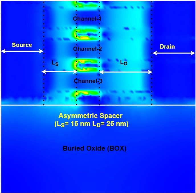
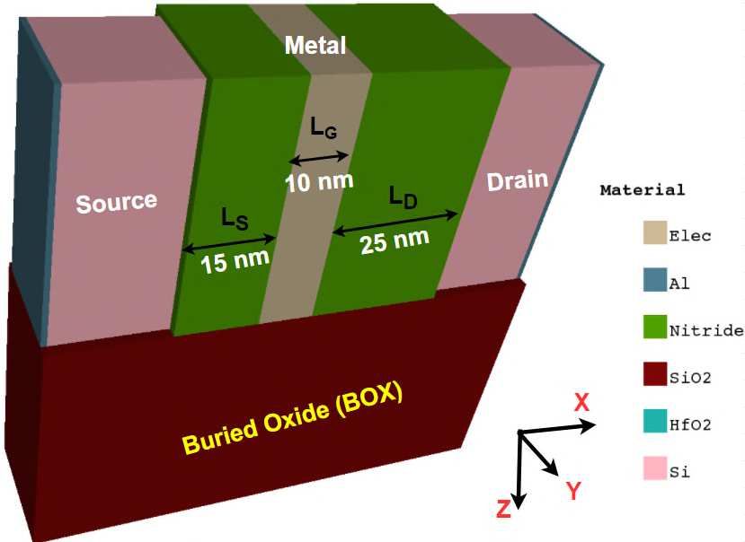
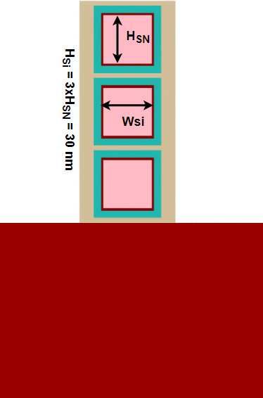
photolithographic techniques need more photomasks and exposure equipment, as well as more time in the

manufacturing process, raising costs and lowering yield. On the other hand, Cheng et al., developed a method

for producing asymmetrical structures that do not require photolithographic steps, thus saving time and

money [11].

The following is an analysis of the paper's content. The paper's technique and important technological

characteristics are described in Section 2. Section 3 discusses the effects of electrical performance on an

asymmetric spacer. Section 4 explains how LG scaling affects electrical properties.

2. Device structure and simulation details:

 (a) (b)

 Fig. 1. 3-D channel SOI JL nanowire FET (b) 2-D cross section view at center of fin.

 The 3D and 2D schematic view of junctionless (JL) nanowire FET is depicted in Fig.1. The nanosheet FET

 with gate length, width, and height of 10 nm is considered. The source and drain pad lengths are 20 nm. The

 SiO2 with 0.5 nm is considered as interfacial oxide and HfO2 is 3 nm with EOT of 0.75 nm is maintained.

 The doping for the whole Si bar is 1 × 1019 cm-3 is considered. The gate metal work function of 4.8 eV is

 maintained. The source side fin extension of 15 and drain side fin extension of 25 nm are maintained to form

 an optimized asymmetric spacer. The contact resistivity of 1 × 10⁻⁹ Ω.cm2 is considered. he buried oxide is

 maintained with SiO2 material. The spacer is maintained with Air, SiO2, Si3N4, and HfO2 dielectric materials.

 Drift–diffusion model was used to simulate the proposed devices, and the following equations were produced

 by solving the drift–diffusion model, current density expressions, and Poisson equation. These are referred
to as

 . ɛ Ψ = − ( − + = + + + ) (1)

 The electron and hole concentrations are denoted by and , respectively, Ψ is the electrostatic potential of

 the vacuum level, the ionized doping concentrations are given by + and + , and the electron charge is

 given by q. The temperature of the lattice should be consistent throughout the Drift–diffusion scenario.

 1 1 1 1
 = + + (2)
 µ µ µ µ

 To accommodate for doping dependent mobility (mobility deterioration owing to surface rough scattering)

 and acoustic phonon in silicon lattice, the Lombardi unified mobility model was utilized.

 Shockley–Read–Hall (SRH), Auger, and direct recombination were all taken into account using the Carrier

 recombination model. As a result, final recombination U is equal to

 = + + (3)

The electron and hole quantum correction equation can be written as:

 ℎ2 2 √
ᴧn = − (4)
 6 √

 ℎ2 2 √
ᴧp = (5)
 6 √
Figure 2. The calibrated ID-VGS simulation [12].

The TCAD parameters were well calibrated by fitting the ID-VGS of the 10-nm node FinFETs, as illustrated in

Fig. 2.

3. Result analysis

 On scaling, the comparison of ION, IOFF, ION/IOFF, SS, and DIBL characteristics is examined. Scaling LG from

 20 nm to 5 nm illustrates, spacer materials influence ID-VGS features. The device obtains decreased IOFF with

 HfO2 spacer approaching less than pA range at LG of 5 nm, as shown in Fig. 3(a), ensuring further scaling.

 The decrease in IOFF as the ‘k' value increases is because of the increased electric field in the OFF state. The

 ID, on the other hand, is unaffected by the flat band condition in the ON state, which results in zero electric

 field. The JL technology enters accumulation mode after a flat band state, and the spacer somewhat improves

 ID. Because of increased series resistance and the lack of spacer fringing fields, the device suffers from a

 greater IOFF when no spacer material is present. As a result, at ultra-scaled LG, spacer dielectric plays a vital

 role in deciding performance in order to avoid leakages and mitigate SCEs. Except for Air and no spacer

 dielectric, the device has an IOFF of less than nA for all dielectric spacer combinations at LG = 5 nm. Figure

 3(b) shows the same pattern in ID-VGS, with a 4-order improvement in IOFF as spacer dielectrics are changed.

 Figure 3(c) and 3(d) show a less than 2 order improvement in IOFF with spacer dielectrics at 14 nm and 20

 nm LG compared to other LG due to reduced fringing effects. Because the presence of more LG increases gate

 electrostatic integrity, IOFF is effectively reduced. Furthermore, because of the increased doping in the JL fin

 extension, the gate fringing fields are unaffected by changes in resistance at higher gate bias, producing in

 minor variations in ION and IOFF.
(a) (b)

 (c)

 (d) (e)

Figure. 3 Asymmetric spacer scaling at (a) LG = 5 nm (b) LG = 7 nm (c) LG = 10 nm (d) LG = 14 nm (e) LG =

20 nm.
(a) (b)

Figure. 4 Asymmetric spacer variations on (a) ON current (ION) (b) threshold voltage (Vth)

Figure 4(a) depicts the ION variation with various spacer dielectrics from 20 nm to 5 LG. From results it is

noticed that highest ION is obtained at 5 nm LG with HfO2 spacer and lowest with no spacer at 20 nm. For a

device highest ION represents high performance. Figure 4(b) depicts the LG variation for various spacer

dielectrics. The device attains highest Vth with HfO2 spacer at 20 nm LG, and lowest with no spacer dielectric

at 5 nm LG. Higher Vth ensures better subthreshold performance.

 (a)
(b)
Figure. 5 Asymmetric spacer dielectric variation on (a) OFF current (IOFF) (b) ION/IOFF ratio.

Figure 5(a) depicts the IOFF of asymmetric nanowire FET with various spacers. The device exhibits lowest IOFF

at LG = 20 nm with HfO2 spacer. Moreover, the device exhibits highest IOFF with no spacer at LG = 5 nm.

However, with SiO2, Si3N4, HfO2 spacers the device exhibits IOFF lesser than nA which is feasible for scaling

towards low power applications. Figure 5(b) depicts the ION/IOFF of asymmetric nanowire FET with various

spacers. The device exhibits highest ION/IOFF with HfO2 spacer at 20 LG. Moreover, the device shows lowest

ratio at 5 nm with no spacer dielectric. The device exhibits ION/IOFF ratio greater than 106 with Si3N4 and HfO2

spacers.

 (a)
(b)

Figure. 6 Asymmetric spacer dielectric variation on (a) DIBL (b) SS.

The mathematical form of SS and DIBL is given as follows [13, 14]:

 ( − )
DIBL (mV/V) = |( th1 − th2 )| (1)
 DS1 DS2

 log10 ( D ) −1
SS (mV/dec) = [ ] (2)
 GS

Figure 6(a) depicts the DIBL performance with scaling from 20 nm down to 5 nm with various spacers. The

device exhibits highest DIBL at 5 nm with no spacer dielectric and lowest DIBL with HfO2 spacer at 20 nm

LG. Larger value of spacer dielectric reduces DIBL impact due to series connected capacitance. The SS impact

of dielectric spacer on nanowire FET from 20 nm to 5 nm LG is depicted in Fig 6(b).
(a)

 (b)

Figure. 7 Asymmetric spacer variations on (a) Electric field (b) Potential with HfO2 spacer.

Figure 7 depicts the electric field and potential distribution of asymmetric spacer nanowire FET in ON state

i.e., VDS = 0.9 V and VGS = 1.2 V. In Fig 7(a), Due to large spacer distance between channel and drain, there

is less impact of electric field distribution on channel and thus reduces hot carriers and impact ionization.

Moreover, in Fig 7(b), the large spacer distance even with high-k spacer reduces potential distribution over

channel region.

4. Scaling effect of nanosheet FET

 Figure 8(a) depicts the first derivative (gm ) of the transfer characteristics at VDS of 0.9 V. The

 transconductance (gm ) is an important analog metric detrimental in obtaining better gain, amplification and

 cut-off frequencies [15]. The device exhibits maximum peak of gm with 0.119 mS at LG = 20 nm at 1 V and

 gm with 0.125 mS at LG = 5 nm. The peaks of gm have a window for VGS values between 0.85 and 1 V ensuring

 potential for low power and high-speed operating capability.
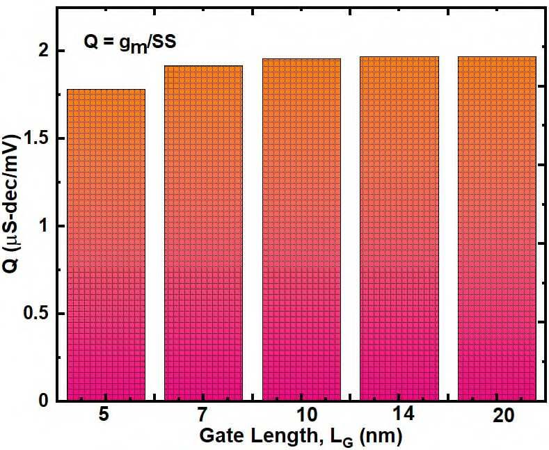
(b) (c)

 Fig. 8. Asymmetric spacer impact with gate length (LG) variation on (a) Transconductance (gm ) (b)

 Transconductance generation factor (TGF).

 Figure 8(b) depicts the transconductance generation factor (TGF) with LG variation from 5 nm to 20 nm. The

 TGF is an important metric in determining the power required to obtain high speed with respect to gate bias.

 The TGF determined how current can be used to achieve a desired gm value [16]. Due to the exponential

 dependence of ID on VGS in the subthreshold zone, the TGF is constant and high, but it diminishes at high VGS

 because of mobility deterioration. From the Fig 8(b) it is observed that TGF is more at LG = 20 nm and lower

 at LG = 5 nm.

Fig. 9. Asymmetric spacer impact with gate length (LG) variation on (a) Threshold voltage (Vth) (b) Q.
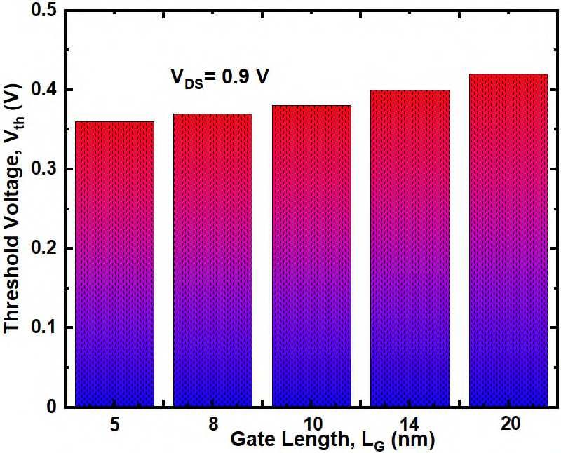
Figure 9(a) depicts the Vth variation with LG scaling at VDS = 0.9 V. Increase in LG value enhances Vth due to

improved gate control over channel. Narrow channel enhances Vth value and thus have better gate

electrostatics. The device exhibits Vth of 0.4 V at LG= 20 nm and 0.35 V at LG = 5 nm. Even for lower scaled

dimensions the device exhibits better Vth which is reasonable for driving logic device applications. Figure 9(b)

depicts the variation of SS with various LG at VDS = 0.9 V. it is observed that increase in LG SS decreases due

to reduction of drain influence on channel. Moreover, at scaled LG of 5 nm the device exhibits SS of 65 which

stays below thermal limit of 80 mV/dec and thus ensure device drivability for low power applications.

Fig. 10. Asymmetric spacer impact with gate length (LG) variation on (a) gg and gd (b) gs and ox .
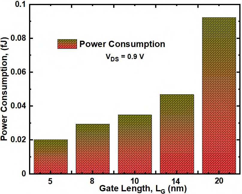
Figure 10(a) depicts the effect of gd and gg on LG variation with respect to VGS at VDS = 0.7 V. Increases in

LG the total capacitance and miller capacitance increases [17]. The device exhibits gd of 0.9 fF at LG = 20 nm

and at LG = 5 nm it shows 0.2 fF which is 4x times reduction. Reduced gd with scaling ensures reduced power

consumption and better transient response.

Figure 10(b) depicts the effect of gs and ox on LG variation with respect to VGS at VDS = 0.7 V. The parasitic

capacitance gs and intrinsic capacitance ox decreases with LG scaling [18]. The device exhibits gs of 0.2

fF at LG = 5 nm and 0.1 fF which is 5x times increment. ox is the oxide capacitance which is detrimental in

calculation of power consumption and dynamic power.

 (a) (b)

Fig. 11. Asymmetric spacer impact with gate length (LG) variation on (a) Dynamic Power (b) Power

Consumption.

The dynamic power is the power consumption due to charge and discharging cycles. The mathematical

expression for dynamic power is (COX VDD 2 ) [19, 20] and is depicted in Fig. 11(a). The device shows DP of

0.01 at LG = 5 nm and 0.05 at LG = 20 nm which is 4x times more. Thus, scaling results decrease in dynamic

power and ensures device feasibility for low power applications. The power consumption is the power required

 1
to drive the circuit [21]. The power consumption is mathematically expressed as ( COX VDD 2 ) [22, 23] and is
 2

depicted in Fig. 11(b). The power consumption also reduces with LG scaling. At LG = 5 nm the device exhibits

0.02 fJ and at LG = 20 nm 0.9 fJ which is 4x times higher.
Fig. 12 Asymmetric spacer impact with gate length (LG) variation on (a) intrinsic delay (b) Cut-off frequency

(c) Gain bandwidth product.

The intrinsic delay (τ) value is determined at VDD value of 0.9 V and is depicted in Fig 12. For LG value of 20

nm the device exhibits τ of 3.5 ps and for 5 nm LG the device shows 0.6 ps. decrease in LG results reduced τ.

The cut-off frequency determines the speed of the circuit and can be expressed as. The device exhibits ft of

0.45 THz at LG = 5 nm and 0.08 THz at LG = 20 nm. The gain bandwidth product (GBW) is another important

figure of merit for determining overall performance of a device [16]. The device exhibits GBW of 0.09 THz

with 5 nm LG and 0.04 THz with 20 nm LG.
5. Conclusion

The dielectric impact on asymmetric spacer JL SOI nanowire FET has been studied towards scaling. The

dielectric is predominant and fundamental at lower LG compare to higher one. The device achieves better

ION, IOFF, ION/IOFF, SS and DIBL at LG = 20 nm with HfO2 spacer. However, Si3N4, HfO2 spacers exhibits

better overall performance and ensures possibility for scaling towards lower nodes. Moreover, the device

exhibits better analog/RF metrics towards scaling. Result analysis shows the asymmetric spacer outperforms

device performance for DC, analog/RF and ensures better option for scaling.

References:

 1. T. Ernst et al., ‘‘Novel 3D integration process for highly scalable nanobeam stacked-channels GAA (NBG)

 FinFETs with HfO2/TiN gate stack,’’ IEDM Tech. Dig., San Francisco, CA, USA, Dec. 2006, pp. 1–4. doi:

 10.1109/IEDM.2006.346955.

 2. S. Barraud et al., "Performance and design considerations for gate-all-around stacked-NanoWires

 FETs," 2017 IEEE International Electron Devices Meeting (IEDM), 2017, pp. 29.2.1-29.2.4, doi:

 10.1109/IEDM.2017.8268473.

 3. D. Yakimets, G. Eneman, P. Schuddinck, T. Huynh Bao, M. Garcia Bardon, P. Raghavan, A. Veloso, N.

 Collaert, A. Mercha, D. Verkest, A. V.-Y. Thean, and K. De Meyer, “Vertical GAAFETs for the ultimate

 CMOS scaling,” IEEE Trans. Electron Devices, vol. 62, no. 5, pp. 1433-1439, May 2015, doi:

 10.1109/TED.2015.2414924.

 4. W. Lu and C. M. Lieber, “Semiconductor nanowires,” J. Phys. D: Appl. Phys., vol. 39, no. 21, p. R387, Oct.

 2006. [Online]. Available: http://stacks.iop.org/0022-3727/39/i=21/a=R01

 5. Y. Wu et al., “Controlled growth and structures of molecular-scale silicon nanowires,” Nano Lett., vol. 4, no.

 3, pp. 433–436, Feb. 2004. [Online]. Available: http://dx.doi.org/10.1021/nl035162i.

 6. H. Mertens et al., ‘‘Vertically stacked gate-all-around Si nanowire transistors: Key process optimizations and

 ring oscillator demonstration,’’ IEDM Tech. Dig., San Francisco, CA, USA, Dec. 2017, pp. 37.4.1–37.4.4.

 doi: 10.1109/IEDM.2017.8268511.
7. Bharath S. V. and Narendar. V, Design and Insights into Sub-10 nm Spacer Engineered Junctionless

 FinFET for Nanoscale Applications. ECS Journal of Solid State Science and Technology 10 (1) (2021)

 013008.

8. V. B. Sreenivasulu, V. Narendar, Performance improvement of spacer engineered n-type soi finfet at

 3-nm gate length, AEU-International Journal of Electronics and Communications 137 (2021) 153803.

9. V. Bharath Sreenivasulu, Vadthiya Narendar, Characterization and optimization of junctionless gate-

 all-around vertically stacked nanowire FETs for sub-5 nm technology nodes, Microelectronics

 Journal,2021,105214, https://doi.org/10.1016/j.mejo.2021.105214.

10. A. Goel, S. K. Gupta, K. Roy, Asymmetric drain spacer extension (adse) finfets for low-power and

 robust srams, IEEE Transactions on Electron Devices 58 (2) (2010) 296–308.

11. Cheng et.al., Method of forming asymmetric spacers and methods of fabricating semiconductor device

 using asymmetric spacers, U.S. patent 0 233 691, 2008.

12. Rumar R, Kumar A (2020) Hetro-Dielctric (HD) oxide-engineered junctionless double gate all around

 (DGAA) nanotube field effect transistor (FET). Silicon

13. V. Narendar, R. Mishra, Analytical modeling and simulation of multigate finfet devices and the impact

 of high-k dielectrics on short channel effects (sces), Superlattices and Microstructures 85 (2015) 357–

 369.

14. Navaneetha A, Reddy AK, Deepthi SA, et al. Performance evaluation of noise coupling on germanium

 based TSV filled material for future IC integration technique. Mater Today Proc. 2021; 45:1494-1497.

15. C. K. Pandey, A. Singh, S. Chaudhury, A simulation-based analysis of effect of interface trap charges

 on dc and analog/HF performances of dielectric pocket SOI-Tunnel FET. Microelectronics Reliability

 122 (2021) 114166, https://doi.org/10.1016/j.microrel.2021.114166.

16. R. Saha, Simulation study on ferroelectric layer thickness dependence RF/Analog and linearity

 parameters in ferroelectric tunnel junction TFET, Microelectronics Journal, 113 (2021) 105081.

17. N. Gupta, A. Kumar, Assessment of High-k Gate Stack on Sub-10 nm SOI-FinFET for High

 Performance Analog and RF Applications Perspective ECS J. Solid state Sci. Technol.9 123009 2020.
18. Roy Barman, Kuheli Baishya, Srimanta 2019, An insight to the performance of vertical super-thin body (VSTB) FET in presence of interface traps and corresponding noise and RF characteristics, Applied Physics A, 125, 865, 2019. 19. Chahardah Cherik, Iman Mohammadi, Saeed2021 Germanium-source L-shaped TFET with dual in- line tunneling junction Applied Physics A 127, 525. 20. Yu E, Lee W, Jung J, Cho S. Ultrathin SiGe shell channel p-type FinFET on bulk Si for sub-10-nm technology nodes. IEEE Transac Electron Dev. 2018; 65: 1290-1297. 21. A.K. Panigrahy, Ghosh, T., Vanjari, S.R.K. and Singh, S.G., 2019. Surface density gradient engineering precedes enhanced diffusion; drives CMOS in-line process flow compatible Cu–Cu thermocompression bonding at 75° C. IEEE Transactions on Device and Materials Reliability, 19(4), pp.791-795. 22. V. B. Sreenivasulu, V. Narendar, Design and temperature assessment of junctionless nanosheet fet for nanoscale applications, Silicon (2021) 1–12. https://doi.org/10.1007/s12633-021-01145-w. 23. Sreenivasulu, V. B., Narendar, V. A Comprehensive Analysis of Junctionless Tri-gate (TG) FinFET Towards Low-power and High-frequency Applications at 5-nm Gate Length. Silicon (2021). Author Contributions V. Bharath Sreenivasulu: Writing- Original draft preparation, Formal Analysis, Investigation, Simulation, Data Curation. V. Narendar: Supervision, Resources. Financial interests: The authors declare they have no financial interests. Funding: No Funding Received. Conflict of Interest: The author has no conflicts of interest to declare that are relevant to the content of this article. Compliance with Ethical Standards: The contents of this manuscript are not now under consideration for publication elsewhere; The contents of this manuscript have not been copyrighted or published previously The contents of this manuscript will not be copyrighted, submitted, or published elsewhere, while acceptance by the Journal is under consideration. Availability of data and material: Not applicable. Consent to Participate: Not applicable. Consent for Publication: Not applicable.
Acknowledgements: The authors thank to the department of Electronics and Communications Engineering,
NIT Warangal for providing the TCAD Tools.
You can also read