Feasibility Study of a Time-of-Flight Brain Positron Emission Tomography Employing Individual Channel Readout Electronics

Page created by Victor Collins
 
CONTINUE READING
Feasibility Study of a Time-of-Flight Brain Positron Emission Tomography Employing Individual Channel Readout Electronics
sensors
Article
Feasibility Study of a Time-of-Flight Brain Positron Emission
Tomography Employing Individual Channel Readout Electronics
Kuntai Park            , Jiwoong Jung * , Yong Choi * , Hyuntae Leem and Yeonkyeong Kim

                                          Molecular Imaging Research & Education (MiRe) Laboratory, Department of Electronic Engineering,
                                          Sogang University, Seoul 04107, Korea; hj11113@gmail.com (K.P.); lht0898@gmail.com (H.L.);
                                          dusrud026@gmail.com (Y.K.)
                                          * Correspondence: aegis0223@gmail.com (J.J.); ychoi@sogang.ac.kr (Y.C.)

                                          Abstract: The purpose of this study was to investigate the feasibility of a time-of-flight (TOF) brain
                                          positron emission tomography (PET) providing high-quality images. It consisted of 30 detector
                                          blocks arranged in a ring with a diameter of 257 mm and an axial field of view of 52.2 mm. Each
                                          detector block was composed of two detector modules and two application-specific integrated circuit
                                          (ASIC) chips. The detector module was composed of an 8 × 8 array of 3 × 3 mm2 multi-pixel
                                          photon counters and an 8 × 8 array of 3.11 × 3.11 × 15 mm3 lutetium yttrium oxyorthosilicate
                                          scintillators. The 64-channel individual readout ASIC was used to acquire the position, energy, and
                                          time information of a detected gamma ray. A coincidence timing resolution of 187 ps full width at
                                          half maximum (FWHM) was achieved using a pair of channels of two detector modules. The energy
                                          resolution and spatial resolution were 6.6 ± 0.6% FWHM (without energy nonlinearity correction)
                                and 2.5 mm FWHM, respectively. The results of this study demonstrate that the developed TOF brain
         
                                          PET could provide excellent performance, allowing for a reduction in radiation dose or scanning
Citation: Park, K.; Jung, J.; Choi, Y.;   time for brain imaging due to improved sensitivity and signal-to-noise ratio.
Leem, H.; Kim, Y. Feasibility Study of
a Time-of-Flight Brain Positron           Keywords: positron emission tomography (PET); brain PET; time-of-flight (TOF); application-specific
Emission Tomography Employing             integrated circuit (ASIC); TOFPET2; coincidence timing resolution (CTR)
Individual Channel Readout
Electronics. Sensors 2021, 21, 5566.
https://doi.org/10.3390/s21165566

                                          1. Introduction
Academic Editor: Arunas
Ramanavicius                                    As population aging progresses globally, the importance of early diagnosis and pe-
                                          riodic monitoring of brain diseases such as Alzheimer’s disease and Parkinson’s disease
Received: 24 July 2021                    is increasing [1–3]. Positron emission tomography (PET) is a widely used clinical and
Accepted: 15 August 2021                  research medical imaging device, which is very useful for diagnosing brain diseases as
Published: 18 August 2021                 well as various cancers and heart diseases [3,4]. However, conventional whole-body PET is
                                          not optimized for brain imaging, resulting in increased radiation dose or scanning time
Publisher’s Note: MDPI stays neutral      and compromised image quality [3,5–8]. Therefore, in order to accurately and efficiently
with regard to jurisdictional claims in   diagnose brain diseases, it is necessary to develop a dedicated brain PET with excellent
published maps and institutional affil-   system performance that provides high-quality images.
iations.                                        In order to increase the sensitivity, which depends on the geometric efficiency, the ring
                                          diameter of the dedicated brain PET needs to be reduced as much as possible. However,
                                          the reduced ring diameter of the dedicated brain PET induces the increased scatter and
                                          random coincidence counting rates (CCRs), and the decreased noise equivalent counting
Copyright: © 2021 by the authors.         rate (NECR) [3,6]. The increases in the scatter and random CCRs add a relatively uniform
Licensee MDPI, Basel, Switzerland.        background to the image, reducing contrast-to-noise ratio, signal-to-noise ratio (SNR), and
This article is an open access article    quantitative accuracy [9–11]. In particular, since the random CCR is proportional to the
distributed under the terms and           square of the single counting rate, it increases more than the true CCR and scatter CCR.
conditions of the Creative Commons        Furthermore, unlike the scatter CCR, it is proportional to the width of the coincidence
Attribution (CC BY) license (https://     timing window related to the coincidence timing resolution (CTR) [9]. Therefore, a PET
creativecommons.org/licenses/by/          detector with excellent CTR is required to decrease the random CCR.
4.0/).

Sensors 2021, 21, 5566. https://doi.org/10.3390/s21165566                                                  https://www.mdpi.com/journal/sensors
Feasibility Study of a Time-of-Flight Brain Positron Emission Tomography Employing Individual Channel Readout Electronics
Sensors 2021, 21, 5566                                                                                          2 of 15

                               Time-of-flight (TOF) PET is theoretically possible to determine the location where
                         an annihilation event occurred along the line of response (LOR) using the difference in
                         arrival times of two 511-keV gamma rays detected by a pair of detectors. The location of
                         the occurred annihilation event with respect to the midpoint between the two detectors
                         is given by ∆x = c × ∆t/2, where c is the velocity of light (3 × 1010 cm/s) and ∆t is the
                         time difference. In terms of the clinical performance of a PET, this decreases radiation dose
                         and scanning time and enables more accurate quantification. In terms of the image quality,
                         this improves SNR by reducing the background added to the image. The SNR is roughly
                         proportional to the square root of the NECR assuming that an object is a cylinder with
                         a uniform activity distribution located in the center of the field of view (FOV) and that
                         attenuation, scatter, and random corrections are perfectly applied. If TOF information is
                         incorporated into√ the analytical image reconstruction algorithm, the estimated TOF SNR
                         gain is equal to D/∆x, where D is the size of the object. That is, as the CTR proportional
                         to the error of ∆t improves, the SNR of the image improves due to an increase in the NECR
                         and a decrease in spatial uncertainty (error of ∆x) [9,11–14].
                               The TOF technology with improved CTR should be applied to the dedicated brain
                         PET with the reduced ring diameter to improve SNR and quantitative accuracy and to
                         achieve meaningful TOF gain (SNR and NECR). Previously, we determined an optimal
                         geometry by evaluating the performance of a TOF brain PET such as sensitivity, NECR, and
                         spatial resolution while changing the ring diameter and scintillator thickness using Monte
                         Carlo simulation. The determined ring diameter and scintillator thickness were 257 and
                         15 mm, respectively [15]. In addition, a TOF PET detector with optimized optical properties
                         was developed by evaluating the performance of the detector (photopeak position, energy
                         resolution, and CTR) while changing the surface treatment and reflective materials of the
                         scintillator. The scintillator of the developed detector was mechanically polished except
                         for a roughening entrance surface. The entrance surface of the scintillator was optically
                         isolated by Teflon tape. In addition, all lateral surfaces were optically isolated by both
                         enhanced specular reflector (ESR) film and Teflon tape [16].
                               The CTR is mainly determined by the physical properties of the PET detector related to
                         light generation, light transport, and light conversion. However, due to readout electronics,
                         the CTR deteriorates as the output signal of a silicon photomultiplier (SiPM) corresponding
                         to the detected gamma ray is distorted or the amplitude of noise increases. The improved
                         CTR can be achieved using individual channel readout electronics that minimize distor-
                         tion of the output signal in comparison to a multiplexing circuit based on the method
                         such as charge division or signal delay [11,17–24]. Therefore, the fast TOF PET could be
                         achieved using low-noise individual channel readout electronics that allow for fast TOF
                         measurements as well as a PET detector with excellent CTR.
                               The purpose of this study was to investigate the feasibility of a TOF brain PET pro-
                         viding high-quality images. This paper describes the overall system configuration of the
                         developed TOF brain PET including the individual channel readout electronics as well as
                         the geometry and detector. It also presents the performance evaluation of the conceptual
                         brain PET to verify the feasibility of the proposed TOF PET using a point source and
                         a phantom.

                         2. Materials and Methods
                         2.1. Geometry of the TOF Brain PET
                              The developed TOF brain PET consisted of 30 detector blocks with 3840 channels
                         placed in a circle on a custom-made acetal gantry. The 30 detector blocks were arranged at
                         equal angular intervals of 12 degrees in a ring with an axial FOV of 52.2 mm, as shown
                         in Figure 1a,b. The ring diameter was chosen to be 257 mm to improve sensitivity [15]. A
                         transaxial FOV of the developed TOF brain PET was approximately 181 mm, covering up
                         to the maximum size of the human brain [25].
Feasibility Study of a Time-of-Flight Brain Positron Emission Tomography Employing Individual Channel Readout Electronics
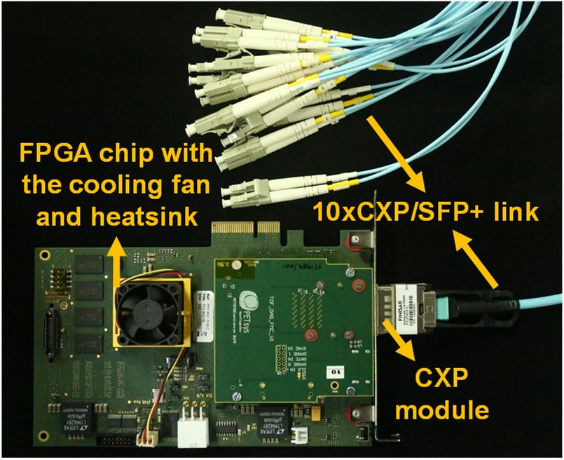
Sensors 2021, 21, x FOR PEER REVIEW                                                                                                     3 of 15

       Sensors 2021, 21, 5566                                                                                                       3 of 15
                                   transaxial FOV of the developed TOF brain PET was approximately 181 mm, covering up
                                   to the maximum size of the human brain [25].

                                           (a)                                                        (b)

                                                                     (c)
     FigureFigure
            1. (a) Geometry   of theofproposed
                   1. (a) Geometry               TOFTOF
                                       the proposed     brain  PET.
                                                            brain     (b)(b)
                                                                   PET.   Photograph
                                                                             Photographofofthe
                                                                                            thedeveloped
                                                                                                developed TOF  brain PET
                                                                                                           TOF brain PETconsisting
                                                                                                                         consistingofof 30
     detector blocks  connected  to flexible flat cables.  (c) Configuration    of the TOF   PET  detector block.
           30 detector blocks connected to flexible flat cables. (c) Configuration of the TOF PET detector block.

                                             Figure
                                        Figure       1c shows
                                                 1c shows    thethe configuration
                                                                 configuration  of of
                                                                                   thethe TOF
                                                                                        TOF    PET
                                                                                             PET     detectorblock.
                                                                                                  detector     block.Each
                                                                                                                       Each detectorblock
                                                                                                                          detector
                                       block was composed of two detector modules and a front-end module (FEM) consisting of
                                   was composed of two detector modules and a front‐end module (FEM) consisting of two
                                       two boards equipped with an application-specific integrated circuit (ASIC) chip, a SiPM
                                   boards   equipped with an application‐specific integrated circuit (ASIC) chip, a SiPM inter‐
                                       interface board, and an ASIC interface board. The two detector modules, each of which
                                   facehad
                                        board,   andofan25.8
                                            an area       ASIC   interface
                                                             × 25.8        board.
                                                                    mm2 , were    The connected
                                                                               axially  two detector   modules,
                                                                                                   to the         each ofboard
                                                                                                          SiPM interface  which  had an
                                                                                                                               with
                                   areaanofaxial
                                            25.8gap
                                                  × 25.8  mm  2, were axially connected to the SiPM interface board with an axial
                                                     of 0.6 mm. The two ASIC boards were assembled almost perpendicularly to
                                   gapboth
                                        of 0.6
                                             themm.
                                                 SiPM The  two ASIC
                                                        interface boardboards
                                                                        and thewere
                                                                                ASICassembled     almost perpendicularly to both the
                                                                                      interface board.
                                   SiPM interface board and the ASIC interface board.
                                       2.2. TOF PET Detector
                                   2.2. TOFThe
                                            PETTOF PET detector module was composed of an 8 × 8 array of 3 × 3 mm2 multi-
                                                Detector
                                      pixel photon counters (MPPCs) (S13361-3050AE-08, Hamamatsu Photonics K.K., Hama-
                                        The TOF
                                       matsu, Japan)PETanddetector  module
                                                           an 8 × 8 array     was
                                                                          of 3.11  × composed
                                                                                     3.11 × 15 mm of3 an  8 × 8 yttrium
                                                                                                      lutetium  array ofoxyorthosilicate
                                                                                                                          3 × 3 mm2 multi‐
                                   pixel photon
                                      (LYSO)       counters(Crystal
                                               scintillators  (MPPCs)    (S13361‐3050AE‐08,
                                                                     Photonics,                    Hamamatsu
                                                                                  Inc., Sanford, FL, USA), as shown Photonics
                                                                                                                       in FigureK.K., Hama‐
                                                                                                                                 2a. The
                                   matsu,  Japan)
                                       thickness ofand   an 8 ×was
                                                    the LYSO    8 array
                                                                   chosenofas3.11  × 3.11
                                                                               15 mm    by ×considering
                                                                                              15 mm lutetium
                                                                                                     3            yttrium
                                                                                                        the trade-off amongoxyorthosilicate
                                                                                                                              sensitivity,
                                   (LYSO)   scintillatorsand
                                      TOF capabilities,     (Crystal  Photonics,
                                                               parallax error [15]. Inc., Sanford, FL, USA), as shown in Figure 2a.
                                   The thickness of the LYSO was chosen as 15 mm by considering the trade‐off among sen‐
                                   sitivity, TOF capabilities, and parallax error [15].
                                         Figure 2b shows the design of the LYSO array. To achieve excellent CTR, each LYSO
                                   was mechanically polished except for a roughening entrance surface. All lateral surfaces
                                   and the entrance surface of the LYSO were optically isolated by ESR film and Teflon tape,
Feasibility Study of a Time-of-Flight Brain Positron Emission Tomography Employing Individual Channel Readout Electronics
Sensors 2021, 21, x FOR PEER REVIEW                                                                                                          4 of 15

Sensors 2021, 21, 5566                                                                                                                        4 of 15
                                      respectively. In addition, all lateral surfaces of the LYSO array were optically isolated by
                                      Teflon tape [16].

                                        (a)                                                                     (b)
       Figure2.2.(a)
      Figure      (a)88×× 88 array
                             array of
                                   of 33 ×
                                         × 33 mm
                                              mm2 MPPCs
                                                2
                                                  MPPCs (left)
                                                          (left) and
                                                                 and 88 ××88array
                                                                             arrayofof3.11
                                                                                       3.11××3.11
                                                                                               3.11× ×
                                                                                                     15 15
                                                                                                        mm mmLYSO
                                                                                                             3 3
                                                                                                                  LYSOscintillators (right).
                                                                                                                         scintillators       (b)
                                                                                                                                       (right).
       Design  of  the LYSO    array  considering optimal optical  properties  (surface  treatment    and  reflective materials).
      (b) Design of the LYSO array considering optimal optical properties (surface treatment and reflective materials).

                                            The MPPC
                                           Figure        and LYSO
                                                   2b shows           arrays
                                                              the design     ofwere  coupled
                                                                                the LYSO        using
                                                                                            array.     a silicone
                                                                                                   To achieve      adhesive
                                                                                                                excellent      (3145
                                                                                                                            CTR,       RTV,
                                                                                                                                    each    The
                                                                                                                                         LYSO
                                      Dow
                                     was     Chemical Company,
                                           mechanically   polished Midland,
                                                                      except forMI,    USA) with entrance
                                                                                   a roughening     a refractive  index All
                                                                                                               surface.   of 1.49  at 430
                                                                                                                              lateral     nm to
                                                                                                                                       surfaces
                                      match
                                     and  thethe  refractive
                                               entrance      index
                                                         surface  of between
                                                                      the LYSOoptical     boundaries
                                                                                  were optically       (MPPC:
                                                                                                    isolated  by 1.55
                                                                                                                 ESR at   450and
                                                                                                                       film    nm,Teflon
                                                                                                                                     LYSO:  1.82
                                                                                                                                          tape,
                                      at 420  nm)  taking Snell’s  law   into  account.   In addition,  this optical  coupling
                                     respectively. In addition, all lateral surfaces of the LYSO array were optically isolated by material  was
                                      used to
                                     Teflon    improve
                                             tape  [16]. the collection efficiency of scintillation light and to maintain its adhesion
                                      and The
                                            optical
                                                MPPCproperties
                                                        and LYSOfor aarrays
                                                                       long time
                                                                              were[26,27].
                                                                                    coupled using a silicone adhesive (3145 RTV, The
                                     Dow Chemical Company, Midland, MI, USA) with a refractive index of 1.49 at 430 nm to
                                      2.3. Individual
                                     match             Channel
                                             the refractive     Readout
                                                            index   betweenElectronics
                                                                                optical boundaries (MPPC: 1.55 at 450 nm, LYSO: 1.82
                                     at 420The
                                             nm)individual
                                                  taking Snell’s  law   into  account.
                                                             channel readout electronicsIn addition,
                                                                                                 were this
                                                                                                       basedoptical
                                                                                                               on a coupling
                                                                                                                     64‐channel  material  was
                                                                                                                                    commercial
                                     used
                                      ASICto(TOFPET2,
                                              improve the   collection
                                                          PETsys          efficiency
                                                                    Electronics       of scintillation
                                                                                   S.A.,               light and
                                                                                         Oeiras, Portugal)         to maintain
                                                                                                              to enable           its adhesion
                                                                                                                           fast TOF    measure‐
                                     and
                                      mentoptical  properties
                                             [28]. Figure      for a long
                                                          3 shows           time
                                                                      a block     [26,27].of the individual channel readout electronics
                                                                                diagram
                                      for the developed TOF brain PET. They were composed of the FEM, a front‐end board
                                     2.3. Individual Channel Readout Electronics
                                      (FEB) for data acquisition (DAQ) called FEB/D, a DAQ board, and a Clock&Trigger board.
                                           The individual channel readout electronics were based on a 64-channel commercial
                                     ASIC (TOFPET2, PETsys Electronics S.A., Oeiras, Portugal) to enable fast TOF measure-
                                     ment [28]. Figure 3 shows a block diagram of the individual channel readout electronics for
                                     the developed TOF brain PET. They were composed of the FEM, a front-end board (FEB)
                                     for data acquisition (DAQ) called FEB/D, a DAQ board, and a Clock&Trigger board.

                                     2.3.1. Front-End Module (FEM)
                                          As described in Section 2.1, the main components of the FEM were the ASIC board,
                                     called FEB/A, the SiPM interface board, called FEB/S, and the ASIC interface board called
                                     FEB/I [29]. FEB/A was equipped with the TOFPET2 ASIC chip, a temperature sensor, and two
                                     connectors to plug in FEB/S and FEB/I. The ASIC were low-power and low-noise electronics
                                     providing readout and digitization of signals from 64 individual channels to acquire the
                                     position, energy, and time information of an interacted gamma ray in each scintillator.
                                          As shown in Figure 4, it consisted of a preamplifier, two transimpedance amplifiers,
                                     three fast discriminators, a quad-buffered charge-to-digital converter (QDC), and a quad-
                                     buffered dual ramp time-to-digital converter (TDC) for each channel [30]. The output
                                     current signal of the detector module passed through the preamplifier, a current conveyor
                                     with low input impedance, and was then replicated to three branches: T, E, and Q. The cur-
                                     rent signals of the T and E branches were converted into voltage signals by transimpedance
                                     amplifiers, and that of the Q branch was digitized by the QDC comprising four integrators
                                     and a 10-bit Wilkinson analog-to-digital converter (ADC) for energy measurement.
                                      Figure 3. Block diagram of the individual channel readout electronics for the developed TOF brain
                                      PET.
Feasibility Study of a Time-of-Flight Brain Positron Emission Tomography Employing Individual Channel Readout Electronics
2.3. Individual Channel Readout Electronics
                        The individual channel readout electronics were based on a 64‐channel commercial
                   ASIC (TOFPET2, PETsys Electronics S.A., Oeiras, Portugal) to enable fast TOF measure‐
                   ment [28]. Figure 3 shows a block diagram of the individual channel readout electronics
Sensors 2021, 21, 5566                                                                                                                              5 of 15
                   for the developed TOF brain PET. They were composed of the FEM, a front‐end board
                   (FEB) for data acquisition (DAQ) called FEB/D, a DAQ board, and a Clock&Trigger board.

Sensors 2021, 21, x FOR PEER REVIEW                                                                                                             5 of 15

                                  2.3.1. Front‐End Module (FEM)
                                        As described in Section 2.1, the main components of the FEM were the ASIC board,
                                  called FEB/A, the SiPM interface board, called FEB/S, and the ASIC interface board called
                                  FEB/I [29]. FEB/A was equipped with the TOFPET2 ASIC chip, a temperature sensor, and
                                  two connectors to plug in FEB/S and FEB/I. The ASIC were low‐power and low‐noise elec‐
                                  tronics providing readout and digitization of signals from 64 individual channels to ac‐
                                  quire the position, energy, and time information of an interacted gamma ray in each scin‐
                                  tillator.
                                        As shown in Figure 4, it consisted of a preamplifier, two transimpedance amplifiers,
                                  three fast discriminators, a quad‐buffered charge‐to‐digital converter (QDC), and a quad‐
                                  buffered dual ramp time‐to‐digital converter (TDC) for each channel [30]. The output cur‐
                                  rent signal of the detector module passed through the preamplifier, a current conveyor
                                  with low input impedance, and was then replicated to three branches: T, E, and Q. The
                                  current signals of the T and E branches were converted into voltage signals by transim‐
                                  pedance amplifiers, and that of the Q branch was digitized by the QDC comprising four
                                  integrators and a 10‐bit Wilkinson analog‐to‐digital converter (ADC) for energy measure‐
                Figure
                     3. 3. Block
                        Block    diagram
                               diagram      of the individual channel readout electronics for the developed TOF brain
              Figure
                PET.
                                  ment.of the individual channel readout electronics for the developed TOF brain PET.

                                                             T branch                               Trigger
                                                                 VTH_T1                             signal
      Current                               Transimpedance                    Discriminator                       Delay
                       Preamplifier
       signal                                   amplifier
                                                                                                    Trigger
                                                                                                    signal
                                                                              Discriminator
                                                                 VTH_T2                                                         Logic
                                                                                                                              Controller

                                                             E branch                               Trigger
                                                                  VTH_E                             signal
                                            Transimpedance                    Discriminator
                                                amplifier

                                                             Q branch
                                                       Integrator
                                                         Integrator
                                                           Integrator
                                                                           ADC                  Energy measurement
                                                             Integrator

                                                              Quad-buffered QDC

                                                                          TAC
                                                                           TAC
                                                                            TAC           ADC        Timing measurement
                                                                              TAC

                                                                            Quad-buffered TDC

                                                        VTH_T1 = (63 – T1) × 6.5 mV, VTH_T2 = (63 – T2) × 6.5 mV, VTH_E = (63 – E) × 6.5 mV   x64
                                      Figure
                                      Figure 4.
                                             4. Block
                                                Block diagram
                                                      diagram of
                                                              of TOFPET2
                                                                 TOFPET2 ASIC
                                                                         ASIC in
                                                                              in QDC
                                                                                 QDC mode.
                                                                                     mode.

                                        The
                                        The voltage
                                             voltage signal of the T  T branch
                                                                         branch was
                                                                                  wastransferred
                                                                                        transferredto totwo
                                                                                                         twodiscriminators
                                                                                                               discriminatorseach
                                                                                                                                eachhaving
                                                                                                                                      havinga
                                  athreshold
                                     thresholdvoltage
                                                 voltagevalue, called
                                                           value,      VTH_T1
                                                                    called     , for
                                                                           VTH_T1     time
                                                                                   , for    measurement
                                                                                          time   measurementand aandthreshold  voltage
                                                                                                                       a threshold     value,
                                                                                                                                      voltage
                                   called V
                                  value,  called
                                            TH_T2 ,
                                                  V for rejecting
                                                    TH_T2, for     the
                                                               rejectingdark
                                                                          thecount
                                                                               dark   and
                                                                                       countstarting
                                                                                               and   the charge
                                                                                                    starting  the integration
                                                                                                                   charge      window.
                                                                                                                           integration    The
                                                                                                                                        win‐
                                   TDC,  which   comprised     four  time-to-amplitude        converters   (TACs)
                                  dow. The TDC, which comprised four time‐to‐amplitude converters (TACs) and a 10‐bitand a 10-bit  Wilkinson
                                   ADC, was ADC,
                                  Wilkinson    used forwastime
                                                            usedmeasurement.      The voltageThe
                                                                   for time measurement.          signal  of thesignal
                                                                                                      voltage     E branch  was
                                                                                                                       of the     transferred
                                                                                                                              E branch   was
                                   to a discriminator
                                  transferred            with a threshold
                                                to a discriminator      with voltage
                                                                              a thresholdvalue,  calledvalue,
                                                                                               voltage   VTH_E ,called
                                                                                                                  for rejecting  lowrejecting
                                                                                                                         VTH_E, for   voltage
                                  low voltage signal. All threshold voltage values were set by DAQ software as digital val‐
                                  ues, called T1, T2, and E, as follows:
                                                                            VTH_T1 = (63 − T1) × 6.5 mV                                                (1)
Feasibility Study of a Time-of-Flight Brain Positron Emission Tomography Employing Individual Channel Readout Electronics
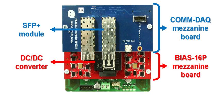
Sensors 2021, 21, 5566                                                                                          6 of 15

                         signal. All threshold voltage values were set by DAQ software as digital values, called T1,
                         T2, and E, as follows:
                                                        VTH_T1 = (63 − T1) × 6.5 mV                              (1)
                                                            VTH_T2 = (63 − T2) × 6.5 mV                            (2)
                                                             VTH_E = (63 − E) × 6.5 mV                             (3)
                              Trigger signals output from these discriminators were transferred to a logic controller.
                         The logic controller activated the QDC and TDC under certain conditions and determined
                         that the detected gamma ray was a valid event when all trigger signals were on the rising
                         edge. The raw data, including information about valid events, were transmitted to the
                         ASIC interface board through four LVDS output links with a maximum data rate per
                         link of 800 Mbit/s and a maximum output event rate per channel was 0.6 kevent/s. The
                         specifications of the ASIC are summarized in Table 1.

                         Table 1. Brief specifications of the ASIC.

                                            Description                             TOFPET2 (Version 2c)
                                           Technology                                      110 nm CMOS
                                         Supply voltage                                      1.2 V, 2.5 V
                                       Power consumption                                  8.2 mW/channel
                                      Main clock frequency                                     400 MHz
                                      TDC clock frequency                                      200 MHz
                                          TDC time bin                                           31 ps
                                         TDC resolution                                     20 ps (r.m.s.)
                                      QDC dynamic range                                       0–1500 pC
                                       Maximum data rate                                      3.2 Gbit/s
                                    Maximum output event rate                               40 Mevent/s

                              FEB/S was equipped with connectors for transmission of 128 output signals of two
                         MPPC arrays to two FEB/As, and two sensors for monitoring of the temperature of two
                         MPPC arrays. FEB/I managed the communication between the two FEB/As and FEB/D
                         through a 50 cm-long flexible flat cable connected to an on-board FEM port.

                         2.3.2. Front-End Board for Data Acquisition (FEB/D)
                              Figure 5 shows FEB/D comprising a motherboard, a BIAS-16P mezzanine board, and
                         a COMM-DAQ mezzanine board [29,31]. The motherboard was equipped with a field
                         programmable gate array (FPGA) chip, and eight FEM ports for operating up to eight
                         FEMs through 50 cm-long flexible flat cables. The role of the motherboard was to distribute
                         power, clock, and configuration signals to each FEM, to receive temperature values and
                         raw data on the ASIC from each FEM, and to collect raw data into data frames, as shown
                         in Figure 3. The motherboard only required a single external supply voltage of 12 V with a
                         maximum current of 4 A and used a set of switching regulators to supply power to eight
                         FEMs as well as the entire FEB/D.
                              The BIAS-16P mezzanine board supplied voltage to 16 MPPC arrays through two
                         on-board DC/DC converters, each with a maximum current of 20 mA. Each DC/DC
                         converter provided eight positive voltage lines capable of independent voltage settings
                         within the range 0–72 V by DAQ software, with an average current per line of 2.5 mA.
                              The COMM-DAQ mezzanine board was equipped with an enhanced small form-
                         factor pluggable (SFP+) optical transceiver module for transmission of data frames to the
                         DAQ board and receipt of configuration signals from the DAQ board. The communication
                         between the COMM-DAQ mezzanine board and the DAQ board was through the SFP+
                         high-speed serial optical link. The maximum output event rate per link was 100 Mevent/s
                         at up to 6.6 Gbit/s. In addition, the COMM-DAQ mezzanine board was equipped with a
                         small multiple connector type Q (SMC-Q) for receipt of clock, synchronization, and trigger
                         signals from the Clock&Trigger board through a 2 m-long flat cable assembly.
Feasibility Study of a Time-of-Flight Brain Positron Emission Tomography Employing Individual Channel Readout Electronics
programmable gate array (FPGA) chip, and eight FEM ports for operating up to eight
                                    FEMs through 50 cm‐long flexible flat cables. The role of the motherboard was to distrib‐
                                    ute power, clock, and configuration signals to each FEM, to receive temperature values
Sensors 2021, 21, x FOR PEER REVIEW and raw data on the ASIC from each FEM, and to collect raw data into data frames,             7 ofas15
Sensors 2021, 21, 5566              shown in Figure 3. The motherboard only required a single external supply voltage of7 of         1215
                                    V with a maximum current of 4 A and used a set of switching regulators to supply power
                                    to eight FEMs as well as the entire FEB/D.
                                           The BIAS‐16P mezzanine board supplied voltage to 16 MPPC arrays through two on‐
                                     board DC/DC converters, each with a maximum current of 20 mA. Each DC/DC converter
                                     provided eight positive voltage lines capable of independent voltage settings within the
                                     range 0–72 V by DAQ software, with an average current per line of 2.5 mA.
                                           The COMM‐DAQ mezzanine board was equipped with an enhanced small form‐fac‐
                                     tor pluggable (SFP+) optical transceiver module for transmission of data frames to the
                                     DAQ board and receipt of configuration signals from the DAQ board. The communication
                                     between the COMM‐DAQ mezzanine board and the DAQ board was through the SFP+
                                     high‐speed serial optical link. The maximum output event rate per link was 100 Mevent/s
                                     at up to 6.6 Gbit/s. In addition, the COMM‐DAQ mezzanine board was equipped with a
                                   (a)small multiple connector type Q (SMC‐Q) for receipt of clock,     (b) synchronization, and trigger
                Figure               signals
                  Figure5.5.Photographs
                             Photographs       fromcapable
                                         ofofFEB/D
                                              FEB/D the Clock&Trigger
                                                           ofof
                                                     capable  connecting board    through
                                                                         upuptotoeight
                                                                connecting                  a front
                                                                                   eightFEMs:
                                                                                         FEMs:2 front
                                                                                                 m‐long     flat
                                                                                                    (a)(a)and
                                                                                                           and   cable
                                                                                                               back (b)
                                                                                                                 back   assembly.
                                                                                                                        views.
                                                                                                                      (b) views.

                                  2.3.3.
                                  2.3.3. DAQ
                                         DAQ Board
                                             Board and
                                                   and Clock&Trigger
                                                       Clock&Trigger Board
                                       As
                                       As shown
                                           shown in in Figure 6a, the DAQ board was equipped with an FPGA chip and a
                                  CoaXPress
                                  CoaXPress (CXP) optical transceiver module
                                                                           module capable
                                                                                    capable of connecting
                                                                                                 connecting up
                                                                                                             up to 12 SFP+ modules
                                  through a 5 m-long
                                  through      m‐long 12xCXP/SFP+
                                                         12xCXP/SFP+ linklink[32].
                                                                              [32].The
                                                                                     TheDAQDAQboard
                                                                                                 board was
                                                                                                         was mounted
                                                                                                             mounted on   on a PCIe 2.0
                                  x4 slot on a computer to be operated and controlled. The      The role of the DAQ board was to
                                  generate signals for ASIC
                                  generate               ASIC configuration,
                                                                configuration, to run the
                                                                                        the calibration
                                                                                            calibration process
                                                                                                         process for transimpedance
                                                                                                                       transimpedance
                                  amplifiers,
                                  amplifiers, discriminators,    QDCs,  and  TDCs,
                                                                             TDCs, to receive data frames from FEB/Ds, to store
                                                                                     to  receive data  frames from    FEB/Ds,
                                  them on the computer,
                                  them         computer, andandtotoconvert
                                                                    convertthem
                                                                            theminto
                                                                                   intobinary
                                                                                         binarylist-mode
                                                                                                 list‐modedata,
                                                                                                            data,asasshown
                                                                                                                      shownininFigure 3.
                                                                                                                                 Figure
                                  The
                                  3.   DAQ
                                     The  DAQboard   alsoalso
                                                 board    monitored   the values
                                                               monitored          of theoftemperature
                                                                           the values                    sensorssensors
                                                                                            the temperature       mounted     on FEB/S
                                                                                                                           mounted   on
                                  and FEB/A.
                                  FEB/S         All of All
                                         and FEB/A.    theseoffunctions were controlled
                                                               these functions              by DAQbysoftware
                                                                                were controlled                run on 64-bit
                                                                                                        DAQ software      run onCentOS
                                                                                                                                  64‐bit
                                  7 Linux 7[33].
                                  CentOS         The[33].
                                             Linux    maximum      output event
                                                           The maximum           rate
                                                                            output     fromrate
                                                                                     event    the from
                                                                                                   DAQtheboard
                                                                                                            DAQ to board
                                                                                                                    the computer    was
                                                                                                                            to the com‐
                                  250 Mevent/s.
                                  puter was 250 Mevent/s.

                                     (a)                                                      (b)
     Figure 6. Photographs
     Figure 6. Photographs of
                            of the
                                the DAQ
                                    DAQ board
                                        board (a)
                                              (a) and
                                                  and the
                                                       the Clock&Trigger board (b).
                                                           Clock&Trigger board (b). For
                                                                                    For the
                                                                                        the developed
                                                                                            developed TOF
                                                                                                      TOF brain
                                                                                                          brain PET,
                                                                                                                PET, aa
     10xCXP/SFP+  link was used  to communicate with the DAQ  board.
     10xCXP/SFP+ link was used to communicate with the DAQ board.

                                       Figure
                                       Figure 6b shows
                                                   shows the
                                                           the Clock&Trigger board comprising the same motherboard and
                                  COMM‐DAQ        mezzanineboard
                                  COMM-DAQ mezzanine           boardasasFEB/D
                                                                         FEB/Dand and1616SMC-Qs
                                                                                          SMC‐Qs[32].[32].The
                                                                                                           Therole
                                                                                                                roleofofthe
                                                                                                                          the Clock&Trig‐
                                                                                                                            Clock&Trigger
                                  ger board   was  to generate   the system    reference   clock of  200  MHz,    synchronization,
                                  board was to generate the system reference clock of 200 MHz, synchronization, and trigger            and
                                  trigger signals  and  to send   them   to  up  to 16  FEB/Ds,   as  shown    in  Figure
                                  signals and to send them to up to 16 FEB/Ds, as shown in Figure 3. All boards equipped     3. All boards
                                  equipped
                                  with FPGA  with  FPGA
                                               chips  werechips   were programmed
                                                            programmed                   with
                                                                              with bit files   bit files implemented
                                                                                             implemented     to performtothe   perform  the
                                                                                                                                 functions
                                  functions  of each
                                  of each board       boardthe
                                                  through   through    the standard
                                                                standard               JTAG interface.
                                                                            JTAG interface.    All of theAll  of the
                                                                                                           FPGA        FPGA
                                                                                                                    chips   werechips were
                                                                                                                                  Kintex-7
                                  Kintex‐7  FPGAs (XC7K160T,
                                  FPGAs (XC7K160T,                  Xilinx,
                                                        Xilinx, Inc.,        Inc.,CA,
                                                                      San Jose,    SanUSA).
                                                                                        Jose, CA,   USA). Ineach
                                                                                               In addition,     addition,
                                                                                                                    of these each  of these
                                                                                                                                boards was
                                  equipped
                                  boards  waswith  a cooling
                                               equipped       fana and
                                                           with         heatsink
                                                                   cooling         forheatsink
                                                                             fan and   dissipation
                                                                                                 for of the heat from
                                                                                                      dissipation   of the the FPGA
                                                                                                                             heat fromchip.
                                                                                                                                        the
                                  FPGA chip.
Feasibility Study of a Time-of-Flight Brain Positron Emission Tomography Employing Individual Channel Readout Electronics
Before evaluating the feasibility of the TOF brain PET employing indiv
                         readout electronics, the ASIC calibration process was performed at room
                         with a breakdown voltage of the MPPC set to 53 V. All experiments were a
Sensors 2021, 21, 5566                                                                                           8 of 15
                         at room temperature and the TOF PET detector blocks were cooled using a
                         The binary list‐mode data acquired using the developed TOF brain PET we
                         prompt      coincidence
                         2.4. Performance  Evaluation data considering the energy window of 10%, the coinc
                         window        of 5 ns (without
                               Before evaluating              time
                                                  the feasibility     offset
                                                                  of the      correction),
                                                                         TOF brain          and individual
                                                                                   PET employing    all possible
                                                                                                             channel LORs ac
                         The   acquired
                         readout             energy
                                   electronics,        spectra
                                                the ASIC          wereprocess
                                                           calibration    not corrected   for the
                                                                                was performed       energy
                                                                                                at room      nonlinearity
                                                                                                         temperature
                         with a breakdown voltage of the MPPC set to 53 V. All experiments were also carried out
                         the SiPM saturation and the nonlinear QDC response. All tomographic ima
                         at room temperature and the TOF PET detector blocks were cooled using air circulation.
                         TOF    images
                         The binary         reconstructed
                                      list-mode  data acquired without      attenuation,
                                                                 using the developed       normalization,
                                                                                     TOF brain  PET were sortedscatter,
                                                                                                                   into  and
                         rections.
                         prompt   coincidence   data considering   the energy window  of 10%, the  coincidence timing
                         window of 5 ns (without time offset correction), and all possible LORs across the FOV. The
                         acquired energy spectra were not corrected for the energy nonlinearity resulting from the
                         2.4.1. Energyand
                         SiPM saturation  Resolution,    Coincidence
                                             the nonlinear  QDC response.Counting         Rate,
                                                                             All tomographic     and were
                                                                                              images   Coincidence
                                                                                                            nonTOF           Tim
                         Resolution
                         images reconstructed without attenuation, normalization, scatter, and random corrections.

                                As shown
                         2.4.1. Energy       in Figure
                                       Resolution,        7, a Counting
                                                   Coincidence 1.8 MBqRate,
                                                                        of and
                                                                            NaCoincidence
                                                                               point source
                                                                                  22
                                                                                          Timinghaving   an
                                                                                                 Resolution         active
                          mmAs  was   placed
                                   shown         at the
                                          in Figure  7, acenter
                                                          1.8 MBqbetween     a pair
                                                                  of 22 Na point     of having
                                                                                 source  channels,  anddiameter
                                                                                               an active the dataof were a
                         1the
                            mm   wasof
                               pair   placed  at the center
                                        channels     of two  between a pair
                                                               detector     of channels,
                                                                         modules         and each
                                                                                     facing  the data wereon
                                                                                                   other   acquired
                                                                                                              the TOF bra
                          using the pair of channels of two detector modules facing each other on the TOF brain PET
                          s.
                          for 240 s.

                         Figure 7. Experimental setup to evaluate the performance (energy resolution, CCR, and CTR) of the
                         Figure   7. Experimental setup to evaluate the performance (energy resolution, CCR,
                         detector module. The 22 Na point source was placed at the center between a pair of channels.
                         detector module. The 22Na point source was placed at the center between a pair of c
                               The energy resolution was measured by calculating the full width at half maximum
                         (FWHM) using a Gaussian fit to the photopeak position corresponding to 511 keV in
                                 The energy resolution was measured by calculating the full width at h
                         the energy spectrum acquired with energy values of the list-mode data. The CCR was
                         (FWHM)
                         measured byusing       a Gaussian
                                        calculating             fit toofthe
                                                    the total number         photopeak
                                                                         prompt             position
                                                                                  coincidence           corresponding
                                                                                               data detected during the     to 5
                         data acquisition
                         energy            time. The
                                     spectrum         CTR waswith
                                                  acquired      measured   by calculating
                                                                      energy     values the
                                                                                          of FWHM     using a Gaussian
                                                                                              the list‐mode     data. The C
                         fit to the coincidence peak position in the time spectrum acquired with the difference in
                         ured     by calculating the total number of prompt coincidence data detected d
                         time values of the prompt coincidence data.
                         acquisition
                               To optimizetime.   The CTRofwas
                                            the performance           measured
                                                                 the detector       bythe
                                                                              module,    calculating    the FWHM
                                                                                           energy resolution, CCR, and using
                         CTR   were   measured  (repeated three  times) while changing
                         to the coincidence peak position in the time spectrum acquired the overvoltage  (V     ) of thethe diff
                                                                                                           OVERwith
                         MPPC and T1 of the ASIC. The VOVER and T1 values were set at 1 V increments from 1 to
                         values     of the prompt coincidence data.
                         7 V and five increments from 20 to 60, respectively. The optimal VOVER and T1 values were
                                 To optimize
                         determined    consideringthe performance
                                                    average              ofenergy
                                                             values of the  the detector
                                                                                   resolution,module,
                                                                                               CCR, and the
                                                                                                         CTR.energy resolut
                         CTR were measured (repeated three times) while changing the overvoltage
                         MPPC and T1 of the ASIC. The VOVER and T1 values were set at 1 V increm
                         7 V and five increments from 20 to 60, respectively. The optimal VOVER and T
                         determined considering average values of the energy resolution, CCR, and
Feasibility Study of a Time-of-Flight Brain Positron Emission Tomography Employing Individual Channel Readout Electronics
Sensors 2021, 21, 5566                                                                                            9 of 15

                         2.4.2. Spatial Resolution
                              In order to evaluate the spatial resolution of the TOF brain PET, the data were acquired
                         using the 1.7 MBq of 22 Na point source placed at the center of the FOV for 240 s. In addition,
                         the data acquisition was repeated while moving the same point source to the following
                         transaxial distances from the center: 20, 40, 60, and 80 mm. The tomographic images of
                         the point source were reconstructed by a 2-dimensional filtered backprojection algorithm
                         with a Hann filter (cut-off frequency = 0.42 × Nyquist frequency) and 514 × 514 pixels
                         of 0.5 × 0.5 mm2 . The spatial resolution was measured by calculating the FWHM using
                         a Gaussian fit to each pixel peak position in response functions (1-dimensional profiles)
                         acquired with the reconstructed images of the point source.

                         2.4.3. Phantom Imaging
                               The data were acquired using a custom-made hot-rod phantom filled with 10.4 MBq
                         of 18 F placed at the center of the FOV to evaluate the imaging capability of the TOF brain
                         PET for 120 s. The diameter and height of the hot-rod phantom were 75 and 40 mm,
                         respectively, and it consisted of 40 rods with different diameters (2.5, 3.5, 4.5, 5.5, and
                         6.5 mm). The tomographic images of the hot-rod phantom were reconstructed by a
                         3-dimensional maximum-likelihood expectation-maximization algorithm with 31 itera-
                         tions and 514 × 514 × 514 voxels of 0.5 × 0.5 × 0.5 mm3 .

                         3. Results
                         3.1. Energy Resolution, Coincidence Counting Rate, and Coincidence Timing Resolution
                              Figure 8 shows average values of the photopeak position, energy resolution, CCR, and
                         CTR measured using a pair of channels at different VOVER and T1 values. The average pho-
                         topeak position was almost linearly shifted to higher QDC values with increasing VOVER
                         value, regardless of the T1 value (Figure 8a). The average energy resolution gradually
                         improved as the VOVER value increased, but rapidly deteriorated after the VOVER value of
                         5–6 V (Figure 8b). The average CCR increased, but the rate of change gradually decreased
                         as the VOVER value increased (Figure 8c). In addition, like the average energy resolution,
                         the effect of the T1 value on the average CCR was relatively small. The average CTR
                         improved as the VOVER value increased, but rapidly deteriorated after the VOVER value
                         of 5–6 V (Figure 8d). At the VOVER values of 5 and 6 V (T1 = 30), the average CTRs were
                         195.5 ± 9.2 and 194.7 ± 12.1 ps FWHM, respectively.
                              The optimal VOVER and T1 values were determined to be 5 V and 30, respectively,
                         considering the standard deviation of the CTR. The average values of the photopeak
                         position, energy resolution, and CCR were 335 ± 3, 5.6 ± 1.4% FWHM (without energy
                         nonlinearity correction), and 6.1 ± 0.2 cps, respectively at the optimal values. The best CTR
                         of 187 ps FWHM was achieved, as shown in Figure 9.
                              Figure 10 shows the representative energy spectra of 64 channels (one of 60 detector
                         modules) among the energy spectra of 3840 channels acquired with the TOF brain PET
                         using the 22 Na point source placed at the center of the FOV to evaluate the spatial resolution.
                         The average energy resolution and CCR of the 3840 channels were 6.6 ± 0.6% FWHM (not
                         corrected for the energy nonlinearity) and 13.3 kcps at 1.7 MBq, respectively.
Feasibility Study of a Time-of-Flight Brain Positron Emission Tomography Employing Individual Channel Readout Electronics
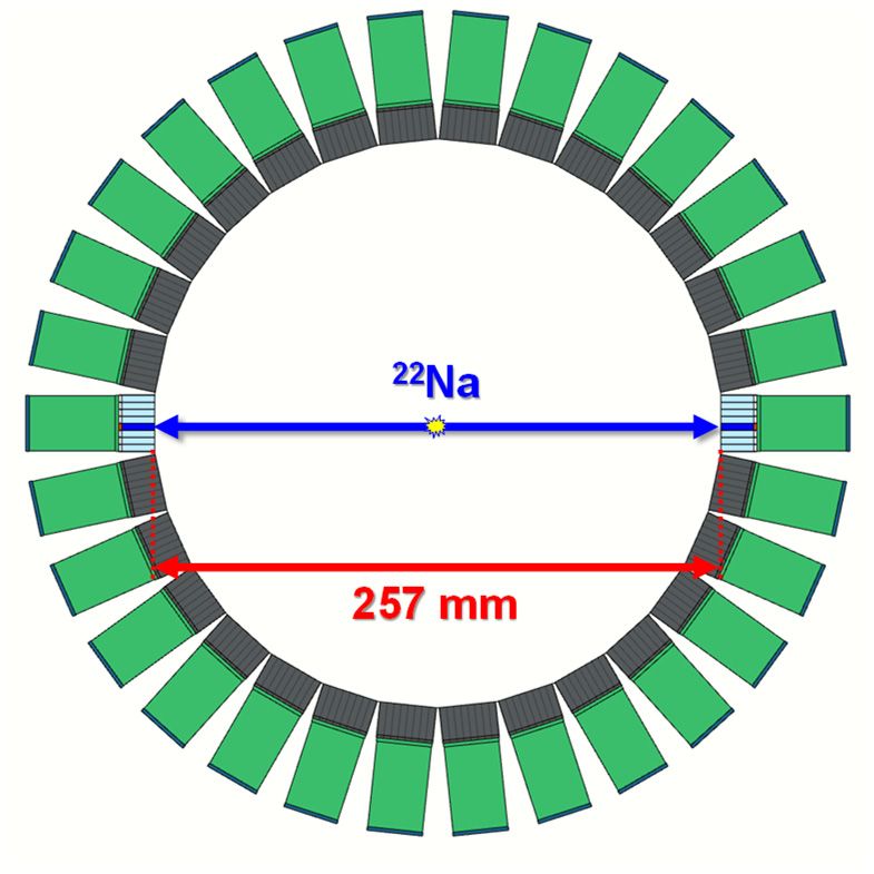
of 5–6 V (Figure 8b). The average CCR increased, but the rate of change gradually de‐
                                creased as the VOVER value increased (Figure 8c). In addition, like the average energy res‐
                                olution, the effect of the T1 value on the average CCR was relatively small. The average
ors 2021, 21, x FOR PEER REVIEW CTR  improved as the VOVER value increased, but rapidly deteriorated after the VOVER value
        Sensors 2021, 21, 5566  of 5–6 V (Figure 8d). At the VOVER values of 5 and 6 V (T1 = 30), the average CTRs10were
                                                                                                                       of 15
                                195.5 ± 9.2 and 194.7 ± 12.1 ps FWHM, respectively.

                                                                                                                                               Average energy resolution (% FWHM)
                                                                  500                                                                                                                 9
                              Average photopeak position (a.u.)

                                                                                                                                                                                                                                                                         T1 = 60
                      7                                                                                                                                                                               280                                                                T1 = 55
                                                                                                                                                                                      8                                                                                  T1 = 50
                                                                  400                                                                                                                                                                                                    T1 = 45

                                                                                                                                                                          Average CTR (ps FWHM)
                                                                                                                                                                                                                                                                         T1 = 40
                                                                                                                                                                                                      260                                                                T1 = 35
  Average CCR (cps)

                      6                                                                                                                                                               7
                                                                                                                                                                                                                                                                         T1 = 30
                                                                  300                                                                                                                                                                                                    T1 = 25
                                                                                                                                                                                      6               240                                                                T1 = 20

                      5                                           200
                                                                                                                                                                                      5
                                                                                                                                                                                                      220
                                10021, x FOR PEER REVIEW
                      Sensors 2021,                                                                                                                                                   4                                                                                      10 of 15
                      4             0      1   2    3    4                                          5   6     7    8                                                                              0         1   2       3         4         5     6        7        8
                                                                                      VOVER (V)
                                                                                                                                                                                                      200                   VOVER (V)

                                                                                      (a)                                                                                                                                             (b)
                      3                                                                                                                                                                               180
                          0                                       17    2   3         4         5       6     7        8                               280
                                                                                                                                                                                                            0       1         2             3         4         5       6 = 60
                                                                                                                                                                                                                                                                        T1         7    8
                                                                                                                                                                                                                                                                        T1 = 55
                                                                                VOVER (V)                                                                                                                                                       VOVER (V)
                                                                                                                       Average CTR (ps FWHM)

                                                                                                                                                       260                                                                                                              T1 = 50
                                              Average CCR (cps)

                                                                   6                                                                                                                                                                                                    T1 = 45
                                                                                                                                                                                                                                                                        T1 = 40
                                                                                (c)                                                                                                                                                                       (d)           T1 = 35
                                                                                                                                                       240
                                                                                                                                                                                                                                                                        T1 = 30
               5
 Figure 8. Average   photopeak position (a), energy resolution (b), CCR (c), and CTR (d) measured using a pair of ch                                                                                                                                                    T1 = 25
                                                         220                                                                                                                                                                                                            T1 = 20
 at different VOVER and T1 values.
                                                                   4
                                                                                                                                                       200
                                                             The optimal VOVER and T1 values were determined to be 5 V and 30, re
                                   3                  considering the standard180          deviation of the CTR. The average values of the pho
                                     0     1    2    3     4     5    6     7    8            0    1      2   3     4     5   6    7     8
                                                      sition,
                                                       VOVER (V)energy resolution, and CCR wereVOVER             335 (V)
                                                                                                                       ± 3, 5.6 ± 1.4% FWHM (without e
                                                      linearity
                                                       (c)         correction), and 6.1 ± 0.2 cps, respectively       (d)     at the optimal values. The b
                                                      187 ps FWHM was achieved, as shown in Figure 9.
                               Figure 8. Average photopeak position (a), energy resolution (b), CCR (c), and CTR (d) measured using a pair of channels
                                Figure 8. Average photopeak position (a), energy resolution (b), CCR (c), and CTR (d) measured using a pair of channels at
                               atdifferent        andT1
                                  differentVVOVER and T1values.
                                                        values.
                                            OVER

                                                                                               The optimal VOVER and T1 values were determined to be 5 V and 30, respectively,
                                                                                          considering the standard deviation of the CTR. The average values of the photopeak po‐
                                                                                          sition, energy resolution, and CCR were 335 ± 3, 5.6 ± 1.4% FWHM (without energy non‐
                                                                                          linearity correction), and 6.1 ± 0.2 cps, respectively at the optimal values. The best CTR of
                                                                                          187 ps FWHM was achieved, as shown in Figure 9.

                                                                                            Figure 9. Time spectrum acquired at the VOVER of 5 V and T1 of 30. The solid line was the result of
                                                                                  Figure 9. Time spectrum acquired at the VOVER of 5 V and T1 of 30. The solid line was
                                                                                     applying a Gaussian fit to the coincidence peak position.
                                                                                  applying a Gaussian fit to the coincidence peak position.
                                                                                          Figure 9. Time spectrum acquired at the VOVER of 5 V and T1 of 30. The solid line was the result of
                                                                                          applying a Gaussian fit to the coincidence peak position.
                                                                                      Figure 10 shows the representative energy spectra of 64 channels (one of
                                                                                  modules)   among
                                                                                        Figure  10 showsthe
                                                                                                          the energy   spectra
                                                                                                              representative      ofspectra
                                                                                                                             energy  3840 ofchannels   acquired
                                                                                                                                              64 channels (one of 60 with   the TOF
                                                                                                                                                                     detector
                                                                                  using the among
                                                                                    modules) 22Na point     source
                                                                                                      the energy     placed
                                                                                                                  spectra      at channels
                                                                                                                          of 3840 the center   of the
                                                                                                                                           acquired   FOV
                                                                                                                                                    with     to evaluate
                                                                                                                                                         the TOF   brain PET the spa
Sensors 2021, 21, 5566                                                                                                                11 of 15
Sensors 2021, 21, x FOR PEER REVIEW                                                                                                                11 of 15
   Sensors 2021, 21, x FOR PEER REVIEW                                                                                                  11 of 15

        Figure 10. Representative energy spectra acquired from 64 channels of the TOF brain PET. The thick solid lines were the
        result of applying
           Figure          a Gaussian energy
                   10. Representative fit to thespectra
                                                 photopeak  position
                                                        acquired fromcorresponding
                                                                      64 channels oftothe
                                                                                        511 keV.
                                                                                          TOF brain PET. The thick solid lines were the
     Figure 10. Representative energy spectra acquired from 64 channels of the TOF brain PET. The thick solid lines were the
           result of applying a Gaussian fit to the photopeak position corresponding to 511 keV.
     result of applying a Gaussian fit Spatial
                                 3.2.  to the photopeak
                                               Resolution position corresponding to 511 keV.
                                       3.2. Spatial
                                         Figure  11 Resolution
                                                    shows the spatial resolution of the TOF brain PET as a function of the trans‐
                                   3.2. Spatial Resolution
                                    axial distance from the center of the FOV. A transaxial spatial resolution of 2.5 mm FWHM
                                             Figure 11 shows the spatial resolution of the TOF brain PET as a function of the
                                         Figure
                                    wastransaxial
                                         achieved11distance
                                                    atshows   the
                                                              fromspatial
                                                        the center ofthe    resolution
                                                                      thecenter
                                                                          axial and      of the
                                                                                              A TOF
                                                                                     transaxial
                                                                                 of the FOV.    FOV.brainspatial
                                                                                                transaxial  PET asresolution
                                                                                                                    a function
                                                                                                                             of of
                                                                                                                                2.5the
                                                                                                                                    mm trans‐
                                   axialFWHM
                                         distance
                                                wasfrom     the center
                                                       achieved          of the of
                                                                 at the center  FOV.   A transaxial
                                                                                   the axial         spatialFOV.
                                                                                             and transaxial  resolution of 2.5 mm FWHM
                                   was achieved at the center of the axial and transaxial FOV.
                                                                                  4.5
                                                                      (mm FWHM)

                                                                                  4.0
                                                                                  4.5
                                                             (mm FWHM)

                                                                                  3.5
                                                                                  4.0
                                                   Spatial resolution

                                                                                  3.0
                                                                                  3.5
                                         Spatial resolution

                                                                                  2.5
                                                                                  3.0
                                                                                  2.0
                                                                                    –20     0      20     40     60      80    100
                                                                                  2.5
                                                                                  Transaxial distance from the center of the FOV (mm)

                                    Figure  2.0Spatial
                                           11.
                                       Figure           resolution
                                                11. Spatial        of the
                                                            resolution    TOFTOF
                                                                       of the brain PETPET
                                                                                 brain  as aasfunction  of the
                                                                                                a function      transaxial
                                                                                                            of the         distance
                                                                                                                   transaxial       from
                                                                                                                               distance   the the
                                                                                                                                        from
                                    center       20the
                                               –of
                                           of the
                                       center      FOV.   0
                                                       FOV.       20       40    60      80        100
                                            Transaxial distance from the center of the FOV (mm)
                                    3.3.3.3. Phantom
                                         Phantom      Imaging
                                                   Imaging
                                   FigureFigure
                                            11. Spatial
                                              Figure 12 resolution
                                                        shows
                                                  12 shows          of the TOF
                                                                a tomographic
                                                             a tomographic      brainofPET
                                                                                image
                                                                              image    of   as
                                                                                          the
                                                                                        the    a function
                                                                                              hot-rod
                                                                                            hot‐rod        of thewith
                                                                                                       phantom
                                                                                                     phantom      transaxial
                                                                                                                  withaabit   distance
                                                                                                                         bitdepth
                                                                                                                             depth     from the
                                                                                                                                    of8‐
                                                                                                                                   of 8-bit
                                   center  of the
                                        acquired  FOV.
                                    bit acquired using the TOF brain PET. The rods were clearly resolved down to a diameter of
                                                   using  the TOF   brain PET. The rods   were  clearly resolved  down   to  a diameter
                                        2.5mm
                                    of 2.5   mmininthe
                                                    thehot‐rod
                                                        hot-rodphantom
                                                                 phantomimage.
                                                                            image.
                                   3.3. Phantom Imaging
                                        Figure 12 shows a tomographic image of the hot‐rod phantom with a bit depth of 8‐
                                   bit acquired using the TOF brain PET. The rods were clearly resolved down to a diameter
                                   of 2.5 mm in the hot‐rod phantom image.
s 2021, 21, x FOR
         Sensors    PEER
                 2021,       REVIEW
                       21, 5566                                                                                                         12 of 15       12

                                            (a)                                                          (b)
            Figure
Figure 12. (a)     12. (a) Photograph
                Photograph       of theofhot‐rod
                                           the hot-rod phantom comprising
                                                    phantom    comprising 40 rods with different
                                                                              40 rods            diameters (2.5,
                                                                                        with different           3.5, 4.5, 5.5,
                                                                                                           diameters            and3.5,
                                                                                                                            (2.5,   6.5 mm).
                                                                                                                                         4.5, 5.5, and 6.5
            (b) Transverse  slice of the hot-rod phantom  image acquired using the TOF
mm). (b) Transverse slice of the hot‐rod phantom image acquired using the TOF brain PET.brain PET.

                                           4. Discussion
                                  4. Discussion
                                           In this study, we have developed a TOF brain PET by employing an optimal geometry
                                        Into this
                                             improve     sensitivity,
                                                    study,    we have  a fast TOF PET detector
                                                                            developed         a TOFtobrain
                                                                                                         achieve excellent
                                                                                                               PET           CTR, and individual
                                                                                                                      by employing         an optimal ge
                                          channel readout electronics to enable TOF measurement. The feasibility of the TOF brain
                                  try to improve sensitivity, a fast TOF PET detector to achieve excellent CTR, and ind
                                          PET has been evaluated by measuring the energy resolution, CCR, CTR, and spatial
                                  ual channel
                                          resolution.readout      electronics
                                                        Tomographic      images ofto  theenable     TOF hot-rod
                                                                                          custom-made      measurement.
                                                                                                                   phantom have Thebeen
                                                                                                                                      feasibility
                                                                                                                                           acquired of the
                                  brain toPET     has been
                                              evaluate          evaluated
                                                         the imaging            by measuring
                                                                          capability                  the energy
                                                                                       of the TOF brain     PET. Theresolution,
                                                                                                                        image qualityCCR,     CTR, and sp
                                                                                                                                        phantoms
                                  resolution. Tomographic images of the custom‐made hot‐rod phantom not
                                          specified   in the  national  electrical   manufacturers     association (NEMA)     standards   were    have bee
                                          used because it is not fully functional but a proof-of-principle system demonstrating the
                                  quiredfeasibility
                                            to evaluate        the imaging capability of the TOF brain PET. The image quality p
                                                       of the TOF brain PET. The developed TOF brain PET has the potential to improve
                                  toms sensitivity,
                                          specifiedspatialin the     national
                                                                 resolution,   andelectrical
                                                                                     image quality manufacturers         association
                                                                                                      compared to a conventional          (NEMA) stand
                                                                                                                                      whole-body
                                  were notPET in used
                                                    brainbecause
                                                            imaging itdue istonot
                                                                               the fully
                                                                                     reduced functional     butthe
                                                                                                ring diameter,    a proof‐of‐principle
                                                                                                                     detector size, and the TOF system de
                                          capabilities. It is expected that the TOF brain PET will provide better system performance
                                  strating the feasibility of the TOF brain PET. The developed TOF brain PET has the p
                                          than a conventional PET employing a multiplexing circuit that reduces the number of
                                  tial toreadout
                                           improve        sensitivity,
                                                     channels   but degradesspatial     resolution,
                                                                                 the overall             and ofimage
                                                                                                performance               quality compared to a con
                                                                                                                 the detector.
                                  tional whole‐body
                                                The arrival timePETofinthebrain
                                                                            detected imaging
                                                                                       gamma ray   duewastomeasured
                                                                                                             the reduced       ring diameter,
                                                                                                                      by a leading-edge    discrimi-the det
                                          nation
                                  size, and        method
                                                 the   TOFusing     the discriminator
                                                               capabilities.              in the individual
                                                                                  It is expected        that channel
                                                                                                              the TOF  readout  electronics,
                                                                                                                            brain  PET will   which
                                                                                                                                                 provide b
                                          could cause timing walk, an energy-dependent timing variation, leading to degradation of
                                  system     performance than a conventional PET employing a multiplexing circuit th
                                          the CTR [9,34]. There are two general ways to reduce it. One is to increase the amplitude
                                  ducesofthe  thenumber       of readout
                                                   output signal   of the SiPM channels
                                                                                    input tobut     degrades theand
                                                                                               the discriminator,     overall    performance
                                                                                                                          the other is to decreaseof the d
                                  tor. the threshold voltage value of the discriminator. In general, for the former, it is necessary
                                          to increase
                                        The     arrivalthe    operating
                                                           time   of thevoltage
                                                                            detected of the  SiPM orray
                                                                                          gamma         thewas
                                                                                                            gain measured
                                                                                                                 of the amplifier,
                                                                                                                                by awhich    causes
                                                                                                                                      leading‐edge      dis
                                          an increase in the dark count or the amplitude of noise. In the latter case, as the value
                                  ination     method
                                          continues         using the
                                                       to decrease,         discriminator
                                                                      the arrival   time of the in darkthe  individual
                                                                                                         count rather than channel
                                                                                                                             the detectedreadout
                                                                                                                                            gamma electro
                                  whichray could
                                               may be cause    timing
                                                         measured.         walk, an
                                                                      Therefore,         energy‐dependent
                                                                                    in order   to reduce the extenttiming      variation, due
                                                                                                                     of CTR degradation      leading
                                                                                                                                                  to   to d
                                  dationtiming
                                            of the  walk
                                                       CTRand[9,34].
                                                                dark count,
                                                                         Therethe optimal
                                                                                   are twoVOVER       and T1
                                                                                                 general      were to
                                                                                                            ways    determined
                                                                                                                         reduce from    the results
                                                                                                                                  it. One     is to increas
                                          shown in Figure 8. The data showed that the best CTR of 187 ps FWHM was achieved at the
                                  amplitude of the output signal of the SiPM input to the discriminator, and the other
                                          VOVER of 5 V and T1 of 30. Although the materials and methods used for the measurement
                                  decreasewerethe     threshold
                                                 not the  same, thisvoltage
                                                                      result wasvalue
                                                                                    superiorof to
                                                                                                the
                                                                                                  thatdiscriminator.       In general,
                                                                                                        measured with commercial           for the former
                                                                                                                                      or prototype
                                  necessary       to increase
                                          PET systems             thetooperating
                                                            reported       date (210–544voltage      of the
                                                                                             ps), given   15 SiPM    or the(not
                                                                                                             mm LYSO:Ce       gainco-doped
                                                                                                                                     of the amplifier,
                                                                                                                                               with        w
                                  causesCa),ananalog     SiPM,inand
                                                  increase         themeasurement
                                                                          dark count     at room
                                                                                             or thetemperature
                                                                                                      amplitude  [11,17,35,36].
                                                                                                                     of noise.This Inisthe
                                                                                                                                        duelatter
                                                                                                                                              to the case, a
                                  value continues to decrease, the arrival time of the dark count rather than the det
                                  gamma ray may be measured. Therefore, in order to reduce the extent of CTR degrad
                                  due to timing walk and dark count, the optimal VOVER and T1 were determined from
Sensors 2021, 21, 5566                                                                                                    13 of 15

                         optimization of the TOF PET detector module and the use of individual channel readout
                         electronics with a TDC resolution of 20 ps.
                              It was possible to clearly distinguish all rods in the tomographic image of the hot-rod
                         phantom and the diameter of the smallest among these was the same as the transaxial
                         spatial resolution measured at the center of the FOV. As shown in Figure 11, the spatial
                         resolution of the developed brain PET was degraded toward the outside of the FOV due to
                         an increase in parallax error caused by the reduced ring diameter [3,6]. If TOF technology
                         is applied, it is predicted that the degradation of the spatial resolution can be improved
                         due to allowing the use of smaller voxels in the image reconstruction [14]. In addition, it is
                         expected that the image quality will be greatly improved due to excellent CTR.
                              Since the scintillator thickness of 15 mm is shorter than that of most commercial
                         PET systems, although the sensitivity is reduced due to a decrease in detection efficiency,
                         the spatial resolution is improved due to a decrease in parallax error. Additionally, im-
                         portant benefits can be obtained due to TOF capabilities achieved by using the reduced
                         thickness [9,10,15,17]. If the tomographic image of an object having the same diameter as
                         the transaxial FOV is acquired using the TOF brain PET with the CTR of 187 ps, the TOF
                         SNR gain would be about 2.5 under the following assumptions: the object is a cylinder with
                         a uniform activity distribution located in the center of the FOV and attenuation, scatter,
                         and random corrections are perfectly applied. Considering the relationship between SNR
                         and NECR, the radiation dose or scanning time could be reduced by about 6.5-fold which
                         allows the radiation dose to reduce to about 1 mSv for a typical 18 F-fluorodeoxyglucose
                         (FDG)-PET study.
                              The performance of the MPPC array and ASIC chip in the TOF PET detector block
                         deteriorates as the operating temperature increases due to the heat generated by both
                         of those components as well as the heat transferred from the ASIC chip to the MPPC
                         array [18,30]. Moreover, if the temperature of the detector block is different during the
                         ASIC calibration process and the data acquisition process, the performance would be
                         nonuniform [33]. As shown in Figure 8d, the average CTRs acquired at different VOVER
                         and T1 values did not have a monotonic relationship due to this temperature difference.
                         An effective cooling method is required to constantly maintain the temperatures of all of
                         the MPPCs and ASIC chips low and similar, which enables the TOF PET detector blocks to
                         provide improved and uniform performance.
                              We are currently constructing a prototype TOF brain PET with an extended axial FOV
                         applying a water-cooled system. A further study will be performed to correct the time
                         offset required for TOF image reconstruction, to evaluate the performance of the TOF brain
                         PET according to the NEMA standards, and to acquire high-performance TOF PET images.

                         5. Conclusions
                              We have developed and evaluated the performance of a proof-of-principle TOF brain
                         PET with the geometry optimized for brain imaging by employing a PET detector with
                         optimized optical properties and individual channel readout electronics. The results of this
                         study demonstrate that the developed TOF brain PET could provide excellent performance,
                         allowing for the reduction in radiation dose or scanning time for brain imaging due to
                         improved sensitivity and SNR.

                         Author Contributions: Conceptualization, K.P., J.J., Y.C., H.L. and Y.K.; data curation, K.P.; formal
                         analysis, K.P., H.L. and Y.K.; investigation, K.P.; methodology, K.P., H.L. and Y.K.; project admin-
                         istration, J.J.; software, K.P.; supervision, Y.C.; validation, K.P., J.J. and Y.C.; visualization, K.P.;
                         writing—original draft, K.P.; writing—review and editing, K.P., J.J. and Y.C. All authors have read
                         and agreed to the published version of the manuscript.
                         Funding: This research received no external funding.
                         Institutional Review Board Statement: Not applicable.
                         Informed Consent Statement: Not applicable.
Sensors 2021, 21, 5566                                                                                                             14 of 15

                                  Data Availability Statement: The data presented in this study are not publicly available due to ongo-
                                  ing results protection with respect to a prototype time-of-flight brain positron emission tomography
                                  with an extended axial field of view applying a water-cooled system we are currently constructing.
                                  Acknowledgments: This research was supported by the Basic Science Research Program through
                                  the National Research Foundation of Korea (NRF) funded by the Ministry of Education
                                  (No. 2019R1I1A1A01041347), the Technology Development Program (No. S2840619) funded by
                                  the Ministry of SMEs and Startups (MSS, Korea), and the Korea Medical Device Development Fund
                                  grant funded by the Korea government (the Ministry of Science and ICT, the Ministry of Trade,
                                  Industry and Energy, the Ministry of Health & Welfare, the Ministry of Food and Drug Safety)
                                  (Project Number: KMDF_PR_20200901_0006, 9991007015).
                                   Conflicts of Interest: The authors declare no conflict of interest.

References
1.    Quigley, H.; Colloby, S.J.; O’Brien, J.T. PET imaging of brain amyloid in dementia: A review. Int. J. Geriatr. Psychiatry
      2011, 26, 991–999. [CrossRef]
2.    Brown, R.K.J.; Bohnen, N.I.; Wong, K.K.; Minoshima, S.; Frey, K.A. Brain PET in Suspected Dementia: Patterns of Altered FDG
      Metabolism. RadioGraphics 2014, 34, 684–701. [CrossRef] [PubMed]
3.    Gong, K.; Majewski, S.; Kinahan, P.E.; Harrison, R.L.; Elston, B.F.; Manjeshwar, R.; Dolinsky, S.; Stolin, A.V.; Brefczynski-Lewis,
      J.A.; Qi, J. Designing a compact high performance brain PET scanner—Simulation study. Phys. Med. Biol. 2016, 61, 3681–3697.
      [CrossRef] [PubMed]
4.    Fraioli, F.; Punwani, S. Clinical and research applications of simultaneous positron emission tomography and MRI. Br. J. Radiol.
      2014, 87, 20130464. [CrossRef]
5.    Tashima, H.; Yamaya, T. Proposed helmet PET geometries with add-on detectors for high sensitivity brain imaging. Phys. Med.
      Biol. 2016, 61, 7205–7220. [CrossRef]
6.    Melroy, S.; Bauer, C.; McHugh, M.; Carden, G.; Stolin, A.; Majewski, S.; Brefczynski-Lewis, J.; Wuest, T. Development and
      Design of Next-Generation Head-Mounted Ambulatory Microdose Positron-Emission Tomography (AM-PET) System. Sensors
      2017, 17, 1164. [CrossRef] [PubMed]
7.    Jung, J.H.; Choi, Y.; Hong, K.J.; Kang, J.; Hu, W.; Lim, H.K.; Huh, Y.; Kim, S.; Jung, J.; Kim, K.B. Development of brain PET using
      GAPD arrays. Med. Phys. 2012, 39, 1227–1233. [CrossRef]
8.    Jung, J.; Choi, Y.; Jung, J.H.; Kim, S.; Im, K.C. Performance evaluation of neuro-PET using silicon photomultipliers. Nucl. Instrum.
      Methods Phys. Res. Sect. A Accel. Spectrometers Detect. Assoc. Equip. 2016, 819, 182–187. [CrossRef]
9.    Cherry, S.R.; Sorenson, J.A.; Phelps, M.E. Physics in Nuclear Medicine, 4th ed.; Elsevier: Amsterdam, The Netherlands, 2012;
      ISBN 9781416051985.
10.   Turkington, T.G. Introduction to PET Instrumentation. J. Nucl. Med. Technol. 2001, 29, 4–11.
11.   Vandenberghe, S.; Mikhaylova, E.; D’Hoe, E.; Mollet, P.; Karp, J.S. Recent developments in time-of-flight PET. EJNMMI Phys.
      2016, 3, 3. [CrossRef]
12.   Moses, W.W. Time of flight in PET revisited. IEEE Trans. Nucl. Sci. 2003, 50, 1325–1330. [CrossRef]
13.   Kadrmas, D.J.; Casey, M.E.; Conti, M.; Jakoby, B.W.; Lois, C.; Townsend, D.W. Impact of Time-of-Flight on PET Tumor Detection.
      J. Nucl. Med. 2009, 50, 1315–1323. [CrossRef]
14.   Conti, M. Focus on time-of-flight PET: the benefits of improved time resolution. Eur. J. Nucl. Med. Mol. Imaging 2011, 38, 1147–1157.
      [CrossRef] [PubMed]
15.   Kim, Y.; Jung, J.; Choi, Y.; Leem, H.; Park, K. Design Optimization of Neuro PET Using Monte Carlo Simulation. In Proceedings
      of the IEEE Nuclear Science Symposium and Medical Imaging Conference, Sydney, Australia, 10–17 November 2018. M-07-098.
16.   Leem, H.; Choi, Y.; Jung, J.; Park, K.; Kim, Y. Optimized TOF-PET Detector Using Scintillation Crystal Array for Brain Imaging. In
      Proceedings of the IEEE Nuclear Science Symposium and Medical Imaging Conference, Sydney, Australia, 10–17 November 2018.
      M-14-057.
17.   Lecoq, P. Pushing the Limits in Time-of-Flight PET Imaging. IEEE Trans. Radiat. Plasma Med. Sci. 2017, 1, 473–485. [CrossRef]
18.   Yeom, J.Y.; Vinke, R.; Levin, C.S. Optimizing timing performance of silicon photomultiplier-based scintillation detectors. Phys.
      Med. Biol. 2013, 58, 1207–1220. [CrossRef]
19.   Anger, H.O. Scintillation Camera. Rev. Sci. Instrum. 1958, 29, 27–33. [CrossRef]
20.   Siegel, S.; Silverman, R.W.; Shao, Y.; Cherry, S.R. Simple charge division readouts for imaging scintillator arrays using a
      multi-channel PMT. IEEE Trans. Nucl. Sci. 1996, 43, 1634–1641. [CrossRef]
21.   Downie, E.; Yang, X.; Peng, H. Investigation of analog charge multiplexing schemes for SiPM based PET block detectors. Phys.
      Med. Biol. 2013, 58, 3943–3964. [CrossRef]
22.   Choe, H.-J.; Choi, Y.; Hu, W.; Yan, J.; Jung, J.H. Development of capacitive multiplexing circuit for SiPM-based time-of-flight
      (TOF) PET detector. Phys. Med. Biol. 2017, 62, N120–N133. [CrossRef]
23.   Lee, S.; Choi, Y.; Kang, J.; Jung, J.H. Development of a multiplexed readout with high position resolution for positron emission
      tomography. Nucl. Instrum. Methods Phys. Res. Sect. A Accel. Spectrometers Detect. Assoc. Equip. 2017, 850, 42–47. [CrossRef]
Sensors 2021, 21, 5566                                                                                                              15 of 15

24.   Vinke, R.; Yeom, J.Y.; Levin, C.S. Electrical delay line multiplexing for pulsed mode radiation detectors. Phys. Med. Biol.
      2015, 60, 2785–2802. [CrossRef] [PubMed]
25.   Sivaswamy, J.; Thottupattu, A.J.; Mehta, R.; Sheelakumari, R.; Kesavadas, C. Construction of Indian human brain atlas. Neurol.
      India 2019, 67, 229–234. [CrossRef] [PubMed]
26.   Montecchi, M.; Ingram, Q. Study of some optical glues for the Compact Muon Solenoid at the large hadron collider of CERN.
      Nucl. Instrum. Methods Phys. Res. Sect. A Accel. Spectrometers Detect. Assoc. Equip. 2001, 465, 329–345. [CrossRef]
27.   Van Elburg, D.J.; Noble, S.D.; Hagey, S.; Goertzen, A.L. Comparison of acrylic polymer adhesive tapes and silicone optical grease
      in light sharing detectors for positron emission tomography. Phys. Med. Biol. 2018, 63, 05NT02. [CrossRef]
28.   Bugalho, R.; Di Francesco, A.; Ferramacho, L.; Leong, C.; Niknejad, T.; Oliveira, L.; Pacher, L.; Rolo, M.; Rivetti, A.; Silveira, M.;
      et al. Experimental results with TOFPET2 ASIC for time-of-flight applications. Nucl. Instrum. Methods Phys. Res. Sect. A Accel.
      Spectrometers Detect. Assoc. Equip. 2018, 912, 195–198. [CrossRef]
29.   TOFPET2 ASIC SiPM Readout System—Hardware User Guide (v1.3); PETsys Electronics S.A.: Oeiras, Portugal, 2018.
30.   TOFPET2 2C ASIC—Datasheet (Rev 4); PETsys Electronics S.A.: Oeiras, Portugal, 2018.
31.   Time-of-Flight Front End Board D (TOF FEB/D_v2)—Hardware User Guide (v1.3); PETsys Electronics S.A.: Oeiras, Portugal, 2018.
32.   Time-of-Flight Data Acquisition Board (TOF DAQ_v2)—Hardware User Guide (v1.3); PETsys Electronics S.A.: Oeiras, Portugal, 2018.
33.   TOFPET2 ASIC SiPM Readout System—Software User Guide (v2018.07); PETsys Electronics S.A.: Oeiras, Portugal, 2018.
34.   Simpson, M.L.; Britton, C.L.; Wintenberg, A.L.; Young, G.R. An integrated, CMOS, constant-fraction timing discriminator for
      multichannel detector systems. IEEE Trans. Nucl. Sci. 1995, 42, 762–766. [CrossRef]
35.   van Sluis, J.; de Jong, J.; Schaar, J.; Noordzij, W.; van Snick, P.; Dierckx, R.; Borra, R.; Willemsen, A.; Boellaard, R. Performance
      Characteristics of the Digital Biograph Vision PET/CT System. J. Nucl. Med. 2019, 60, 1031–1036. [CrossRef]
36.   Nemallapudi, M.V.; Gundacker, S.; Lecoq, P.; Auffray, E.; Ferri, A.; Gola, A.; Piemonte, C. Sub-100 ps coincidence time resolution
      for positron emission tomography with LSO:Ce codoped with Ca. Phys. Med. Biol. 2015, 60, 4635–4649. [CrossRef]
You can also read