EXG-TO-DIGITAL FRONT-END USING A MULTI-PHASE GATED-INVERTED-RING OSCILLATOR QUANTIZER
←
→
Page content transcription
If your browser does not render page correctly, please read the page content below
IEEE TRANSACTIONS ON BIOMEDICAL CIRCUITS AND SYSTEMS, VOL. 15, NO. 6, DECEMBER 2021                                                                         1283

           A 174.7-dB FoM, 2nd-Order VCO-Based
         ExG-to-Digital Front-End Using a Multi-Phase
           Gated-Inverted-Ring Oscillator Quantizer
                         Corentin Pochet , Student Member, IEEE, Jiannan Huang , Member, IEEE,
                     Patrick Mercier , Senior Member, IEEE, and Drew A. Hall , Senior Member, IEEE

   Abstract—This paper presents a second-order voltage-controlled
oscillator (VCO)-based front-end for the direct digitization of
biopotential signals. This work addresses the non-linearity of
VCO-based ADC architectures with a mismatch resilient, multi-
phase quantizer, a gated-inverted-ring oscillator (GIRO), achieving
>110-dB SFDR. Leveraging the time-domain encoding of the first
integrator, the ADC’s power is dynamically scaled with the input
amplitude enabling up to 35% power savings in the absence of
motion artifacts or interference. An auxiliary input-impedance
booster increases the ADC’s input impedance to 50 MΩ across
the entire bandwidth. Fabricated in a 65-nm CMOS process, this
ADC achieves 92.3-dB SNDR in a 1 kHz BW while consuming 5.8
µW for a 174.7 dB Schreier FoM.
  Index Terms—VCO-based ADC, direct-digitization, high input
impedance, ECG, ExG, biopotential.

                           I. INTRODUCTION
                                                                                 Fig. 1.   ExG signal acquisition systems.
         ITH the rise of the Internet-of-things (IoT), there
W        has been mounting interest in wearable devices for
long-term, continuous health and wellness monitoring [1]–[5].
However, there are many challenges in acquiring high-fidelity,                   thus requiring an input-referred noise 200 mV input range [10]. Thus, an ExG analog
using non-invasive electrodes, ExG signals have amplitudes                       front-end (AFE) for wearable applications requires a dynamic
between a few µVs and 10 s of mV over a 1 kHz bandwidth (BW),                    range (DR) >90 dB to digitize the ExG signal in the presence
                                                                                 of electrode offset and motion artifacts without saturation. Im-
                                                                                 portantly, most motion artifact removal algorithms operate on
   Manuscript received August 9, 2021; revised October 14, 2021; accepted        the assumption that the acquired signal is a linear combination
November 21, 2021. Date of publication December 7, 2021; date of current
version February 16, 2022. This work was supported in part by Synic and the      of the artifact and ExG signal [11], [12], thus imposing a strict
Korea Electronics Technology Institute (KETI). This paper was recommended        linearity requirement.
by Associate Editor P. Mohseni. (Corresponding author: Drew A. Hall.)               A conventional AFE for biopotential acquisition is illustrated
   The authors are with the Department of Electrical and Computer En-
gineering, University of California, San Diego, La Jolla, CA 92093 USA           in Fig. 1. It is composed of a programmable gain amplifier
(e-mail: cpochet@eng.ucsd.edu; jih324@eng.ucsd.edu; pmercier@ucsd.edu;           (PGA) that amplifies and filters the ExG signal before digiti-
drewhall@ucsd.edu).                                                              zation while also providing high input impedance (>10 MΩ).
   Color versions of one or more figures in this article are available at
https://doi.org/10.1109/TBCAS.2021.3133531.                                      This structure works well for stationary recording, but motion
   Digital Object Identifier 10.1109/TBCAS.2021.3133531                          artifacts can cause saturation and/or distortion due to the PGA’s
                        1932-4545 © 2021 IEEE. Personal use is permitted, but republication/redistribution requires IEEE permission.
                                      See https://www.ieee.org/publications/rights/index.html for more information.

        Authorized licensed use limited to: Univ of Calif San Diego. Downloaded on February 19,2022 at 00:49:12 UTC from IEEE Xplore. Restrictions apply.
1284                                                         IEEE TRANSACTIONS ON BIOMEDICAL CIRCUITS AND SYSTEMS, VOL. 15, NO. 6, DECEMBER 2021

Fig. 2. Direct digitization VCO-based sensor front-end architectures: (a) Open-loop with digital linearity correction, (b) Closed-loop ac-coupled, (c) Hybrid
dc-coupled, (d) DPCM-based, and (e) Proposed 2nd -order multi-phase quantizer.

limited DR and linearity. As such, there has been increasing                      to ∼35% power savings in the absence of artifacts. This paper
effort toward removing the PGA and directly digitizing the signal                 extends the work presented in [25].
[1], [13]–[20], as shown in Fig. 1.                                                  The rest of this paper is organized as follows. Section II re-
   Continuous-time (CT) delta-sigma modulators (DSM) are one                      views prior-art in VCO-based ADCs for direct digitization. The
candidate to replace the classic PGA and ADC front-end as they                    system architecture and the proposed quantizer are discussed in
have intrinsic anti-aliasing, can achieve high DR, and can be                     Section III. Section IV describes the circuit implementation, and
designed to have high input impedance [1], [15], [16], [21].                      Section V presents measurement results. Finally, conclusions are
Several designs have achieved the necessary DR for wearable                       drawn in Section V.
applications [1], [14], [17]; however, they typically do not have
sufficient linearity, complicating downstream signal processing
and analysis. Conventionally, CT-DSMs are designed using                                           II. VCO-BASED ADC PRIOR-ART
amplifiers and comparators processing the signal in the voltage                      VCO-based ADCs have become a popular alternative to
domain. While this can achieve excellent performance [21], [22],                  standard voltage-based continuous-time ADC as they process
designing these analog-heavy implementations is complicated                       the information in the time domain, benefiting from process
with technology scaling, which reduces the supply voltage and                     scaling. While much of the research in VCO-based ADCs has
intrinsic gain [23]. A key element to achieving high DR and lin-                  been for high-speed applications with bandwidths >10 MHz
earity with a DSM relies on multi-bit internal quantizers, which                  [26]–[30], VCO-based ADCs also offer significant advantages
require a mismatch shaping technique to remove mismatch-                          for sensor applications with kHz bandwidths [31]. This is
induced non-linearities in the feedback path, adding delay and                    exemplified by the growing number of sensor-focused, VCO-
power. Due to these drawbacks, there has been growing interest                    based ADCs that have been reported in the literature [15], [16],
in using time-domain CT-DSMs with phase-domain integration                        [20], [24], [32]. However, VCO-based ADCs rely on an intrinsi-
through the use of voltage-controlled oscillators (VCO). By                       cally non-linear voltage-to-frequency conversion, limiting their
processing the signal in the time/phase-domain, VCO-based                         linearity to 90 dB) and SFDR (>110 dB) in a 1 kHz BW with a                               plitude is limited to 100 mVpp . To further improve the system’s
400 mVpp input range. This is accomplished using a single-loop,                   linearity and increase the input range, a closed-loop architecture
2nd -order VCO-based ADC that incorporates a novel multi-                         was reported in [16]. As shown in Fig. 2(b), this design achieved
phase, multi-quantizer noise-shaped time-to-digital converter                     90 dB SFDR, but the input range was still only 100 mVpp, and
(TDC) to achieve high DR and SNDR in a power-efficient                            the 1st -order noise shaping required a high oversampling ratio
fashion. Auxiliary input impedance boosters provide a high input                  (OSR) and thus a high chopping frequency leading to a low
impedance [10]. The time-domain operation also allows for                         input impedance (220 kΩ). In [24], a dc-coupled architecture
dynamic power scaling through the amplitude-dependent duty                        combines a Gm -C integrator with a VCO-based quantizer, as
cycling of the ADC’s second integrator and quantizer, leading                     shown in Fig. 2(c). The dc-coupled architecture ensures a high

       Authorized licensed use limited to: Univ of Calif San Diego. Downloaded on February 19,2022 at 00:49:12 UTC from IEEE Xplore. Restrictions apply.
POCHET et al.: 174.7-DB FOM, 2ND -ORDER VCO-BASED EXG-TO-DIGITAL FRONT-END USING                                                                           1285

                                                                                high linearity despite using a non-linear Gm -CCO integrator in
                                                                                the 1st stage.

                                                                                B. Loop Dynamics
                                                                                  The equivalent block diagram of the ADC is shown in
                                                                                Fig. 3(b). The loop has two integrators, and therefore, its stability
                                                                                must be evaluated. Since the loop contains both CT integrators
                                                                                and a discrete-time (DT) differentiator, it must be converted to
                                                                                one domain for analysis using the techniques described in [34].
                                                                                The equivalent DT model allows the signal transfer function
                                                                                (STF) and noise transfer function (NTF) to be computed as
                                                                                                                2F Ts2
                                                                                   ST F (z) =                                                              (1)
                                                                                               2 + (F GDAC Ts2 − 2) z −1 + F GDAC z −2

                                                                                                            2 1 − z −2
                                                                                   N T F (z) =                                                             (2)
                                                                                               2 + (F GDAC Ts2 − 2) z −1 + F GDAC z −2
                                                                                where F = 2πGm KCCO IDMRO KDMRO , Gm is the input stage’s
Fig. 3. (a) Simplified single-ended ADC diagram and node waveforms.             transconductance, KCCO is the CCO’s current-to-frequency
(b) ADC’s block diagram.                                                        gain, IDMRO is the current pulse driving the DMRO, KDMRO is
                                                                                the DMRO’s current-to-frequency gain, GDAC is the equivalent
                                                                                DAC gain, and Ts is the sampling period. The NTF confirms the
input impedance, but it comes at the cost of sensitivity to input               2nd -order noise-shaping behavior of the system. The loop dy-
common-mode and an analog-heavy first-stage. A differential                     namics were further explored and characterized in [35], and the
pulse-code modulation (DPCM)-based predictor is used in [18]                    system was shown to be stable over a wide range of coefficients
to maintain 1st -order quantization noise shaping while allowing                and excess loop delay (ELD), up to an entire clock cycle. This
for second-order shaping of the input, as shown in Fig. 2(d).                   can be explained by the fact that despite having two integrators
However, this requires a large 9-bit capacitive DAC (CDAC)                      in the loop, the differentiator effectively “cancels” the effect of
with a large input capacitance, resulting in low input impedance.               an integrator, thus making the system equivalent to a 1st -order
                                                                                ΔΣ.
                         III. ARCHITECTURE
                                                                                C. Implementation
A. Basic Operation                                                                 The practical implementation of this architecture poses
   We propose a single-loop, 2nd -order VCO-based ADC that                      several challenges. First, this architecture relies on pseudo-
leverages a novel multi-phase, multi-quantizer noise-shaped                     differential encoding at the PD output, which makes it very
TDC second stage to achieve high DR and SNDR in a power-                        sensitive to mismatch and limits the linearity (SFDR < 80 dB)
efficient fashion [Fig. 2(e)]. The approach is combined with an                 in previous designs [33], [35], [36]. Second, prior-art used a
auxiliary input impedance booster for high input impedance. The                 switched-ring oscillator (SRO) TDC, which offers good lin-
proposed architecture is inspired by [33], a high-speed ADC with                earity [37], but increases the power consumption, making the
2nd -order noise-shaping using only ring oscillator-based integra-              system less efficient. This is evident when the 2nd integrator
tors. As illustrated in Fig. 3(a), the ADC is composed of a Gm                  consumes as much (or more) power than the 1st integrator [33],
stage and a current-controlled oscillator (CCO) followed by a                   [35], [36], which is far from ideal in a noise-limited design.
phase detector (PD). The PD output is quantized by a dual-mode                  Finally, the integrator’s time-encoded output ensures intrinsic
ring oscillator (DMRO) TDC and fed back to the input. The first                 linearity from the second stage, but it generates large tones
Gm -CCO acts as an integrator in the phase domain, accumulating                 around the CCO frequency, fCCO , like a pulse-width modu-
the difference between the input voltage and the DAC. The PD                    lation (PWM) encoded signal. To avoid folding these PWM
compares the phase between two differential CCOs resulting                      tones in-band and degrading the SQNR, fCCO must be higher
in a time encoding of the integration value. This time-based                    than the sampling frequency, fs , and thus consumes higher
encoding has two notable benefits: 1) It enables the use of a                   power [35].
low supply voltage after the first stage since the information is                  We tackle these implementation challenges through several
in the pulse width, not the amplitude, and 2) The 2nd stage’s                   innovations. The TDC quantizer is based on a novel gated-
linearity is guaranteed since a two-level signal drives it. The                 inverted-ring oscillator (GIRO) structure that significantly im-
noise-shaped TDC quantizes the pulse width while providing                      proves power efficiency, mismatch tolerance, and thus the
an additional order of noise-shaping, resulting in 2nd -order                   SFDR. This is coupled with a multi-phase, multi-quantizer
noise-shaping for the system. Feedback through a multi-bit DAC                  architecture that relaxes the power required by the first CCO and
results in low input swing at the Gm -cell input, which ensures                 improves the power efficiency while maintaining high linearity.

       Authorized licensed use limited to: Univ of Calif San Diego. Downloaded on February 19,2022 at 00:49:12 UTC from IEEE Xplore. Restrictions apply.
1286                                                         IEEE TRANSACTIONS ON BIOMEDICAL CIRCUITS AND SYSTEMS, VOL. 15, NO. 6, DECEMBER 2021

Fig. 4. (a) Block diagram of mismatch induced non-linearity in a dual-path
TDC. (b) Simulated SFDR as a function of path mismatch.

Finally, we use a counter-based quantizer [18] instead of a                       Fig. 5. (a) GIRO and sign detection circuit with timing diagram and (b) Monte
phase domain sense-amplifier DFF-based quantizer [16], allow-                     Carlo simulation results comparing a GRO and GIRO.
ing signal-dependent power savings in the absence of motion
artifacts.
                                                                                  mismatch in a current-starved ring oscillator are: 1) The total
                                                                                  node capacitance, Ctot , which is influenced by variation in
D. Mismatch Resilient GIRO-Based Quantizer                                        sizing and oxide capacitance; 2) The voltage swing, Vsw , due
   As illustrated in Fig. 3(b), the TDC is modeled as a CT inte-                  to threshold voltage variation; and 3) Bias current, IB , variation.
grator followed by a digital differentiator, which is equivalent to               To improve the path matching of a GRO, we propose the GIRO
having a block with 2πKDMRO gain [37]. For correct operation,                     structure shown in Fig. 5. The GIRO combines an inverted ring
the pulse width must be proportional to the input amplitude.                      oscillator-based TDC [40] and a sign-detection circuit, similar
Therefore, the non-saturating range of the PD directly defines the                to a digital PLL [41]. The sign detection is implemented with
ADC’s input range, as an overflow would cause the loop to be un-                  an XOR gate and a DFF. The XOR takes the “absolute value,”
stable. Typically the PD is implemented using a phase-frequency                   outputting only the pulse width, and clocks the DFF, which
detector (PFD), which has a 2× larger non-saturating input range                  samples the DWN path, thus extracting the “sign” information.
than an XOR-based PD [38]. The PFD-based TDC operation is                         This is slightly different from [41], where the other PFD output
shown in Fig. 4, where the positive or negative path is activated                 clocked the sign detection circuit. Clocking with the XOR gate
depending on the signal polarity. This pseudo-differential opera-                 ensures that the SIGN bit updates at the start of the XOR pulse
tion leads to significant SFDR degradation with path mismatch,                    instead of flipping between the start and end, as in the original
despite the high loop gain. Fig. 4(b) shows the simulated linearity               implementation. With this sign detection circuit, the two TDC
where the path mismatch was varied from 0 to 5%. To achieve                       paths can be merged into a single path, and the polarity correction
>100 dB SFDR, the mismatch between the two paths must be                          is pushed to the digital domain.
100 dB linearity while measurement results have                     depending on the SIGN bit. This allows the nodes to share
an SFDR
POCHET et al.: 174.7-DB FOM, 2ND -ORDER VCO-BASED EXG-TO-DIGITAL FRONT-END USING                                                                              1287

Fig. 6.    (a) Multi-quantizer based TDC (N = 3); (b) Time and frequency domain operation of the constructive and destructive summing.

Fig. 7.    (a) SQDR vs N, (b) Power vs. N, and (c) SFDR improvement vs. N.

the mismatch is zero-mean with a 4% variance, limiting the                            In [33], a multi-phase approach was proposed to break this
SFDR to ∼82 dB, per Fig. 4(b). The GIRO also has zero-mean                         tradeoff, where fCCO is virtually increased by tapping and
mismatch, but the variation is reduced to 0.6%. For similar                        combining multiple phases of the ring oscillator in the current
matching, the size of the dual-path DMRO would need to be                          domain. While this technique lowers fCCO , it comes at the cost
increased by ∼36× based on Pelgrom’s Law, which would                              of losing the intrinsic linearity of the TDC-based quantizer. We
require significantly increasing the power consumption of the                      propose using multiple noise-shaped TDCs in parallel, which
quantizer. Thus, the GIRO structure improves the matching by                       maintains the intrinsic linearity of each channel and allows a
6.5× over a GRO and enables the system to achieve 100 dB                           lower fCCO . This approach is illustrated in Fig. 6(a) using three
much more efficiently than the two-path approach.                                  phases. Similar to [33], multiple out-of-phase components of
                                                                                   the ring oscillator are tapped, but instead of being combined in
E. Multi-Quantizer TDC                                                             an analog fashion using a current summer, each of the individual
                                                                                   channel’s SIGN bit is detected, and then the output of the XOR
   The 1st integrator’s output after the PFD is represented by a                   gate is fed to the GIRO-based TDC. The results are then summed
PWM encoded signal at fCCO . This PWM signal contains the                          digitally. We ensure that each channel only operates between
result of the integration information at low frequency and high-                   two levels by pushing this summation to the digital domain,
frequency tones around fCCO . Despite being partially filtered by                  thus preserving the inherent linearity.
the second integrator, these high-frequency tones can fold back                       Fig. 6(b) illustrates how the digital tone cancellation works.
in-band and degrade the SQNR [35]. To reduce this effect, the                      Each XOR output pulse contains the integration information and
CCO can be designed to oscillate at a frequency higher than fs                     high-frequency tones quantized by a separate TDC. Each TDC
[35]; however, this has the significant drawback of increasing                     output is composed of input tones scaled by 1/N, where N is
the power consumption. The integrator gain, Kint , is                              the number of channels, and folded back tones. The phase and
                                                Gm                                 frequency of the input tone are matched across the channels,
                    Kint = Gm KCCO ∝               fCCO .                   (3)    while the folded tones generated by the PWM encoding are
                                                IB
                                                                                   both out-of-phase and at the same folded frequency. These
This shows that for a target Kint , a higher fCCO reduces the                      conditions enable the signal tones to add constructively during
Gm -cell’s efficiency. Since the noise target sets Gm , it is critical             digital summation while the folded tones add destructively. This
to minimize fCCO to minimize the integrator’s power.                               leads to a high SQNR and is reasonably insensitive to phase and

          Authorized licensed use limited to: Univ of Calif San Diego. Downloaded on February 19,2022 at 00:49:12 UTC from IEEE Xplore. Restrictions apply.
1288 IEEE TRANSACTIONS ON BIOMEDICAL CIRCUITS AND SYSTEMS, VOL. 15, NO. 6, DECEMBER 2021 Fig. 8. ADC architecture. gain mismatch between the channels. Selecting N is a tradeoff noise folding. The input capacitance is 900 fF, implemented between area, power, and target signal-to-quantization noise and with a metal-insulator-metal (MIM) capacitor. This capacitance distortion ratio (SQDR). As illustrated in Fig. 7(a) and (b), as forms a high-pass filter (corner frequency < 10 Hz) with the the number of phases increases, the SQDR increases while the pseudo-resistors used to bias the Gm -cell. The 7-bit CDAC power required by the Gm -CCO decreases. However, the leakage designed with custom 1.85 fF metal-oxide-metal (MOM) capac- power of the digital cells increases, which leads to a shallow itors guarantees that the input swing is
POCHET et al.: 174.7-DB FOM, 2ND -ORDER VCO-BASED EXG-TO-DIGITAL FRONT-END USING                                                                              1289

Fig. 9.    Schematic of the chopped Gm.

                                                                                   Fig. 10.   Schematic of the GIRO.
linearize the Gm that tunes the loop parameters while maintain-
ing a constant fCCO . The input transistors are thick-gate oxide
NMOS devices to reduce gate leakage and avoid common-mode
drift from the pseudo-resistors. As shown in Fig. 9, dead-band
switches in front of the Gm are opened for 300 ns during
chopping and convert the differential switching artifacts to a
common-mode signal. The dead-band switch pulse-width was
chosen to absorb the digital propagation delay while minimally
affecting the input-referred noise.
   Each ring oscillator stage is a cross-coupled PMOS due to
its superior noise performance [36]. The loop parameters deter-                    Fig. 11.   Die photo.
mined the sizing, and 30 stages were chosen for flexibility as
it could be easily reconfigured to work with N = 6 based on
post-layout simulations. Every 6th node of the CCO is tapped,                      to reduce charge injection and leakage. The bias current genera-
such that the five outputs are separated by 72°. As described                      tion is shared among all channels, and each independent current
earlier, this relaxes the requirement on fCCO such that it can be                  source is gate switched. A large MIM capacitor enables quick
reduced to 120 kHz.                                                                charge sharing for rapid turn on/off and reduces skew. Due to
                                                                                   the shared bias and the low current reference (200 nA), the large
                                                                                   switches’ leakage can modulate the current source’s bias voltage,
C. GIRO Quantizer                                                                  leading to non-linearity. A low-leakage switch structure was
                                                                                   used to ensure that this effect is limited and does not degrade the
   Each TDC channel has a PFD, a sign detector, and a GIRO.                        linearity [46], as illustrated in Fig. 10. The buffer only consumes
The PFD is implemented using the well-known NAND structure.                        100 nA, and is shared by the 5 channels.
The UP and DOWN outputs are fed to the XOR gate and the
DFF. The XOR is designed so that the propagation delay is
long enough to allow the DFF to settle and avoid settling errors.                  D. Digital Blocks
While this could cause incorrect polarity extraction, this can                        Each GIRO output is fed to a counter, triggered by the rising or
only happen if the UP and DOWN pulses are extremely close to                       falling edge depending on whether the polarity bit is positive or
each other, which is a negligible error as it means the signal is                  negative. Since the counter’s output is updated asynchronously
extremely close to a polarity flip. An additional cross-coupled                    with the sampling clock, this leads to potential sampling errors.
delay chain is added between the XOR and the GIRO input to                         Multiple bits could flip during a sampling instant for a binary
generate differential signals and ensure a 2 ns delay between                      counter, leading to a significant output error. Instead, the counter
the polarity flipping and the first GIRO edge. This delay allows                   is implemented with a gray counter that guarantees only a 1-bit
settling of the counters across process variation and corners. The                 flip, limiting the sampling error. The output of each counter is
delay chain output controls the GIRO behavior through digital                      passed through a gray-to-binary encoder and combined to obtain
muxes, as shown in Fig. 10.                                                        the final ADC output.
   Each stage of the GIRO is implemented using single-ended,                          Given the multi-bit inner quantizer and feedback, a form of
thick-oxide inverters to reduce leakage. They are laid out in a                    mismatch shaping is needed. While DWA is a popular choice
common-centroid fashion to improve the matching between the                        in high precision ADCs due to its low SQNR degradation,
two paths. The inverter switches are minimum-sized transistors                     segmented DEM is used in this work since the number of wires

          Authorized licensed use limited to: Univ of Calif San Diego. Downloaded on February 19,2022 at 00:49:12 UTC from IEEE Xplore. Restrictions apply.
1290 IEEE TRANSACTIONS ON BIOMEDICAL CIRCUITS AND SYSTEMS, VOL. 15, NO. 6, DECEMBER 2021
Fig. 12. Measured ADC output spectrum.
Fig. 15. Measured ADC input-referred noise spectrum.
Fig. 13. Measured ADC SFDR for 5 devices.
Fig. 16. Measured SNDR and power vs. input amplitude.
Fig. 14. Measured ADC SNDR over its bandwidth.
required for DWA (27 = 128) would have severely complicated Fig. 17. Measured intermodulation distortion (IMD).
the CDAC layout. On the other hand, segmented-tree DEM only
requires (24 = 16) wires, leading to a more straightforward
layout and routing, and does not generate any tones at the cost A. Electrical Characterization
of a higher noise floor. Simulink simulations confirmed that an The ADC’s SNDR, SFDR, and DR were characterized with
SQNR >100 dB could be achieved with up to 1% DAC mismatch an ultra-low distortion signal generator (APx555) that generated
(5× our design target). All digital logic was written in Verilog a full-scale, 400 mVpp sinusoid. The measured output spectrum
and synthesized using a standard digital flow. is shown in Fig. 12. The ADC achieved an SNDR of 92.3 dB in 1
kHz BW and a 110.3 dB SFDR, limited by the 3rd harmonic. The
40 dB/decade noise-shaping expected from the 2nd -order NTF
V. MEASUREMENT RESULTS is evident. To assess the mismatch resilience, the SFDR of 5
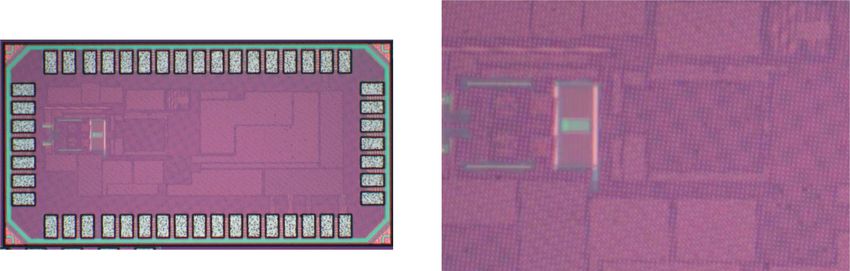
The VCO-based ADC was fabricated in a 65 nm TSMC devices was measured (Fig. 13). The average SFDR is 107.9 dB
LP process and occupied an active area of 0.075 mm2 . An and consistently above 104 dB. The SNDR as a function of
annotated die micrograph is shown in Fig. 11. The 1st integrator, frequency from 1 Hz to 1 kHz is shown in Fig. 14. The SNDR
impedance-booster, and CDAC are powered from a 1.2 V supply varies by less than 0.7 dB across the entire frequency range.
while the multi-phase TDC quantizer and the digital blocks The ADC input-referred noise was measured with shorted
containing the summer and DEM logic operate at 0.8 V. inputs. The PSD is shown in Fig. 15. The integrated noise from
Authorized licensed use limited to: Univ of Calif San Diego. Downloaded on February 19,2022 at 00:49:12 UTC from IEEE Xplore. Restrictions apply.POCHET et al.: 174.7-DB FOM, 2ND -ORDER VCO-BASED EXG-TO-DIGITAL FRONT-END USING 1291
Fig. 18. Measured common-mode rejection ratio (CMRR) with a 200 mVpp
(orange) and a 400 mVpp (blue) common-mode input.
Fig. 19. Square wave and sinusoid combined.
Fig. 21. ExG measurements: (a) ECG, (b) EOG, and (c) EMG.
artifacts/interference, the distortion would be below the noise
floor and thus not introduce any unwanted signals.
Fig. 20. Measured input impedance with and without boosting. The common-mode rejection ratio (CMRR) was measured
across the bandwidth with a full-scale ADC input (200 mVpp
single-ended) and was above 95 dB over the entire frequency
1 Hz to 1 kHz is 3.5 µVrms , and the spot noise is 110 nV/Hz. range. Since a larger common-mode artifact is expected in a
The 1/f noise in the spectrum is mainly due to the inverters in wearable device (up to 400 mVpp ), the ADC’s CMRR was
the 1st CCO, which are not chopped. However, this is less than measured with this larger input to be 82 dB. Common-mode
15% of the integrated noise. artifacts larger than 400 mVpp cause the ADC’s loop stability
Fig. 16 shows the measured 92.3 dB DR and the power as a to degrade, leading to a loss in performance. It should be noted
function of the amplitude. The pie charts show that the system that the results are better than reported in the original paper [25]
power reduced from 5.8 to 4.25 µW (35%) when the input due to an improvement in the testing setup. The insensitivity
amplitude was below 10 mV. As expected, the power of the to large and rapid artifacts was tested by superimposing a 150
GIRO and digital blocks reduce significantly, and the power µVpp sinusoid signal on a 300 mVpp square wave. As illustrated
consumption is dominated by the input Gm -cell. This results in Fig. 19, the ADC quickly recovers from the artifact, allowing
from the input-dependent quantizer duty-cycling, enabling low the small sinusoidal to be clearly observed.
power in the absence of motion artifacts. To measure the input impedance, Zin , high precision 1 MΩ
The ADC was excited with two tones at 200 mVpp to resistors were placed in series with the ADC inputs and the
evaluate the impact of large motion artifacts on the linearity. voltage across them amplified by an instrumentation amplifier.
Fig. 17 shows the measured intermodulation distortion (IMD) Fig. 20 shows Zin measured across the bandwidth with and
was 99.8 dBc with the intermodulation products ∼1 µV, which without activating the auxiliary path booster. Zin is boosted by
is below the 3.5 µVrms integrated noise of the AFE. This 12× when the auxiliary path is enabled and is >50 MΩ across
demonstrates that even in the presence of significant motion the entire bandwidth.
Authorized licensed use limited to: Univ of Calif San Diego. Downloaded on February 19,2022 at 00:49:12 UTC from IEEE Xplore. Restrictions apply.1292 IEEE TRANSACTIONS ON BIOMEDICAL CIRCUITS AND SYSTEMS, VOL. 15, NO. 6, DECEMBER 2021
TABLE I
PERFORMANCE SUMMARY AND COMPARISON TO THE STATE-OF-THE-ART
B. Biological Measurements integrating and time-encoding VCO-based 1st stage followed by
This ADC was validated by measuring various ExG signals a multi-phase, multi-quantizer noise-shaped TDC. The system’s
with 3M red dot electrodes on a healthy volunteer. Fig. 21(a) linearity is further improved using a GIRO that significantly
shows the waveform from a three-lead chest ECG recording. reduces the mismatch sensitivity. Leveraging the time-based
Around 8 seconds into the recording, motion artifacts were processing of the ADC, the system’s power is naturally duty-
purposely generated to showcase the ability of the system to cycled with the input amplitude leading to 35% power savings
correctly digitize the ECG waveform in the presence of large in the absence of artifacts. To achieve the high input impedance
motion artifacts like one would encounter with a wearable in a required to interface with small electrodes, an input-impedance
non-stationary environment. The system does not saturate, and boosting circuit is placed around the input-chopper boosting
the ECG waveform can be observed and extracted despite the the input impedance by 12× and guaranteeing >50 MΩ input
large motion artifact. The system was also used to measure EOG impedance over the entire bandwidth while achieving very high
[Fig. 21(b)] and EMG [Fig. 21(c)] showing that the system can linearity, low noise, and high power-efficiency.
measure standard ExG waveforms.
REFERENCES
C. Comparison to the State-of-the-Art
[1] X. Yang et al., “A 108 dB DR hybrid-CTDT direct-digitalization ΔΣ-
Table I compares this work with recently published direct ΣM front-end with 720 mVpp input range and >300 mV offset removal
digitization ADCs operating in the time and the voltage do- for wearable bio-signal recording,” in Proc. Symp. VLSI Circuits, 2019,
pp. C296–C297, doi: 10.23919/VLSIC.2019.8778185.
mains. This work achieves excellent linearity due to the im- [2] S. Mondal, C.-L. Hsu, R. Jafari, and D. Hall, “A dynamically recon-
proved matching of the proposed GIRO-based quantizer. The figurable ECG analog front-end with a 2.5 × data-dependent power
time-domain signal processing also enables significant power reduction,” in Proc. IEEE Custom Integr. Circuits Conf., 2017, pp. 1–4,
doi: 10.1109/CICC.2017.7993705.
savings in the “nominal” operating state (i.e., in the absence of [3] S. Mondal and D. A. Hall, “A 13.9-nA ECG amplifier achiev-
artifacts). This work achieves a competitive Schreier figure-of- ing 0.86/0.99 NEF/PEF using AC-coupled OTA-stacking,” IEEE
merit (FoM) of 174.7 dB while maintaining an input impedance J. Solid-State Circuits, vol. 55, no. 2, pp. 414–425, Feb. 2020,
doi: 10.1109/JSSC.2019.2957193.
>50 MΩ over the entire bandwidth of interest. [4] Y. Zheng et al., “Unobtrusive sensing and wearable devices for health
informatics,” IEEE Trans. Biomed. Eng., vol. 61, no. 5, pp. 1538–1554,
May 2014, doi: 10.1109/TBME.2014.2309951.
VI. CONCLUSION [5] J. Andreu-Perez, D. R. Leff, H. M. D. Ip, and G. Yang, “From wearable
sensors to smart implants—toward pervasive and personalized healthcare,”
This paper presents a direct-digitization VCO-based ADC IEEE Trans. Biomed. Eng., vol. 62, no. 12, pp. 2750–2762, Dec. 2015,
for biopotential recording that achieves over 90 dB SNDR and doi: 10.1109/TBME.2015.2422751.
[6] J. Warchall, P. Theilmann, Y. Ouyang, H. Garudadri, and P. P. Mercier,
100 dB SFDR enabling it to digitize small ExG signals in “Robust biopotential acquisition via a distributed multi-channel FM-
the presence of large motion artifacts and interference. This is ADC,” IEEE Trans. Biomed. Circuits Syst., vol. 13, no. 6, pp. 1229–1242,
accomplished by enabling second-order noise-shaping using an Dec. 2019, doi: 10.1109/TBCAS.2019.2941846.
Authorized licensed use limited to: Univ of Calif San Diego. Downloaded on February 19,2022 at 00:49:12 UTC from IEEE Xplore. Restrictions apply.POCHET et al.: 174.7-DB FOM, 2ND -ORDER VCO-BASED EXG-TO-DIGITAL FRONT-END USING 1293
[7] S. Lee, L. Yan, T. Roh, S. Hong, and H. Yoo, “A 75 µ w real-time scalable [26] G. Taylor and I. Galton, “A reconfigurable mostly-digital delta-sigma ADC
body area network controller and a 25 µW ExG sensor IC for compact with a worst-case FOM of 160 dB,” IEEE J. Solid-State Circuits, vol. 48,
sleep monitoring applications,” IEEE J. Solid-State Circuits, vol. 47, no. 1, no. 4, pp. 983–995, Apr. 2013, doi: 10.1109/JSSC.2013.2239113.
pp. 323–334, Jan. 2012, doi: 10.1109/JSSC.2011.2170636. [27] Y. Zhong et al., “A second-order purely VCO-based CT ΔΣ ADC using a
[8] A. Searle and L. Kirkup, “A direct comparison of wet, dry and insu- modified DPLL structure in 40-nm CMOS,” IEEE J. Solid-State Circuits,
lating bioelectric recording electrodes,” Physiol. Meas., vol. 21, no. 2, vol. 55, no. 2, pp. 356–368, Feb. 2020, doi: 10.1109/JSSC.2019.2948008.
pp. 271–283, May 2000, doi: 10.1088/0967-3334/21/2/307. [28] V. Dhanasekaran et al., “A continuous time multi-bit ΔΣ ADC using time
[9] G. Li, S. Wang, and Y. Y. Duan, “Towards gel-free electrodes: A systematic domain quantizer and feedback element,” IEEE J. Solid-State Circuits,
study of electrode-skin impedance,” Sensors Actuators B: Chem., vol. 241, vol. 46, no. 3, pp. 639–650, Mar. 2011, doi: 10.1109/JSSC.2010.2099893.
pp. 1244–1255, Mar. 2017, doi: 10.1016/j.snb.2016.10.005. [29] K. Reddy, S. Dey, S. Rao, B. Young, P. Prabha, and P. K. Hanumolu, “A
[10] H. Chandrakumar and D. Markovic, “An 80-mVpp linear-input range, 54mW 1.2GS/s 71.5dB SNDR 50MHz BW VCO-based CT ΔΣ ADC
1.6-GΩ input impedance, low-power chopper amplifier for closed-loop using dual phase/frequency feedback in 65nm CMOS,” in Proc. Symp.
neural recording that is tolerant to 650-mVpp common-mode interfer- VLSI Circuits, 2015, pp. C256–C257, doi: 10.1109/VLSIC.2015.7231278.
ence,” in Proc. IEEE Int. Solid-State Circuits Conf., 2017, pp. 1–18, [30] K. Reddy et al., “A 16-mW 78-dB SNDR 10-MHz BW ctδσ
doi: 10.1109/JSSC.2017.2753824. ADC using residue-cancelling VCO-based quantizer,” IEEE J.
[11] D. Seok, S. Lee, M. Kim, J. Cho, and C. Kim, “Motion artifact removal Solid-State Circuits, vol. 47, no. 12, pp. 2916–2927, Dec. 2012,
techniques for wearable EEG and PPG sensor systems,” Front. Electron., doi: 10.1109/JSSC.2012.2218062.
vol. 2, 2021, Art. no. 4, doi: 10.3389/felec.2021.685513. [31] E. Gutierrez, P. Rombouts, and L. Hernandez, “Why and how VCO-
[12] X. Jiang, G.-B. Bian, and Z. Tian, “Removal of artifacts from EEG based ADCs can improve instrumentation applications,” in Proc.
signals: A review,” Sensors, vol. 19, no. 5, Feb. 2019, Art. no. 987, 25th IEEE Int. Conf. Electron., Circuits Syst., 2018, pp. 101–104,
doi: 10.3390/s19050987. doi: 10.1109/ICECS.2018.8618004.
[13] H. Kassiri et al., “Rail-to-rail-input dual-radio 64-channel closed-loop neu- [32] C. Tu, Y. Wang, and T. Lin, “A 0.06mm2± 50mV range −82dB THD chop-
rostimulator,” IEEE J. Solid-State Circuits, vol. 52, no. 11, pp. 2793–2810, per VCO-based sensor readout circuit in 40nm CMOS,” in Proc. Symp.
Nov. 2017, doi: 10.1109/JSSC.2017.2749426. VLSI Circuits, 2017, pp. C84–C85, doi: 10.23919/VLSIC.2017.8008558.
[14] C. Kim, S. Joshi, H. Courellis, J. Wang, C. Miller, and G. Cauwenberghs, [33] Y. Zhong et al., “A second-order purely VCO-based CT ΔΣ ADC using a
“Sub- µ Vrms-noise sub- µ W/Channel ADC-direct neural recording with modified DPLL structure in 40-nm CMOS,” IEEE J. Solid-State Circuits,
200-mV/ms transient recovery through predictive digital autoranging,” vol. 55, no. 2, pp. 356–368, Feb. 2020, doi: 10.1109/JSSC.2019.2948008.
IEEE J. Solid-State Circuits, vol. 53, no. 11, pp. 3101–3110, Nov. 2018, [34] “Understanding delta-sigma data converters | IEEE eBooks | IEEE xplore.”
doi: 10.1109/JSSC.2018.2870555. Accessed: Jul. 31, 2021. [Online]. Available: https://ieeexplore.ieee.org/
[15] W. Jiang, V. Hokhikyan, H. Chandrakumar, V. Karkare, and book/5264508
D. Markovic, “A ±50-mV linear-input-range VCO-based neural- [35] A. Jayaraj, M. Danesh, S. T. Chandrasekaran, and A. Sanyal,
recording front-end with digital nonlinearity correction,” IEEE J. “Highly digital second-order $\Delta\Sigma$ VCO ADC,” IEEE
Solid-State Circuits, vol. 52, no. 1, pp. 173–184, Jan. 2017, Trans. Circuits Syst. I, vol. 66, no. 7, pp. 2415–2425, Jul. 2019,
doi: 10.1109/JSSC.2016.2624989. doi: 10.1109/TCSI.2019.2898415.
[16] S. Li et al., “A 0.025-mm2 0.8-V 78.5dB-SNDR VCO-based [36] A. Jayaraj, M. Danesh, S. T. Chandrasekaran, and A. Sanyal, “76-dB DR,
sensor readout circuit in a hybrid PLL-ΔΣM structure,” in 48 fJ/Step second-order VCO-Based Current-to-Digital converter,” IEEE
Proc. IEEE Custom Integr. Circuits Conf., 2019, pp. 1–3, Trans. Circuits Syst. I: Regular Papers, vol. 67, no. 4, pp. 1149–1157,
doi: 10.1109/CICC.2019.8780175. Apr. 2020, doi: 10.1109/TCSI.2019.2941956.
[17] M. R. Pazhouhandeh, M. Chang, T. A. Valiante, and R. Genov, “Track-and- [37] A. Elshazly, S. Rao, B. Young, and P. K. Hanumolu, “A noise-shaping
Zoom neural Analog-to-Digital converter with blind stimulation artifact Time-to-Digital converter using switched-ring oscillators—Analysis, de-
rejection,” IEEE J. Solid-State Circuits, vol. 55, no. 7, pp. 1984–1997, sign, and measurement techniques,” IEEE J. Solid-State Circuits, vol. 49,
Jul. 2020, doi: 10.1109/JSSC.2020.2991526. no. 5, pp. 1184–1197, May 2014, doi: 10.1109/JSSC.2014.2305651.
[18] J. Huang and P. P. Mercier, “A 112-dB SFDR 89-dB SNDR VCO-based [38] B. Drost, M. Talegaonkar, and P. K. Hanumolu, “Analog filter design using
sensor front-end enabled by background-calibrated differential pulse code ring oscillator integrators,” IEEE J. Solid-State Circuits, vol. 47, no. 12,
modulation,” IEEE J. Solid-State Circuits, vol. 56, no. 4, pp. 1046–1057, pp. 3120–3129, Dec. 2012, doi: 10.1109/JSSC.2012.2225738.
Apr. 2021, doi: 10.1109/JSSC.2020.3037833. [39] M. Z. Straayer and M. H. Perrott, “A multi-path gated ring oscillator TDC
[19] J. Huang and P. P. Mercier, “28.1 A distortion-free VCO-based with first-order noise shaping,” IEEE J. Solid-State Circuits, vol. 44, no. 4,
Sensor-to-Digital front-end achieving 178.9dB FoM and 128dB SFDR pp. 1089–1098, Apr. 2009, doi: 10.1109/JSSC.2009.2014709.
with a calibration-free differential pulse-code modulation technique,” [40] X. Yi, Z. Liang, C. C. Boon, G. Feng, F. Meng, and K. Yang, “An
in Proc. IEEE Int. Solid- State Circuits Conf., 2021, pp. 386–388, inverted ring oscillator noise-shaping Time-to-Digital converter with in-
doi: 10.1109/ISSCC42613.2021.9365950. band noise reduction and coherent noise cancellation,” IEEE Trans. Cir-
[20] H. Jeon, J. Bang, Y. Jung, I. Choi, and M. Je, “A high DR, DC-Coupled, cuits Syst. I: Regular Papers, vol. 67, no. 2, pp. 686–698, Feb. 2020,
time-based neural-recording IC with degeneration R-DAC for bidirec- doi: 10.1109/TCSI.2019.2949732.
tional neural interface,” IEEE J. Solid-State Circuits, vol. 54, no. 10, [41] C.-W. Yao et al., “A 14-nm 0.14-psrms Fractional-N digital PLL with
pp. 2658–2670, Oct. 2019, doi: 10.1109/JSSC.2019.2930903. a 0.2-ps resolution ADC-Assisted coarse/fine-conversion chopping TDC
[21] H. Chandrakumar and D. Marković, “A 15.2-ENOB 5-kHz BW 4.5- µ W and TDC nonlinearity calibration,” IEEE J. Solid-State Circuits, vol. 52,
chopped CT ΔΣ -ADC for artifact-tolerant neural recording front ends,” no. 12, pp. 3446–3457, Dec. 2017, doi: 10.1109/JSSC.2017.2742518.
IEEE J. Solid-State Circuits, vol. 53, no. 12, pp. 3470–3483, Dec. 2018, [42] S. T. Chandrasekaran and A. Sanyal, “Stochastic ΔΣ VCO-ADC utilizing
doi: 10.1109/JSSC.2018.2876468. 4× staggered averaging,” in Proc. IEEE Int. Symp. Circuits Syst., 2020,
[22] J.-S. Bang, H. Jeon, M. Je, and G.-H. Cho, “A 6.5µW 92.3dB-DR pp. 1–5, doi: 10.1109/ISCAS45731.2020.9180835.
biopotential-recording front-end with 360mVpp linear input range,” in [43] M. J. M. Pelgrom, A. C. J. Duinmaijer, and A. P. G. Welbers, “Matching
Proc. Symp. VLSI Circuits Dig. Tech. Papers, 2018, Art. no. 2. properties of MOS transistors,” IEEE J. Solid-State Circuits, vol. 24, no. 5,
[23] P. R. Kinget, “Scaling analog circuits into deep nanoscale CMOS: Obsta- pp. 1433–1439, Oct. 1989, doi: 10.1109/JSSC.1989.572629.
cles and ways to overcome them,” in Proc. IEEE Custom Integr. Circuits [44] A. Sheikholeslami, “Process variation and pelgrom’s law [Circuit intu-
Conf., 2015, pp. 1–8, doi: 10.1109/CICC.2015.7338394. itions],” IEEE Solid-State Circuits Mag., vol. 7, no. 1, pp. 8–9, Win-
[24] C. Lee et al., “A 6.5-µW 10-kHz BW 80.4-dB SNDR Gm -C-based CT ter 2015, doi: 10.1109/MSSC.2014.2369331.
ΔΣ modulator with a feedback-assisted Gm linearization for artifact- [45] H. Omran, H. Alahmadi, and K. N. Salama, “Matching properties of
tolerant neural recording,” IEEE J. Solid-State Circuits, vol. 55, no. 11, femtofarad and sub-femtofarad MOM capacitors,” IEEE Trans. Cir-
pp. 2889–2901, Nov. 2020, doi: 10.1109/JSSC.2020.3018478. cuits Syst. I: Regular Papers, vol. 63, no. 6, pp. 763–772, Jun. 2016,
[25] C. Pochet, J. Huang, P. P. Mercier, and D. A. Hall, “28.4 A doi: 10.1109/TCSI.2016.2537824.
400mVpp 92.3 dB-SNDR 1kHz-BW 2nd-Order VCO-based exg-to- [46] A. C. Sun, E. Alvarez-Fontecilla, A. G. Venkatesh, E. Aronoff-Spencer,
Digital front-end using a multiphase gated-inverted ring-oscillator quan- and D. A. Hall, “High-Density redox amplified coulostatic discharge-
tizer,” in Proc. IEEE Int. Solid- State Circuits Conf., 2021, pp. 392–394, based biosensor array,” IEEE J. Solid-State Circuits, vol. 53, no. 7,
doi: 10.1109/ISSCC42613.2021.9365985. pp. 2054–2064, Jul. 2018, doi: 10.1109/JSSC.2018.2820705.
Authorized licensed use limited to: Univ of Calif San Diego. Downloaded on February 19,2022 at 00:49:12 UTC from IEEE Xplore. Restrictions apply.1294 IEEE TRANSACTIONS ON BIOMEDICAL CIRCUITS AND SYSTEMS, VOL. 15, NO. 6, DECEMBER 2021
Corentin Pochet (Student Member, IEEE) received Drew A. Hall (Senior Member, IEEE) received the
the B.S. and M.E. degrees in electrical engineering B.S. degree in computer engineering (with Hons.)
from the joint program between the Université Libre from the University of Nevada, Las Vegas, NV, USA,
de Bruxelles and the Vrije Universiteit Brussel, Brus- in 2005, and the M.S. and Ph.D. degrees in electrical
sels, Belgium, in 2014 and 2016, respectively. He is engineering from Stanford University, Stanford, CA,
currently working toward the Ph.D. degree in electri- USA, in 2008 and 2012, respectively.
cal and computer engineering with the University of From 2011 to 2013, he was a Research Scientist
California at San Diego, La Jolla, CA,USA. His re- with the Integrated Biosensors Laboratory, Intel Cor-
search interests include designing low-power analog poration, Santa Clara, CA. Since 2013, he has been
front-end circuits and time-based analog-to-digital with the Department of Electrical and Computer En-
converters for wearable and biomedical applications. gineering, University of California, San Diego, CA,
Mr. Pochet was the recipient of the Belgian American Education Foundation where he is currently an Associate Professor. His research interests include
(B.A.E.F) Henri Benedictus Fellowship in 2016. bioelectronics, biosensors, analog circuit design, medical electronics, and sensor
interfaces.
Dr. Hall won First Place in the Inaugural International IEEE Change the World
Competition and First Place in the BME-IDEA invention competition, both in
Jiannan Huang (Member, IEEE) received the B.S.
2009. He was the recipient of the Analog Devices Outstanding Designer Award
degree in electrical engineering from the University in 2011, Undergraduate Teaching Award in 2014, Hellman Fellowship Award
of Michigan, Ann Arbor, MI, USA, with outstand-
in 2014, NSF CAREER Award in 2015, and NIH Trailblazer Award in 2019.
ing achievement, and Shanghai Jiao Tong University,
He is also a Tau Beta Pi Fellow. He has been an Associate Editor for IEEE
Shanghai, China, in 2016, and the M.S. and Ph.D.
TRANSACTIONS ON BIOMEDICAL INTEGRATED CIRCUITS since 2015, a Member
degrees in electrical and computer engineering from
of the CICC Technical Program Committee since 2017, a Member of the ISSCC
the University of California, San Diego, La Jolla, CA,
Technical Program Committee since 2020, and an Associate Editor for IEEE
USA, in 2018 and 2021, respectively.
SOLID-STATE CIRCUITS LETTERS since 2021.
He has held internship positions with Analog De-
vices, Wilmington, MA, USA, MaXentric Technolo-
gies, La Jolla, and Movellus Circuits, Ann Arbor, MI,
where he worked on high-performance, low-power mixed-signal circuits. In
2021, he joined Qualcomm Inc., San Diego, as an Analog or mixed-signal De-
sign Engineer. His research interests include analog or mixed-signal integrated
circuits with a particular focus on developing high-resolution VCO-based ADCs
using digital calibrations.
Patrick P. Mercier (Senior Member, IEEE) received
the B.Sc. degree in electrical and computer engineer-
ing from the University of Alberta, Edmonton, AB,
Canada, in 2006, and the S.M. and Ph.D. degrees in
electrical engineering and computer science from the
Massachusetts Institute of Technology (MIT), Cam-
bridge, MA, USA, in 2008 and 2012, respectively.
He is currently an Associate Professor in electri-
cal and computer engineering with the University of
California, San Diego, CA, USA, where he is also the
Co-Director of the Center for Wearable Sensors and
the Site Director of the Power Management Integration Center. His research
interests include the design of energy-efficient microsystems, focusing on the
design of RF circuits, power converters, and sensor interfaces for miniaturized
systems and biomedical applications.
Prof. Mercier was the recipient of the Natural Sciences and Engineering
Council of Canada (NSERC) Julie Payette Fellowship in 2006, NSERC Post-
graduate Scholarships in 2007 and 2009, Intel Ph.D. Fellowship in 2009, 2009
IEEE International Solid-State Circuits Conference (ISSCC) Jack Kilby Award
for Outstanding Student Paper at ISSCC 2010, Graduate Teaching Award in
Electrical and Computer Engineering with UCSD in 2013, Hellman Fellowship
Award in 2014, Beckman Young Investigator Award in 2015, DARPA Young
Faculty Award in 2015, UC San Diego Academic Senate Distinguished Teaching
Award in 2016, Biocom Catalyst Award in 2017, NSF CAREER Award in 2018,
National Academy of Engineering Frontiers of Engineering Lecture in 2019,
and San Diego County Engineering Council Outstanding Engineer Award in
2020. From 2015 to 2017, he was an Associate Editor for IEEE TRANSACTIONS
ON VERY LARGE SCALE INTEGRATION (TVLSI). Since 2013, he has been an
Associated Editor for IEEE TRANSACTIONS ON BIOMEDICAL CIRCUITS AND
SYSTEMS (TBioCAS), and is currently a Member of the ISSCC International
Technical Program Committee, the CICC Technical Program Committee, the
VLSI Symposium Technical Program Committee, and an Associate Editor for
IEEE SOLID-STATE CIRCUITS LETTERS. Prof. Mercier was the Co-Editor of the
Ultra-Low-Power Short-Range Radios (Springer, 2015), Power Management
Integrated Circuits (CRC Press, 2016), and High-Density Electrocortical Neural
Interfaces (Academic Press, 2019).
Authorized licensed use limited to: Univ of Calif San Diego. Downloaded on February 19,2022 at 00:49:12 UTC from IEEE Xplore. Restrictions apply.You can also read